Make: More Electronics (2014)
Chapter 15. Experiment 15: It's All So Logical!
In Make: Electronics I provided an introduction to digital logic, but I avoided the more challenging aspects, and I didn’t deal with components such as multiplexers or shift registers. Logic chips of this kind are less widely used today than they used to be, but logic itself remains fundamental to all computing devices. So let’s go deeper, now, into that world, to learn how it works—and have some fun.
Experiment 15: Telepathy Test
This first logic project seems ridiculously simple. All you need are four pushbuttons, a couple of chips, and an LED. As we delve deeper, though, you’ll find that it’s not quite so simple after all.
The ostensible purpose of this experiment is to test your capability for extrasensory perception, which is often known by its acronym, ESP. I’ll call the circuit a Telepathy Tester.
Background: ESP
For many decades, researchers at the fringes of conventional science have looked for evidence of paranormal abilities in the human brain. J. B. Rhine was one of the pioneers, working at Duke University. His book Extrasensory Perception was published in 1934, and he continued to report serious research through the 1970s. A big criticism of his record has been that on several occasions, he discovered that his research assistants were cheating. This may have been because they actually believed in ESP and didn’t want one unsuccessful day to bring down their average score. Bear this in mind, if you try this project: even people who have good intentions may try to fool you, if they are also fooling themselves.
The Setup
True “mind reading” doesn’t happen often (if at all), and therefore we have to adopt a statistical approach, making dozens or even thousands of attempts, and comparing the success rate with the outcome that we would expect from chance alone.
The experiment that I’ll describe is intended to be used on that basis. Two buttons are placed in front of one person, and two more buttons are placed in front of a second person, seated opposite. A screen prevents either person from seeing the other’s hands.Figure 15-1 gives you an idea of what I have in mind, viewed from above. You may not feel inclined to build the whole thing, especially if you don’t have a suitable collaborator. But you can improvise, and you should assemble the components of the circuit to see how it works.
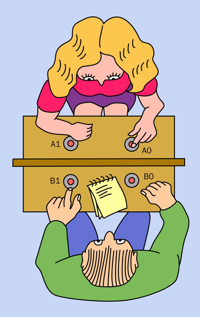
Figure 15-1. Viewed from above, Annabel and Boris get ready to test their capabilities in extrasensory perception.
I’m going to name the participants Annabel and Boris, because I like distinctive names that are easy to remember. I’ll abbreviate them as A and B in some of the diagrams.
You’ll notice that the buttons in front of Annabel are identified as A0 and A1, while the buttons in front of Boris are B0 and B1. The goal is for them to press buttons directly opposite each other, by trying to sense each others’ intentions telepathically. If Annabel presses A0 and Boris presses B0, or if they press A1 and B1, those are successes. Conversely, A0 and B1, or A1 and B0, are failures.
Because there are four possible combinations, and only two of them indicate a success, the odds are 50-50. A significant deviation from this result could be an indication of one person sensing the other person’s intentions with psychic powers—or could indicate that someone is cheating. I’ll deal with the problem of cheat detection a bit later.
Figure 15-2 shows how AND and OR logic gates can be used with the pushbuttons to confirm that a trial has been successful.
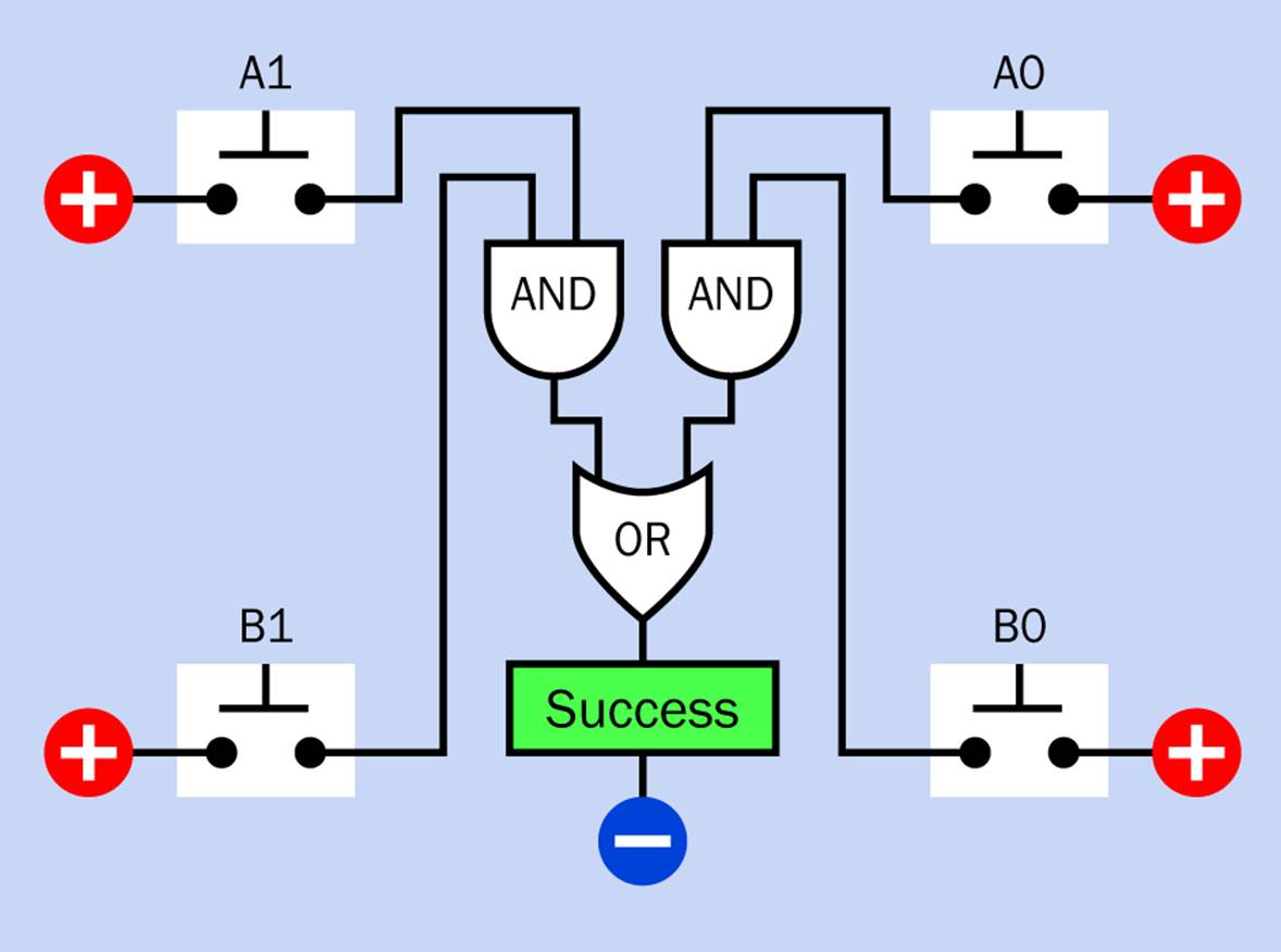
Figure 15-2. These logic gates will activate a “success” indicator if A0 and B0 are both pressed, or if A1 and B1 are both pressed.
If you don’t remember the symbols and functions associated with logic gates, the six primary variants are shown in Figure 15-3 and Figure 15-4, with high and low inputs and outputs indicated by red and black, respectively.
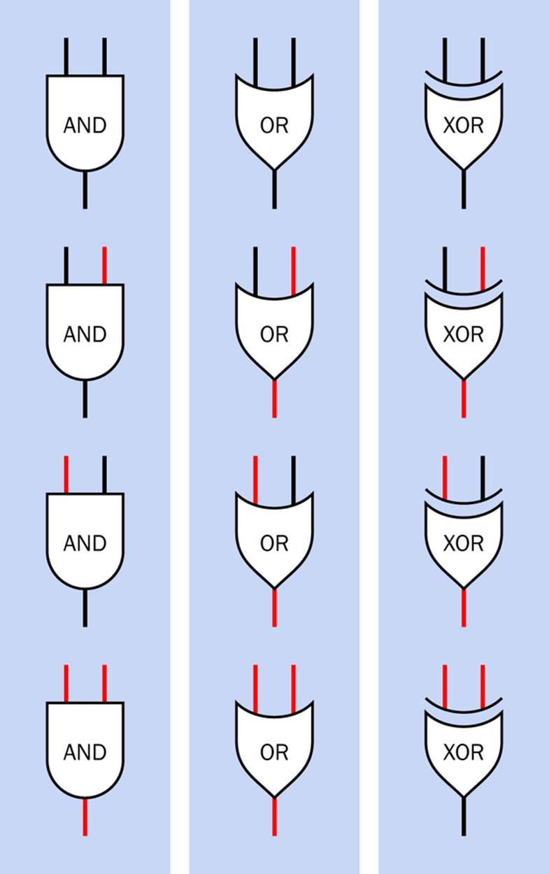
Figure 15-3. Inputs are often shown above each logic gate, while the output of each gate is below it. If each of the two inputs can have a high or low state (represented by red or black in this figure), there are four possible combinations, each of which produces an output defined here.
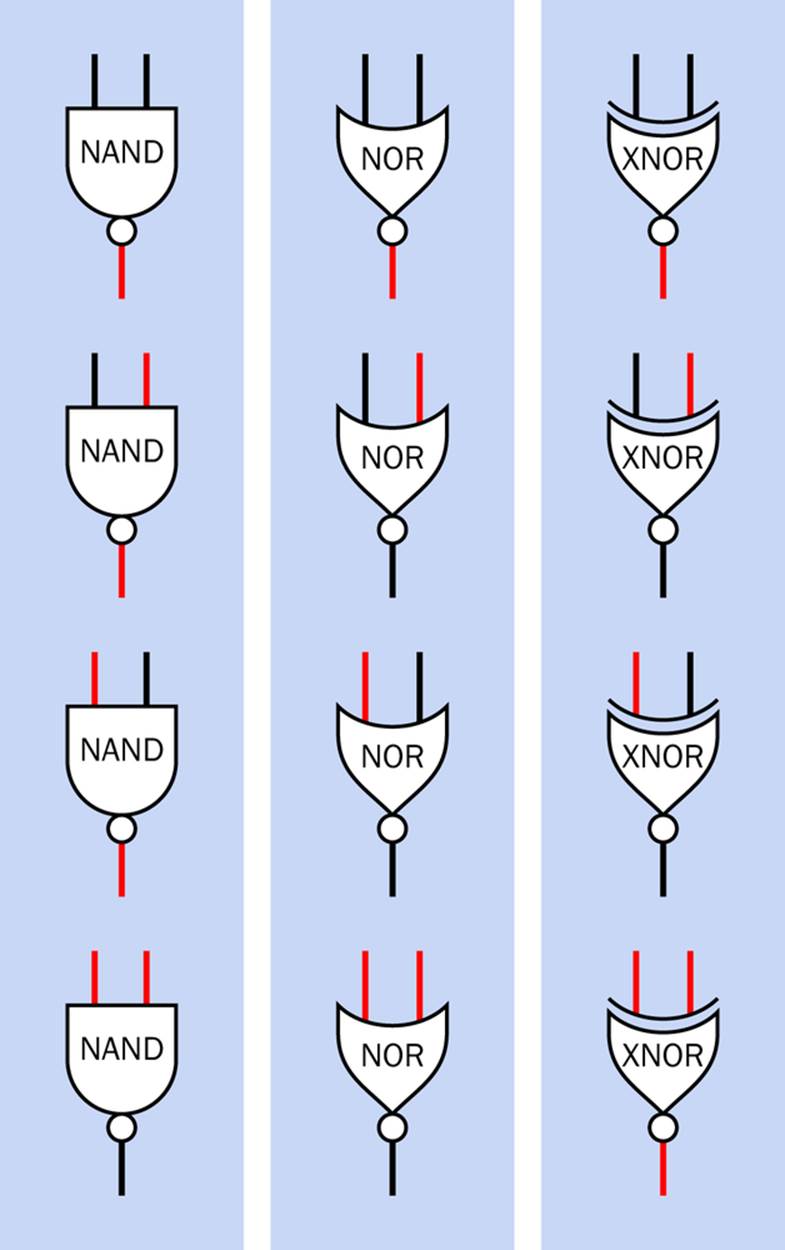
Figure 15-4. Inputs and outputs for NAND, NOR, and XNOR gates. A red line indicates a high input or output, while a black line indicates a low input or output.
For quick reference, Figure 15-5 shows the four possible input combinations in the column on the left, and the corresponding outputs for each gate, beside it.
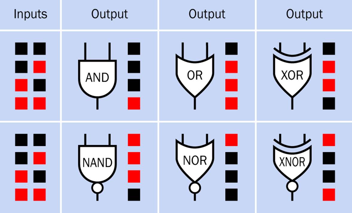
Figure 15-5. This quick-reference chart shows the four possible input combinations and the resulting output that each gate will generate.
Any time I use logic symbols in the development of a circuit, you can use simulation software to test the logic and demonstrate its behavior. For instance, http://www.neuroproductions.be/logic-lab/ is a free online simulator. You may have to turn my logic diagrams around before creating them on the simulator, because I tend to show a logic flow running from top to bottom, while the simulator is more inclined to show it from left to right. In any case, a logic simulator is just an intermediate step before you build a circuit in hardware.
Quick Facts About Logic Chips
§ Each logic gate is composed of multiple transistors etched into silicon. The original through-hole DIP packages for logic gates had 14 pins and are still being made today, although surface-mount versions have become widely used.
§ Although computers are not built from logic chips anymore, gates still find some uses—as in “glue logic,” which links different sections of a circuit board.
§ A 14-pin chip may contain four two-input gates, three three-input gates, two four-input gates, or one eight-input gate. These configurations are known as quad, triple, dual, and single, describing how many gates are inside the chip.
§ All the gates inside a multigate chip function completely independently of each other.
§ The inputs of an unused gate in a chip should be grounded to prevent them from picking up and responding to electromagnetic fields.
§ A “high” input or output is close to the positive power supply, while a “low” input or output is close to 0VDC. Negative-logic chips also exist but are unusual.
§ Logic “families” are successive generations of chips that have been developed. I will be using the 74HC00 family, so called because all part numbers begin with the digits 74, while HC tells you that this is a high-speed CMOS chip. Two, three, or four digits can be used instead of 00 to identify each type of chip. Where necessary, I will also use some older CMOS chips in the 4000B family.
§ Be careful when ordering chips, because the part numbers for through-hole and surface-mount variants can be almost identical. Most online vendors provide a filter that will restrict a search to DIP or PDIP through-hole dual inline packages.
§ Logic chips are designed to be chained together so that the output of one connects directly to the input of the next, so long as they are both in the same family.
§ A logic chip is said to “source” current in its high-output state, and “sink” current in its low-output state.
§ Each logic chip in the HC family can source or sink up to 25mA of DC current, which is ample to power a generic LED. However, when you draw as much current as this from a chip, you pull down its output voltage. Use a meter to check the voltage when you are driving an LED, and be cautious of using that output also for an input to another logic chip. Increase the value of a series resistor with the LED if necessary.
§ Where a pushbutton or SPST switch is connected with the input of a logic gate, you must not allow the voltage on the input pin to “float” when the switch is open. Use a pulldown or pullup resistor to maintain a high or low voltage on the input pin. See Figure 15-6.
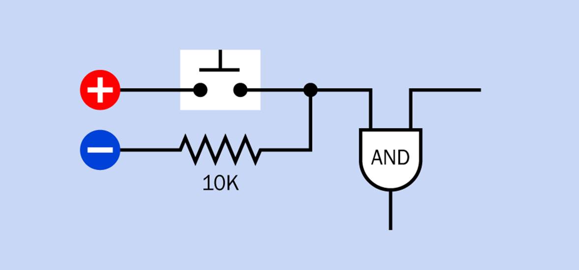
Figure 15-6. When positive power is being connected with the input of a logic gate via a pushbutton or electromechanical switch, a pulldown resistor must be used to keep the input from “floating” when the connection is open. If the positive and negative symbols are swapped, the resistor becomes a pullup resistor.
§ A logic diagram is not the same as a component schematic. In a logic diagram, such as the one shown in Figure 15-2, power supplies to logic gates are not usually shown, and pullup or pulldown resistors are also omitted. In a component schematic, chips with pin connections are shown instead of logic gates, and all necessary power connections are included.
ESP Logic
The concept of Figure 15-2 is very simple. It can be summarized in this sentence:
If buttons A0 AND B0 are pressed, OR if buttons A1 AND B1 are pressed, the outcome is a success.
There’s a clear comparison between the words AND and OR in that sentence, and the gates in the logic diagram.
I’m going to refer to the green rectangle in the diagram as an “indicator,” but it could be simply an LED that lights up to tell Annabel and Boris that they guessed correctly (or read each others’ minds, if you prefer to believe that this is what’s happening).
So far, the logic is elementary, but please just take a moment to build the circuit. As always, the hands-on process is the best way to learn.
Building It
The inner workings of the quad two-input AND and OR chips are shown in Figure 15-7.
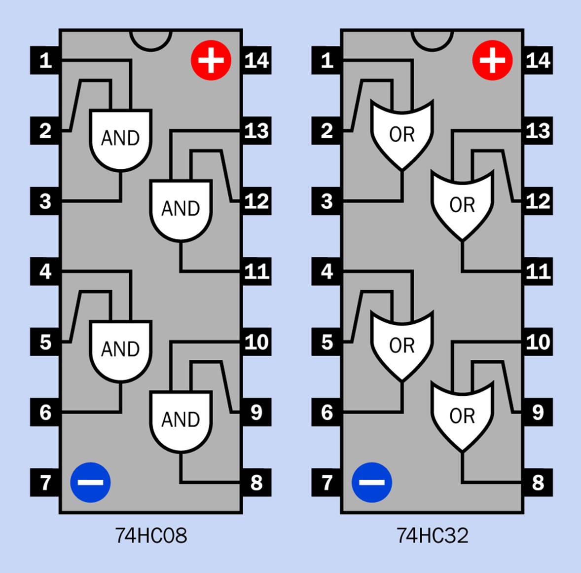
Figure 15-7. Each 14-pin logic chip can contain four separate two-input AND or OR logic gates, as shown here. These types of chips are referred to as quad two-input.
The schematic that corresponds with the logic diagram in Figure 15-2 is shown in Figure 15-8. I have squeezed some miniature representations of the gates into the chips to show what’s going on. “&” denotes an AND gate, while “O” is an OR gate. (These are not standardized abbreviations.)
§ The positive bus is now on the right-hand side of the schematic, as this is convenient to power the logic chips, which receive positive voltage on pin 14 in each case. Most of the circuits in the remainder of the book will have the positive bus on the right. Be careful not to power your chips with reversed polarity; they may never recover from the shock.
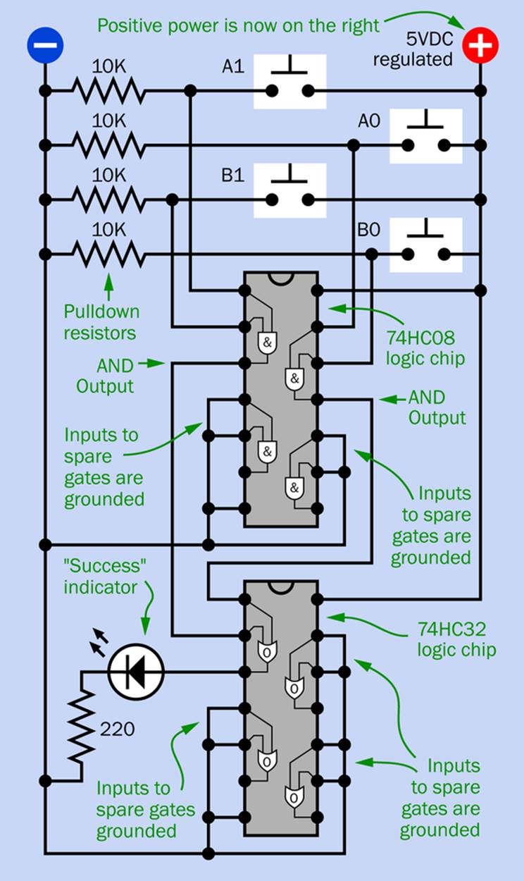
Figure 15-8. This schematic shows the simplest breadboardable version of the ESP test.
The breadboarded version of this circuit is shown in Figure 15-9.
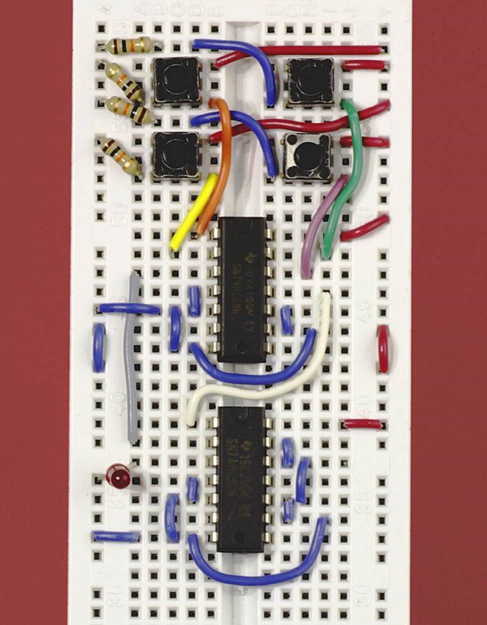
Figure 15-9. The simplest and most basic demonstration version of the Telepathy Tester. Pushbuttons for the participants are included as four tactile switches at the top. The LED at lower left is the only output.
I have not shown the 7805 voltage regulator and the two capacitors, which are always required with 74HC00 chips. Any time you see “5VDC regulated” on a schematic, you know that the voltage regulator and its capacitors are necessary.
Unused chip inputs must be tied to negative ground to prevent them from responding to stray electromagnetic fields. Unused outputs from each gate can be left unconnected.
You should find that if you press the pair of buttons labelled A0 and B0, or the buttons labelled A1 and B1, the LED lights up, while the other combinations of buttons will not do anything.
So far, so good. But now that you have the circuit in front of you, I think I can convince you that it badly needs some enhancements if it’s going to become seriously usable.
Making It Better
Generally, I thinking that we need to add user-friendly notifications and cheat-proofing:
§ In an ESP test, Annabel must not be able to see which button Boris is pressing, and Boris must not be able to see which button Annabel is pressing. This creates a problem: how does either person know when the next match will begin? Really we need a “ready” prompt for Annabel, which will light up when Boris is pressing a button but she hasn’t pressed hers yet; and a “ready” prompt for Boris, which will light up when Annabel is pressing a button but he hasn’t pressed his yet.
§ As I mentioned earlier, even sincere people may be tempted to cheat if they believe that their ESP powers need a little bit of help because they aren’t working well on this particular day. Unfortunately, in our Telepathy Test, cheating is really easy. A or B can guarantee a hit just by pressing both buttons at once!
§ Currently we only have one indicator that lights up when Annabel and Boris are successful. We should really have another indicator which lights up if they fail.
In the next experiment, I’ll implement these improvements—with some surprising results.
All materials on the site are licensed Creative Commons Attribution-Sharealike 3.0 Unported CC BY-SA 3.0 & GNU Free Documentation License (GFDL)
If you are the copyright holder of any material contained on our site and intend to remove it, please contact our site administrator for approval.
© 2016-2026 All site design rights belong to S.Y.A.