Make: More Electronics (2014)
Chapter 16. Experiment 16: Enhanced ESP
Before providing you with a revised schematic, I’m going to start by spelling out the requirements in words. I think a verbal description should always be the first step in developing a logic diagram.
The second step is to convert the logic diagram into a schematic that uses actual components.
Are You Ready?
Adding “ready” prompts to the Telepathy Tester seems easy enough. Perhaps I can express the task like this:
“If button A0 OR A1 is pressed, then an indicator tells Boris that Annabel is ready. Alternatively, if button B0 OR B1 is pressed, then another indicator shows Annabel that Boris is ready.”
Figure 16-1 translates these two sentences into a logic diagram. For the sake of clarity, I have shown this separately from the previous logic diagram in Figure 15-2. However, the two diagrams could be combined, as shown in Figure 16-2, because you can take the output from a single pushbutton and share it among two or more logic inputs. (In Figure 16-2 I have showed the connections from Figure 15-2 in gray, to distinguish them from the new connections.)
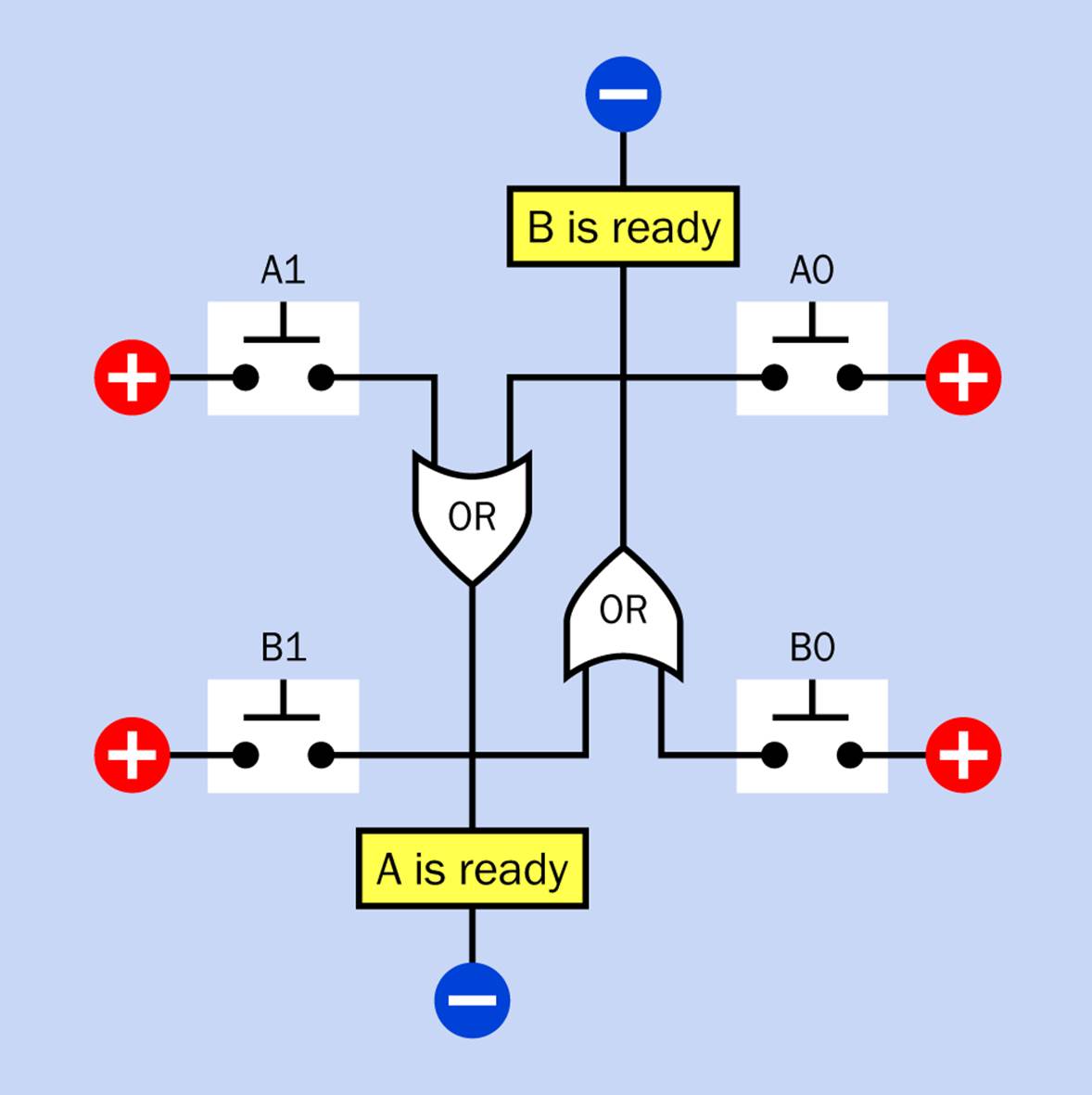
Figure 16-1. Two OR gates can be used to show each person if the other person has already pressed a button. The “ready” indicators do not reveal which button has actually been pressed.
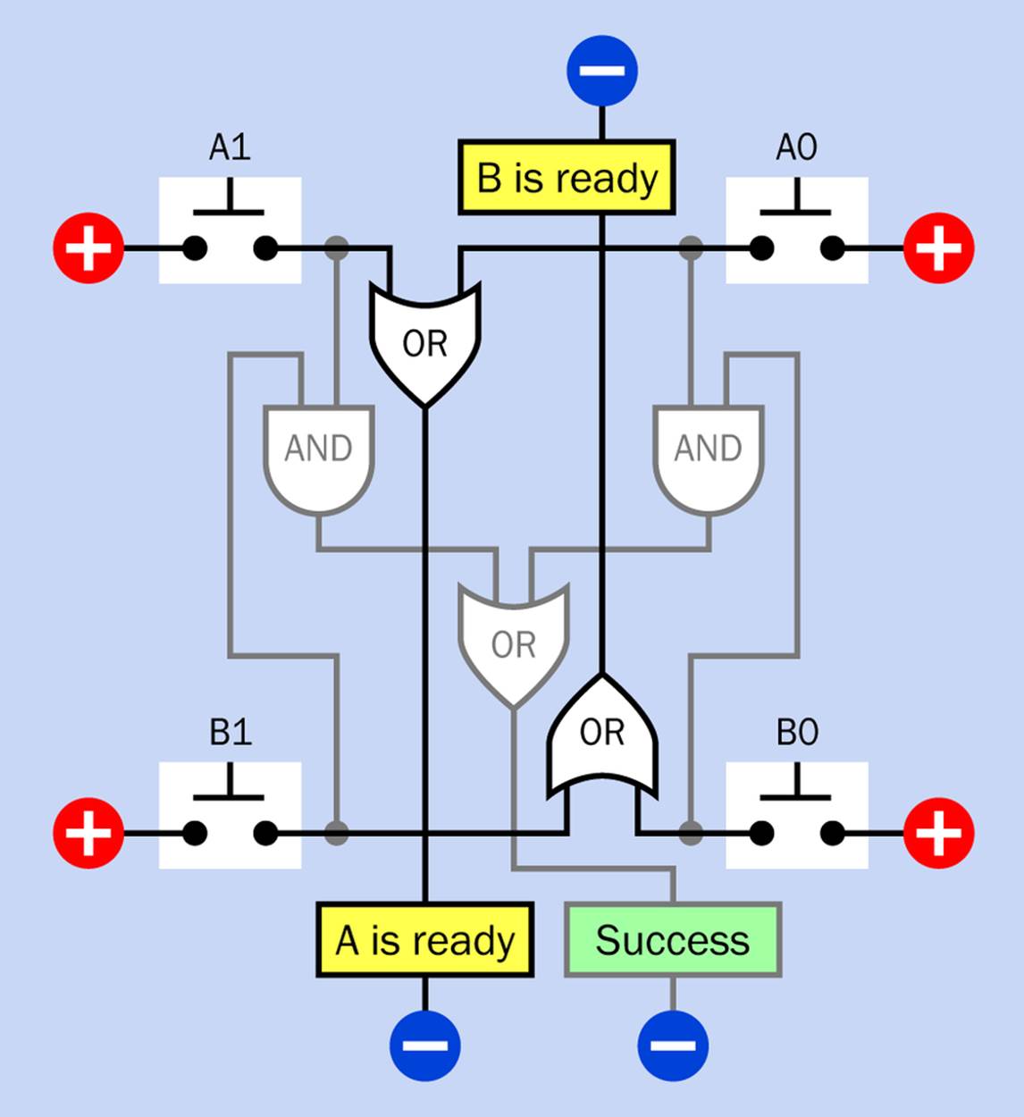
Figure 16-2. The previous two logic diagrams are shown here combined, sharing each pushbutton output between inputs on two separate logic gates. Unfortunately, combining multiple logic diagrams quickly results in complexity, which is difficult to interpret. In an effort to provide some clarity, connections from the previous logic diagram are shown here in gray.
Cheating Revealed
What about the “Cheat” indicator? It can be described like this:
“If A0 AND A1 are being pressed, then an indicator shows that Annabel is cheating. If B0 AND B1 are being pressed, then an indicator shows that Boris is cheating.”
Figure 16-3 shows this as another separate logic diagram. Once again, this can be combined with the other diagrams by sharing the output from each pushbutton among multiple logic gates.
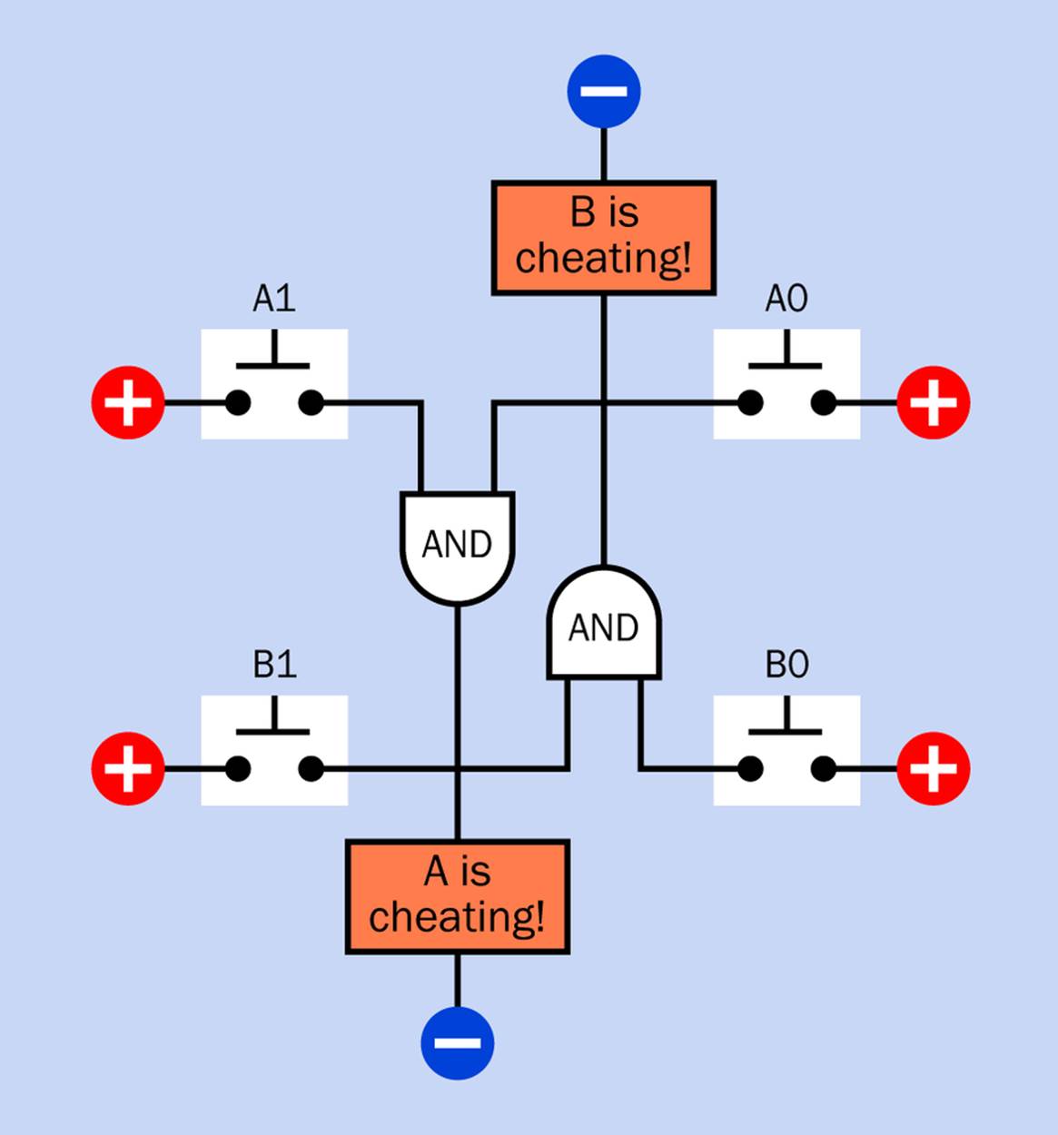
Figure 16-3. By adding two AND gates, we can see if either player has cheated by pressing two buttons at once.
Failure Indicated
Lastly, the “Fail” indicator. If the players press buttons that are not opposite each other, the test is a failure. Well, this can be displayed easily. We can describe it like this:
“If A0 AND B1 are pressed, OR if A1 AND B0 are pressed, then the players fail.”
Figure 16-4 shows a logic diagram representing this statement.
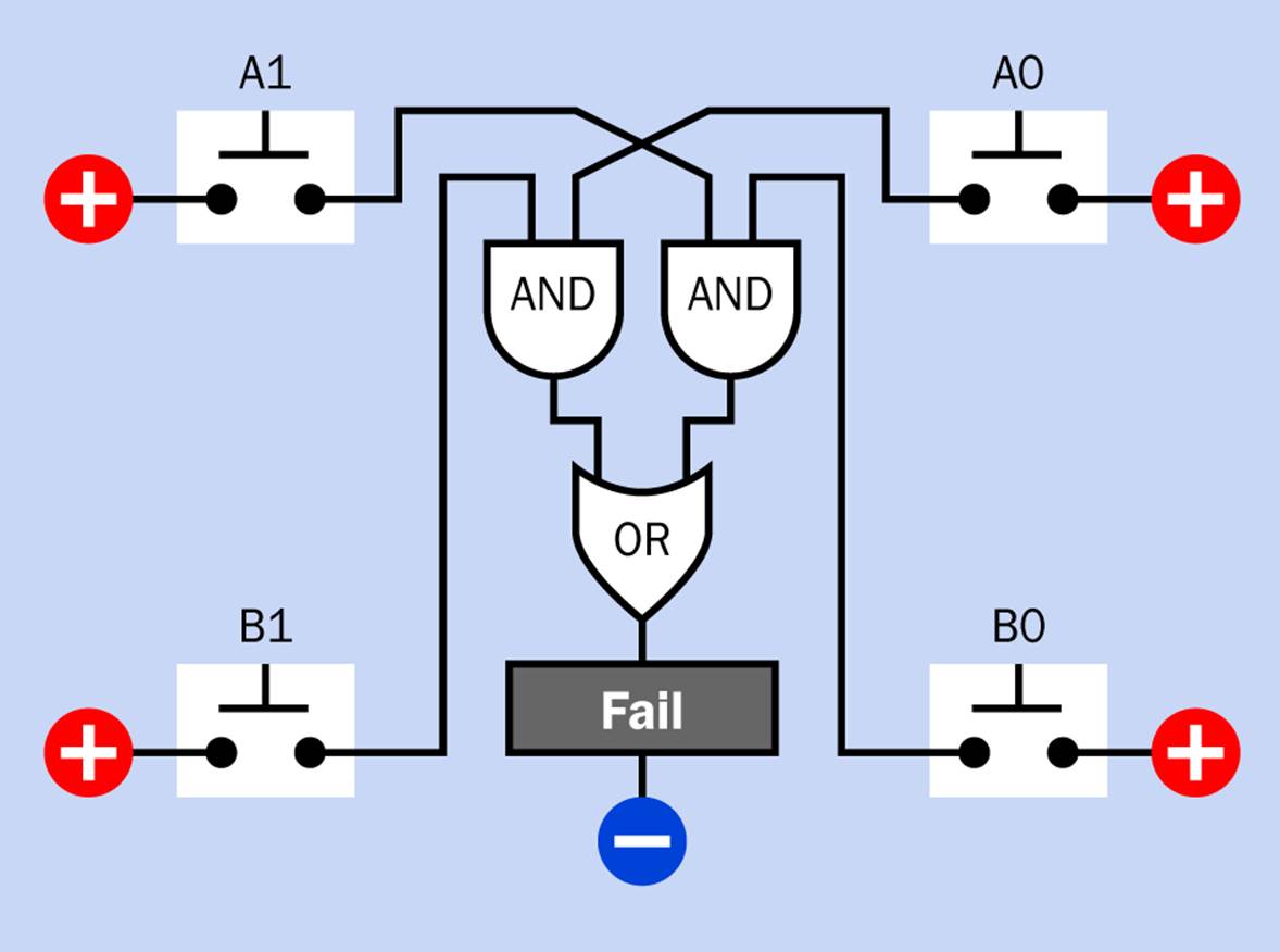
Figure 16-4. A couple more AND gates, feeding into an OR gate, will show if either of the incorrect button combinations is pressed.
Would you like to add this functionality to the breadboarded circuit in Figure 15-8? You may have noticed that there were several gates in the chips in that schematic that were not being used. Because every gate operates independently of the others in a multigate chip, we could make use of unused gates to provide the initial features that I have described above. For instance, the “ready” test requires just two OR gates, and there are three OR gates inside the 74HC32 chip that are not being used.
I’m tempted to say, “Sure, go ahead, add the new features!” But maybe you’d better not, because I don’t want you to get mad at me if you take time to build something that doesn’t work properly. And the fact is, if you add the features I just described, they won’t work properly. I can prove this by asking you to try a little thought experiment.
Conflicts
Suppose that Boris cheats by pressing B0 and B1 simultaneously. At the same time, Annabel is playing by the rules, so she presses only one button, A0. What happens?
Buttons A0, B0, and B1 are all being pressed. Because B0 and B1 constitute cheating, the “Cheat” indicator comes on, as it should.
But wait—Annabel is pressing A0. Because A0 and B0 are both being pressed, the “Success” indicator comes on!
This is not all. Because B1 and A0 are also being pressed, the “Fail” indicator comes on. And because each player has pressed at least one button, both of the “ready” indicators lights up.
This is a catastrophe. All the indicators come on!
What went wrong? The problem was that my descriptions were inadequate. I only thought about the buttons that have to be pressed to create a logical output. I didn’t consider which buttons must not be pressed to create that output. For example, I began describing the “ready” logic like this:
“If button A0 OR A1 is pressed, then an indicator tells Boris that Annabel is ready.”
But I should have written it like this:
“If button A0 OR A1 is pressed, AND neither B0 NOR B1 has been pressed yet, then an indicator tells Boris that Annabel is ready.”
In other words, I have to make sure that Boris hasn’t pressed one of his buttons yet, before the system tells him that Annabel is waiting for him to press one of his buttons.
Similarly, the “Success” indicator or the “Fail” indicator should only light up if neither A NOR B has cheated.
Hmm, that NOR word has turned up twice, now. Evidently I am going to have to use a NOR gate here, somehow, and this is all starting to look extremely complicated. Who would have thought that such a simple game could create unexpected issues? I think a chart will help to untangle the confusion.
The Untangling
Take a look at Figure 16-5. This now takes into account the buttons that are not being pressed, as well as the buttons that are being pressed. A0, A1, B0, and B1 represent the four buttons, with red meaning that a button is pressed, and black meaning that a button is not being pressed. A gray button with an X in it means that its state doesn’t matter because it is irrelevant to this particular logic test. On the right are the messages that should be created by each combination of buttons. Remember, the black (unpressed) button states are just as important now as the red (pressed) button states.
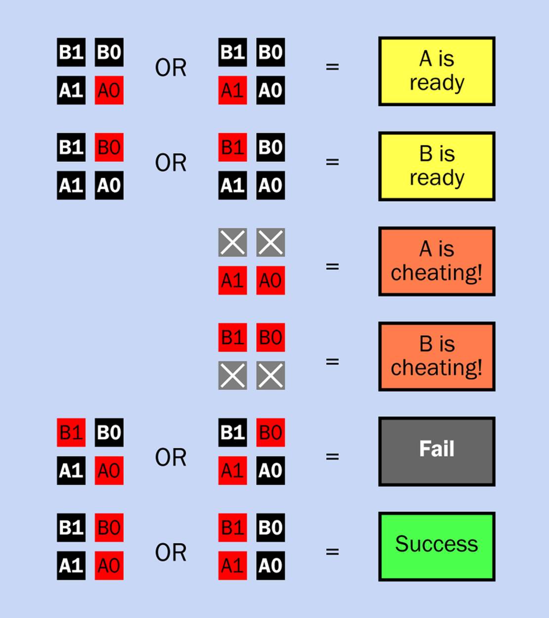
Figure 16-5. In this chart, A0, A1, B0, and B1 indicate a button that is pressed (red) or not pressed (black). A gray X means that in that particular test, the state of the button is irrelevant and can be ignored. The colored boxes on the right represent the indicators that should light up in response to each combination of buttons.
On the first line, Boris should only see a “ready” light for Annabel if Annabel has pressed one button (not both, which would be cheating), AND Boris has pressed neither B0 NOR B1.
The second line uses this same logic for Annabel’s “ready” light.
In the third and fourth lines, if someone is cheating by pressing both buttons, we don’t care what the other person is doing.
The “Fail” indicator and the “Success” indicator will light up only if those specific red-colored buttons are pressed, but other buttons are not being pressed.
Translating the Chart
Perhaps you’re wondering if there is still some other button combination that will have consequences that I haven’t predicted. No, the chart in Figure 16-5 specifies an outcome for every possible button combination. (If three or four buttons are pressed simultaneously, these combinations are all covered by the “Cheating” test.)
Now I can translate each line of the chart into a logic diagram, and this time, I feel confident that it will work. However, I will require two additional types of gates, to do this: NOR and XOR. In case you don’t recall how they function, you can check back to Figure 15-5.
Describing them in words, the NOR and XOR gates work like this:
§ The NOR gate has a low output if either or both of its inputs are high. The output only goes high if both of its inputs are low.
§ An XOR gate has a low output if both of its inputs are high or low. The output only goes high if either of its inputs is high while the other is low. (XOR stands for “exclusive-OR,” in case you were wondering. It is pronounced “ex-or.”)
In Figure 16-6 you can see how these gates are used to imitate the tests shown in Figure 16-5.
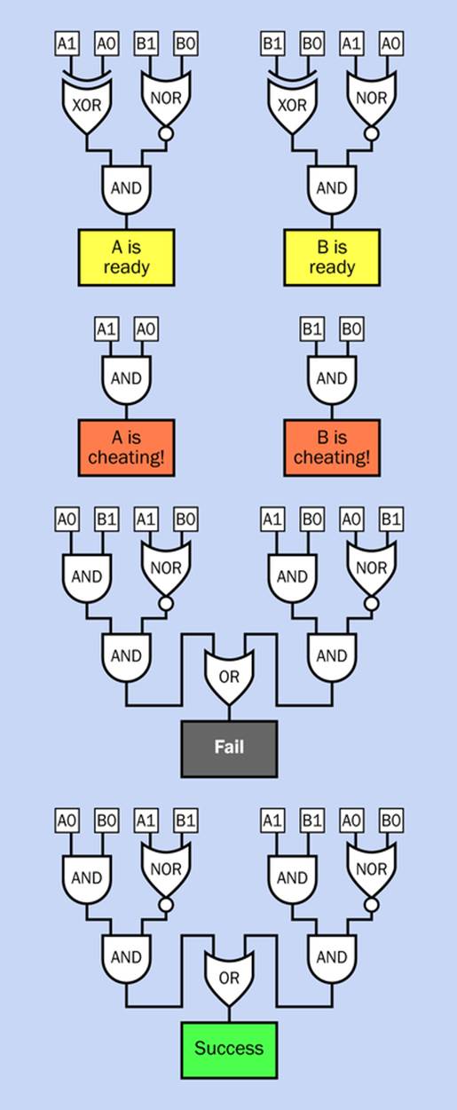
Figure 16-6. Logic diagrams that emulate the relationships shown in the previous figure. Each of the logic inputs (A0, A1, B0, B1) represents a connection with a pushbutton that can be pressed or not pressed and will provide a high input when it is pressed, while a pulldown resistor (not shown) will provide a low input when the button is not pressed.
In Figure 16-7 I have selected four possible button combinations as samples to see how they work in the logic diagram that decides whether the “A is ready” indicator should light up. In the lower two combinations, the “ready” indicator is not illuminated.
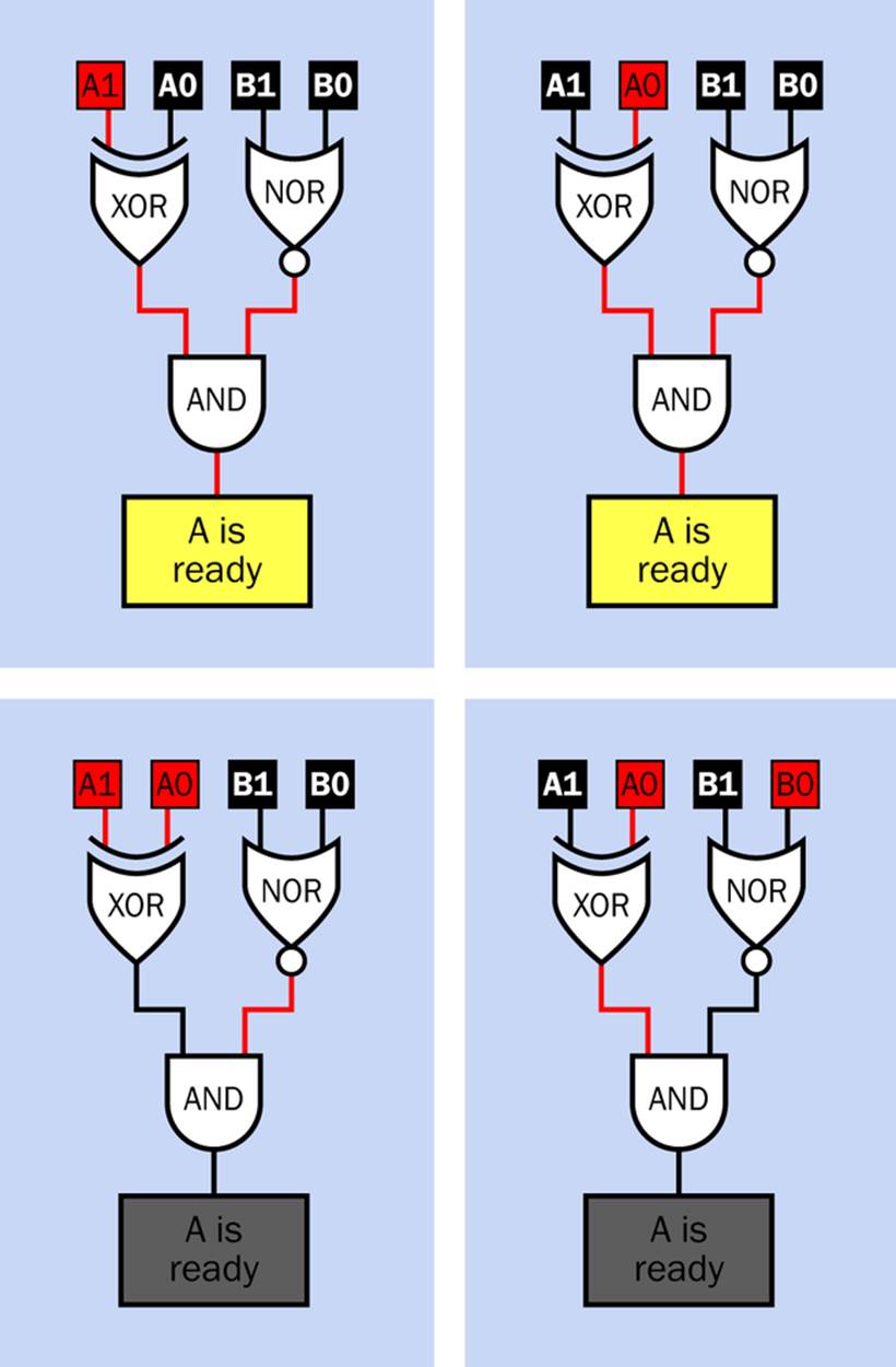
Figure 16-7. The results of four arbitrary combinations of the pushbuttons, for the “ready” test for Player A.
The diagrams in Figure 16-6 can be summarized in words like this:
§ Testing for “Player A is ready”: if either A0 or A1 is high (not both), AND neither B0 NOR B1 has been pressed yet, the “A is ready” indicator lights up.
§ Testing for “Player B is ready”: if either B0 or B1 is high (not both), AND neither A0 NOR A1 has been pressed yet, the “B is ready” indicator lights up.
§ Testing for “Player A is cheating”: if A1 AND A0 are both pressed, the “A is cheating!” indicator lights up.
§ Testing for “Player B is cheating”: if B1 AND B0 are both pressed, the “B is cheating!” indicator lights up.
Now things get slightly more complicated:
§ Testing for a “Fail” situation: if A0 AND B1 are both pressed, AND neither A1 NOR B0 has been pressed, then the “Fail” indicator lights up. OR, if A1 and B0 are both pressed, AND neither A0 NOR B1 has been pressed, then then the “Fail” indicator lights up.
§ Testing for a “Success” situation: if A0 AND B0 are both pressed, AND neither A1 NOR B1 has been pressed, then the “Success” indicator lights up. OR, if A1 and B1 are both pressed, AND if neither A0 NOR B0 has been pressed, then the “Success” indicator lights up.
These statements are derived from each pattern of button presses shown in Figure 16-5. If you read the statements aloud to yourself while looking at the button-press symbols, you’ll see that they match, one-for-one.
Now you could build the circuit. You would assemble enough chips to provide all the necessary gates and carefully link each button with the various appropriate inputs of the gates. Remember, it’s quite okay to connect one button to several gate inputs.
The trouble is, this has turned into a much larger project than you might have expected. To provide all the logic gates shown in Figure 16-6 you would need three quad two-input AND chips, one quad two-input OR chip, two quad two-input NOR chips, and one quad two-input XOR chip. That’s seven, altogether. They would not all fit onto a breadboard.
Hm. Can it be simplified, somehow? Well, actually, yes, it can. We can think of this as “optimizing” the logic.
Optimizing
Remember earlier I said that the “cheating” condition should override everything else? This idea can be used to simplify things. What I’m thinking is this: if either Annabel or Boris is cheating, we don’t even have to think about “Success” or “Fail” outcomes. We just light up the “Cheat” indicator and prevent any other indicators from being illuminated, and that’s the end of it.
The way to do this with logic gates is to have a cheat-detection section, and if there is no cheating, it sends an “okay” signal to the success/fail section. The “Success” and “Fail” lights cannot come on without the “okay, no cheating” signal. I’ve illustrated this concept using a flow diagram in Figure 16-8. In this diagram, we have to make sure that neither A NOR B is cheating before the “okay” signal leads us down to see whether the trial is a success.
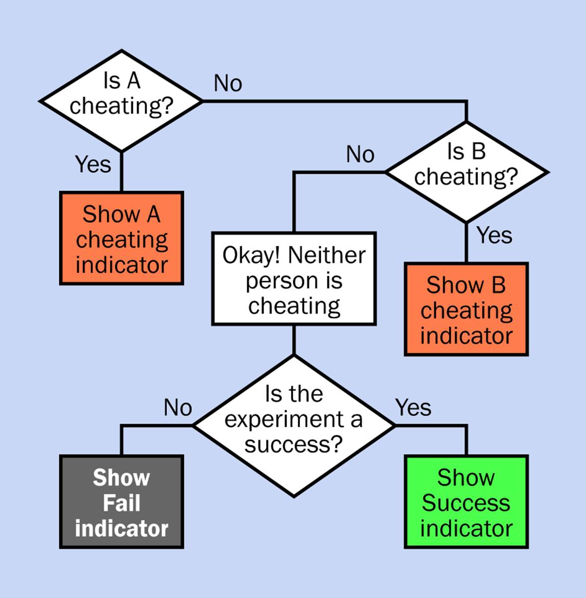
Figure 16-8. A flow diagram shows the concept of verifying that no cheating has occurred, before we determine whether the outcome is a success or a fail.
How can we translate this into logic gates? Well, a NOR gate gives a high output if, and only if, both of its inputs are low. If we use a low input to mean that a person isn’t cheating, the output from the NOR gate will be high so long as neither person is cheating.
In the lower section of Figure 16-9 you see a NOR gate added, tapping in to the “cheating” indicators for A and B. So long as NEITHER Annabel NOR Boris is cheating, the NOR gate gives a high output. This is added to some three-input AND gates, which require all their inputs to be high before a “Success” or “Fail” indicator can light up. This is the same as saying that if either player cheats, the “Success” and “Fail” indicators won’t light up.
To accommodate the three-input AND gates, I also had to rework the logic at the bottom of the diagram, using four XOR gates. I leave it to you to figure out why they should work. Just refer back to Figure 16-5.
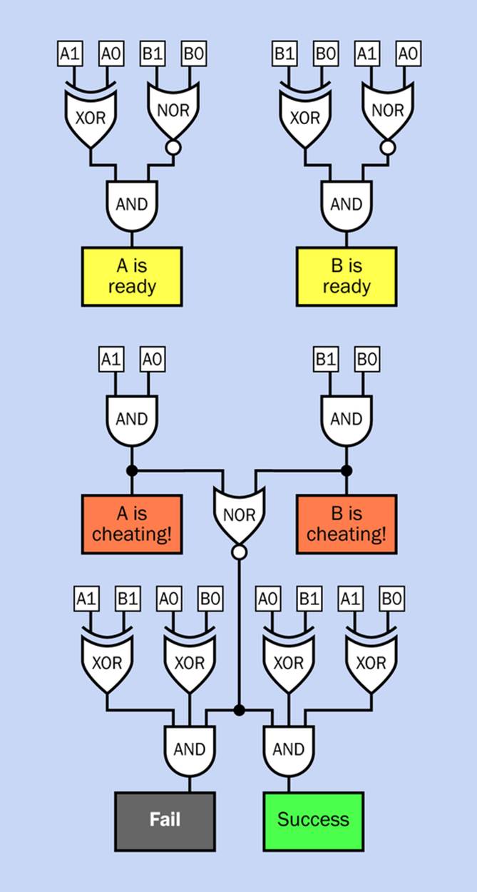
Figure 16-9. A simplified version of the previous logic diagram adds a NOR gate, which must give a high input, meaning that neither A NOR B is cheating, before the “Success” or “Fail” indicator can light up.
Perhaps you are wondering—what is the system for simplifying or optimizing a logic diagram? The formal way to do it is by learning proper Boolean notation and looking for functions that duplicate or contradict each other. There’s an example of this kind of thing onWikipedia, but I find it difficult. I prefer just to stare at a logic diagram while imagining all of its possible states and trying to see other ways to satisfy the requirements. Once I think I have a simplified version, I check every combination of inputs to make sure that they all work. This is an intuitive approach, not the classical approach, but it works for me.
Building It
Now that the circuit has been optimized, you can build it. You will need one quad two-input AND chip, one triple three-input AND, one quad two-input NOR, and two quad two-input XORs. That’s just five chips instead of seven. (I managed to get rid of the OR chip entirely.)
The pinouts of the additional chips are shown in Figure 16-10 and Figure 16-11. Notice that the NOR gates, inside the chip, are inverted compared with AND, OR, and XOR gates inside their chips. Be careful when making connections.
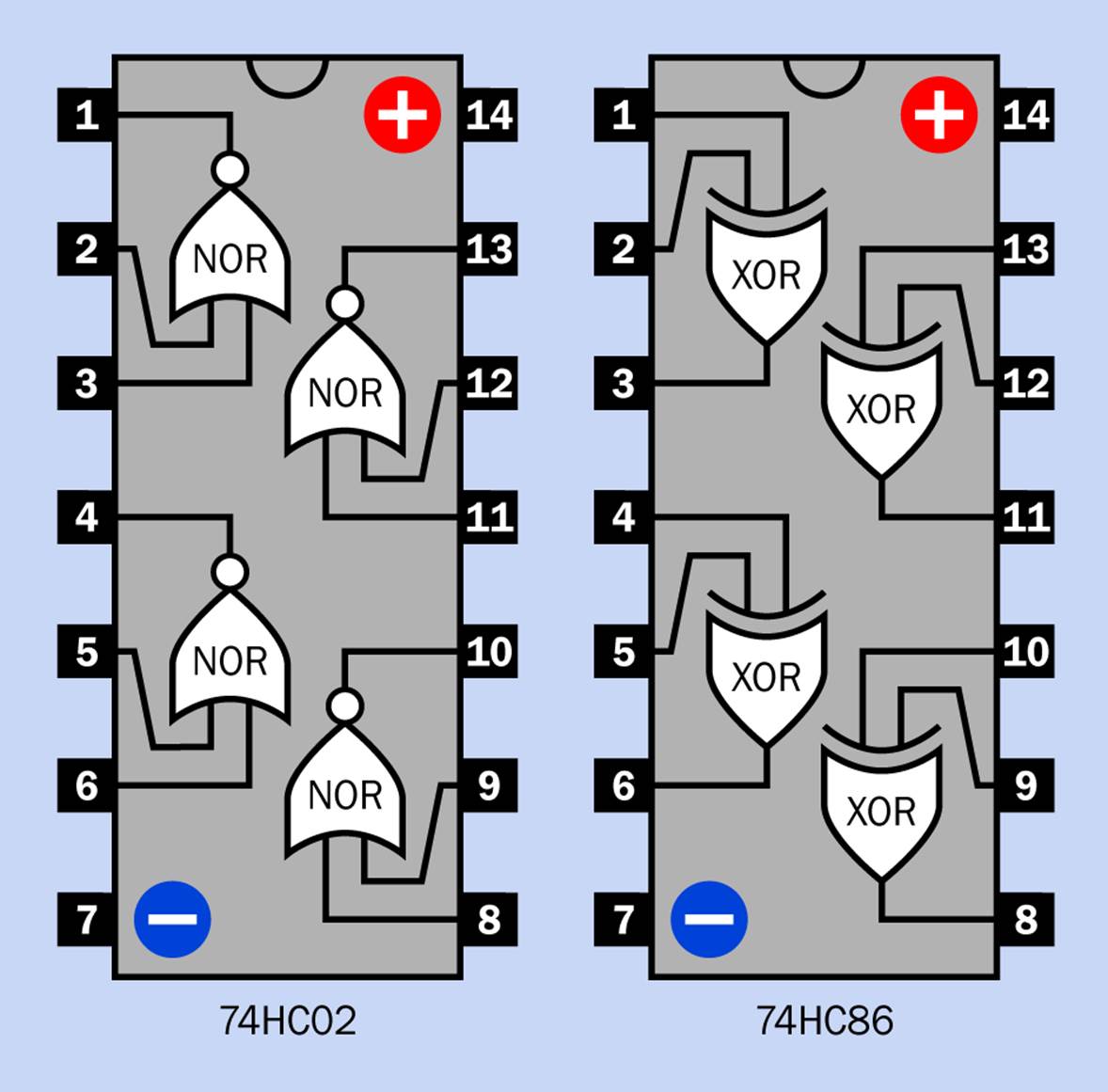
Figure 16-10. A 14-pin logic chip can contain four two-input NOR gates or four two-input XOR gates in the configurations shown here. It’s important to remember that the inputs and outputs of the NOR gates are inverted compared with the gates inside other quad-two-input chips.
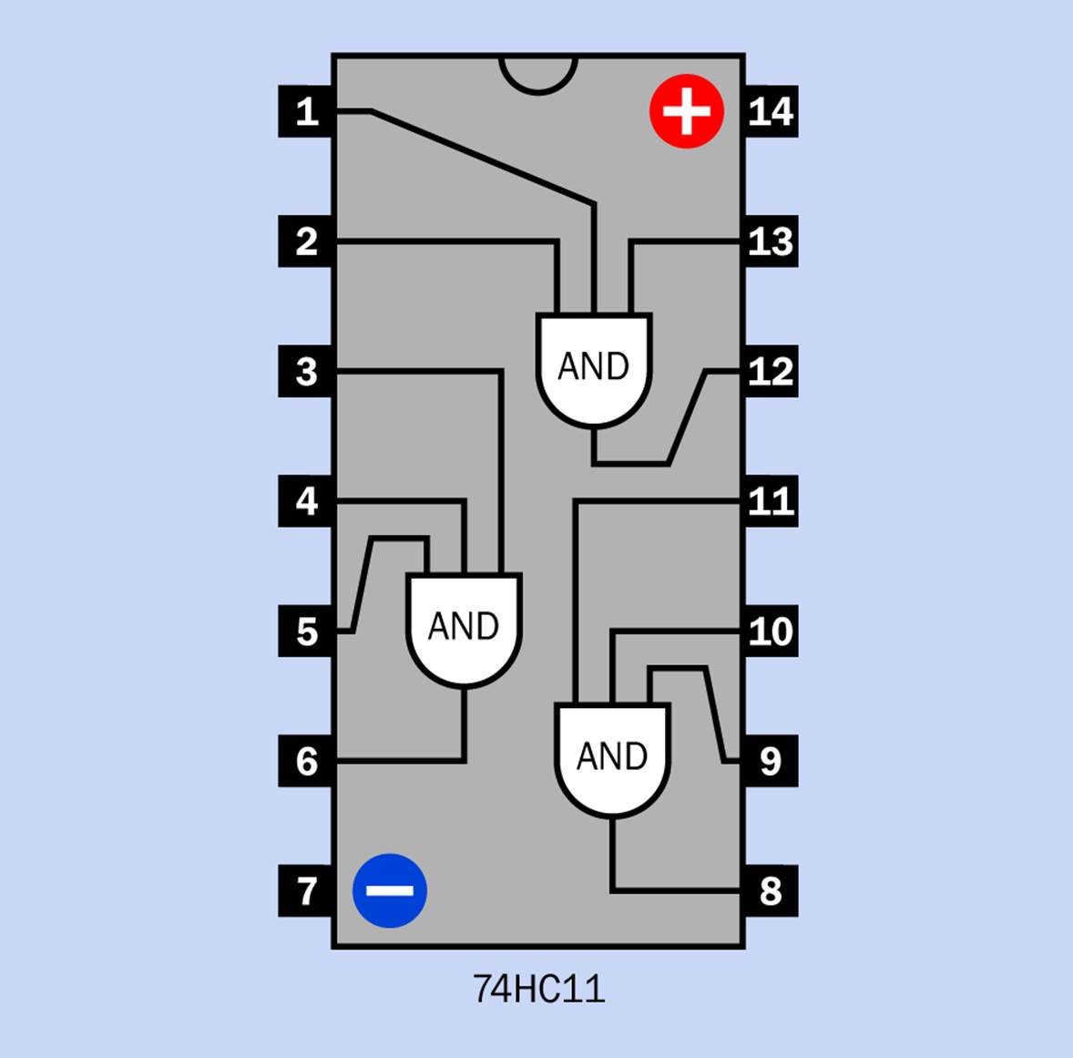
Figure 16-11. A 14-pin logic chip can contain three three-input gates, as shown here.
You can see how everything is wired together for a breadboard layout in Figure 16-12. XOR gates have an X in them, AND gates have an & sign, and NOR gates are represented by letter N. (These are not standard abbreviations.)
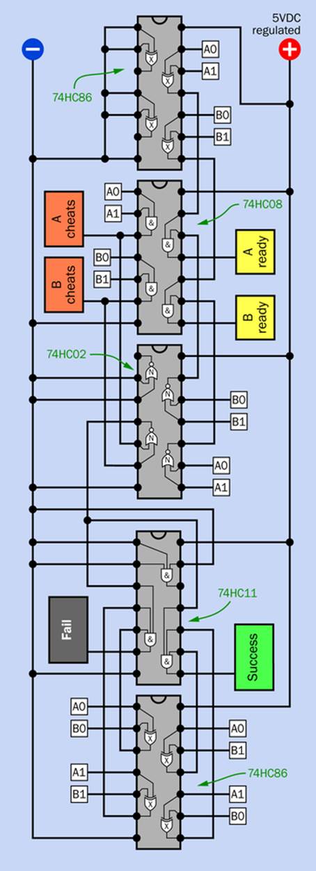
Figure 16-12. The final schematic for the Telepathy Test, using five logic chips.
Because the schematic in Figure 16-12 barely fits within one printed book column, I had to leave out the pushbuttons (which you are likely to mount separately anyway). They are shown in Figure 16-13. The output from each button goes to five button labels. You need to connect each of these labels to an identical label in Figure 16-12. Thus, the first A0 label in Figure 16-13 can connect with the A0 label in the XOR chip at the top of Figure 16-12, and so on. The easiest way to accomplish this is with a multicolor ribbon cable.
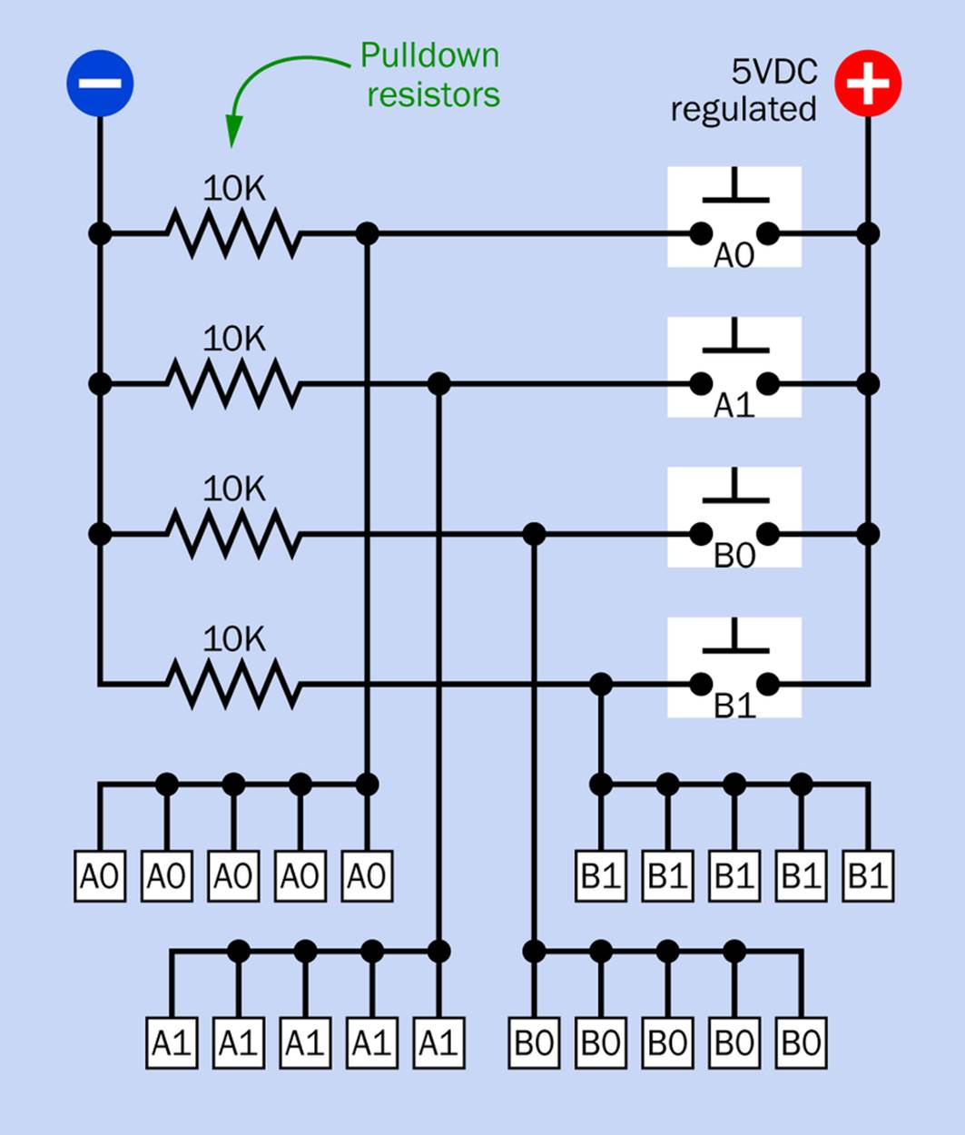
Figure 16-13. Four SPST normally-open pushbuttons should be used in conjunction with the ESP Test circuit. The output from each of them is distributed among five chips. Because each group of five button-inputs is high or low simultaneously, one pulldown resistor will be sufficient for each group.
Probably you would also mount the LED message indicators separately. Just be careful to add a 220Ω series resistor for each LED, to avoid overloading the outputs from the logic chips (unless you are using LEDs that contain their own series resistors).
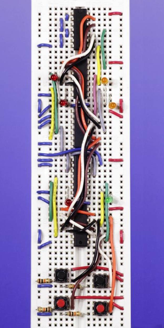
Figure 16-14. A breadboarded version of the complete Telepathy Test, using five logic chips. Six LEDs provide outputs that are identified in the schematic of the circuit. No series resistors are shown because I chose the type of LED that contains its own series resistor. The two pushbuttons for Player A are the red ones at the bottom. The buttons for Player B are the black ones, immediately above. This configuration of the circuit is only for demonstration purposes. For a functional Telepathy Test, the buttons would be located separately so that the players would be unable to see each other’s choices.
In Figure 16-14 you can see a breadboarded version of this circuit. After I made the connections between the five chips, I realized there was still just enough space at the bottom of the breadboard for four tactile switches, so I put them there and connected each of them to its respective logic inputs. There was no space to locate the wires from the switches along each side of the board, so I ran some of them down the middle.
Details
You should be careful that the LEDs that you use as “Cheat” indicators (the orange rectangles in the schematic) don’t affect the voltage output from their AND gates too much. The outputs from these AND gates don’t just supply the LEDs; they also connect with the inputs of NOR gates in the next chip. Each of these inputs must be at least 4V when there is a high output from the AND gate supplying it. An LED may pull down this voltage, so be sure to check it with your meter.
If you decide to build a fully-functional version of this circuit instead of just a breadboard demo, you will need two copies of each “Success” and “Fail” LED—one for each player. To control the load of two LEDs driven in parallel, you can increase the series resistor or amplify the chip outputs. The easiest way to amplify the outputs is to pass them through the transistor pairs in Darlington array such as the ULN2003 chip. Darlingtons that can amplify seven or eight inputs are readily available.
Alternatively, you can drive each pair of LEDs in series. The advantage of this plan is that none of the power from the logic chip is wasted in a resistor. Unfortunately the results are difficult to predict, because LEDs are more sensitive to current than to voltage, and different LEDs have very different specifications. Be sure to measure the current passing through LEDs when they are wired in series, and add a small resistor if you find that the LEDs are drawing more than their rated current.
I really encourage you to build this circuit. It’s quite easy, because very few components are involved. The only requirement, really, is to be careful and precise in making connections. I think you can do that if you decide to give it a try.
If you actually use a version of this circuit, bear in mind that one player’s actions may not be entirely random, and the other player may learn this pattern—even if the first player is unaware of it. This takes us into the realm of randomicity, which I will be dealing with later.
The Digital Difference
A superficial inspection of the schematic in Figure 16-12 shows that it looks very different from the schematics in the experiments that involved op-amps. For a start, there are no capacitors, and the only resistors are for pulldown purposes. No transistors, either! This is because logic chips have been designed to talk to each other without any help from other components. So long as you use chips from the same family, the output from one is guaranteed to be acceptable to the input of another.
You can also share the output from one gate among the inputs of several other gates. For instance, the output from the lower-left NOR gate in the 74HC02 chip in Figure 16-12 is shared by the inputs of two AND gates below. Driving multiple gates from one output is known as fanout, and the HC series should allow a single logic output to be shared among as many as 10 logic inputs.
Making It Even Better
Now, could the schematic be optimized still further? Probably. I’m thinking that instead of testing separately for “Fail” and “Success,” I could use logic that basically says: if the central NOR gate says that neither player is cheating, and two buttons have been pressed, and we don’t have a “Fail” condition, then we must have a “Success” condition. In other words, “Success” could be defined as “NOT Fail.”
However, my head is starting to ache from trying to figure all this out, so I will not attempt to optimize the circuit any further. You should give it a try yourself, though, if logic interests you. If you succeed in reducing the chip count from five to four, please let me know. But don’t try too hard, because after the next experiment, I’m going to show you how the number of logic chips can be reduced to just two, if we add one extra component called a decoder. Stay tuned!
Not So Simple?
When you started reading about the Telepathy Tester, maybe you thought it was too simple to be interesting. But now maybe you’re feeling that it became too complicated to be interesting! Well, okay, once again, you don’t have to wrestle with it if you don’t want to. Hold on to the conclusions we reached, though, because they are recurring facts of life in digital circuits:
§ A logic problem which looks simple at first can become extremely complicated when too many extra tests and conditions are added. Logic conflicts can occur. It’s easy to imagine new features that would be nice to have—but think twice before you try to add them.
§ User input is always a problem, because we have to imagine every possible quirk of human behavior that may occur, and process it appropriately.
§ There are systematic ways to build a logic circuit, but they will not create the simplest possible circuit with the lowest chip count. Optimizing can almost always reduce the chip count—but on the other hand, it can create a circuit that is more difficult to understand, more likely to contain errors, and perhaps more difficult to modify subsequently.
Desktop computers have always used microprocessors, but logic chips were needed in addition, and the number of chips (the “chip count”) was a big deal, because chips weren’t cheap in those days. The Telepathy Test shows you the kind of design process that the computer pioneers went through. Even today, people who design CPUs are still dealing with logic states—but their task has become easier because they not only have better design tools, but powerful simulation software to test everything.
Could We Use a Microcontroller?
Well, could we? Of course the answer is yes, absolutely, yes! Each button would connect with an input to the microcontroller, and you would write program code to look for different patterns of button-presses. IF-THEN statements would then branch to different outcomes.
Logic errors would still be possible (actually, they would be probable) but overall, the design process would be much less of a headache, and the hardware would become trivial. Instead of fifteen logic gates in five logic chips, you would just need one microcontroller. If someone asked me to build a Telepathy Tester tomorrow, I have no doubt that I would use a microcontroller.
However, my purpose here is to show you how stuff works. Logic is absolutely fundamental in all digital devices, and the best way to learn about it (as always) is with hands-on involvement. For that purpose, there’s no substitute for those old logic chips.
Although, actually—there are two possible substitutes. As I just mentioned, there is the possibility of using a decoder, which contains multiple logic gates, so that you don’t have to wire so many gates together yourself. I’ll get to that in experiments 19 and 20.
The other possibility is to replace each logic gate with nothing more than a pair of old-fashioned electromechanical switches.
I’m going to show you a game circuit, next, which can be built from switches—although you will see that it can still be built from chips, or even a combination of switches and chips, if you prefer.
All materials on the site are licensed Creative Commons Attribution-Sharealike 3.0 Unported CC BY-SA 3.0 & GNU Free Documentation License (GFDL)
If you are the copyright holder of any material contained on our site and intend to remove it, please contact our site administrator for approval.
© 2016-2026 All site design rights belong to S.Y.A.