Make: More Electronics (2014)
Chapter 19. Experiment 19: Decoding Telepathy
Take a look at Figure 19-1, where I have redrawn the Telepathy Test logic diagram using a decoder chip. Although this circuit now incorporates every possible feature that I talked about earlier, it requires only three chips. A circuit doesn’t get much simpler than this.
Decoder Testing
So what is this mysterious component that makes everything so simple? Before you build the circuit, let’s start by bench-testing a decoder. The one I’m recommending is the 74HC4514. I’m specifying the HC family because whenever I buy a chip, I’m thinking that I might reuse it for some other purpose in the future, which may require it to power LEDs (at least while testing the circuit). Remember that the 74HC00 chip series can source or sink up to 20mA, while the output from a 4000 series chip is much more limited.
However, the 74HC4514 is relatively expensive (more than $3 when bought singly), and you should know that its cousin, the old CMOS version, which is simply numbered 4514, is more widely used and cheaper. For this experiment, because the decoder isn’t going to drive any LEDs, either of the chip versions will work. They have the same pinouts, as shown in Figure 19-2.
Connect the chip as shown in Figure 19-3. At the top of the schematic, I’m specifying switches instead of pushbuttons to test the chip, because you may find it inconvenient to hold down two or three buttons simultaneously. However, either switches or pushbuttons will work. The breadboarded version is shown in Figure 19-4.
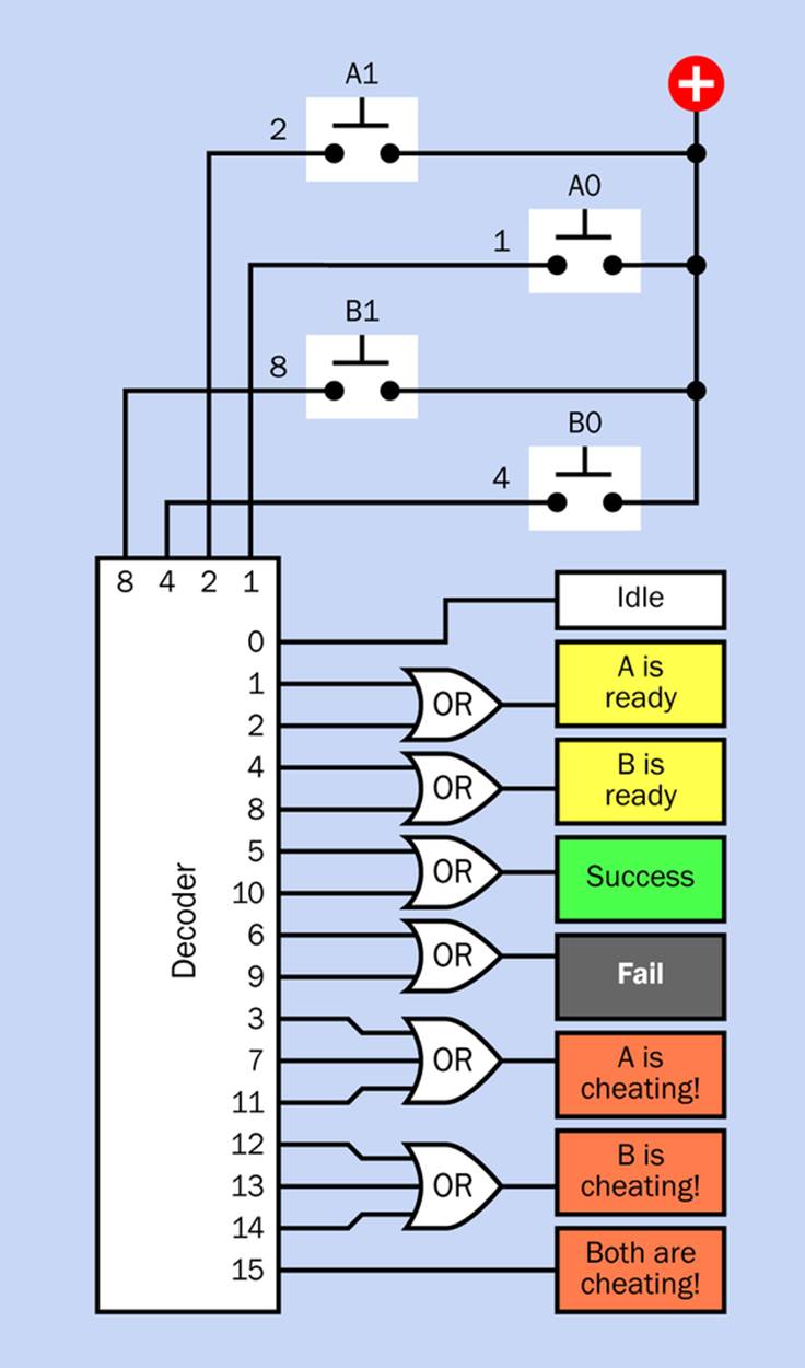
Figure 19-1. Using a decoder chip, the number of logic gates in the Telepathy Test project has been radically reduced. Pin locations on the actual chip have been reshuffled here to reduce wiring crossovers in the diagram.
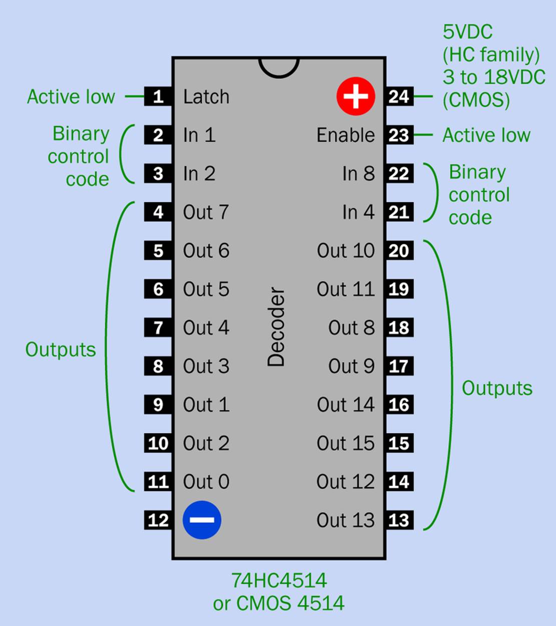
Figure 19-2. Pinouts of the decoder chip that can simplify the Telepathy Test project.
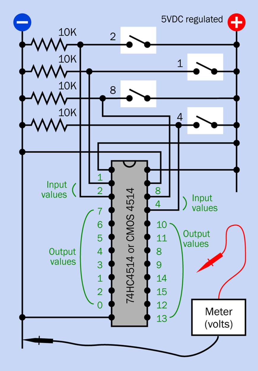
Figure 19-3. Setting up the encloder chip for exploratory testing. The meter probe can be touched against any of the unconnected pins. See text for additional details.
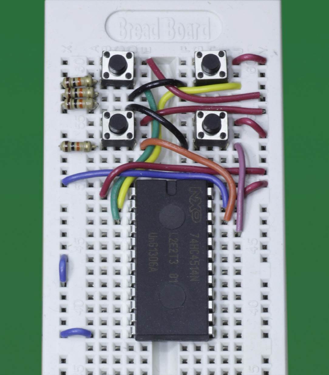
Figure 19-4. The breadboarded version of the decoder test circuit. Decoder chips from some manufacturers may be narrower than the one shown here, but the functionality is the same.
Set your meter to measure DC volts, and connect the negative probe to the negative bus, using a jumper wire with alligator clips at each end or a minigrabber on your meter probe. You will be touching the other, positive meter probe to the pins of the chip that are shown as outputs in the diagram.
Because the chip performs simple arithmetical calculations, its pins have values asssigned to them, as shown in the figure. The input pins have values 1, 2, 4, and 8. These numbers are also shown beside the switches that supply power to the inputs. The output pins have values 0 through 15. You’ll see that they are not in numerical order (this is not a typographical error in the figure). To avoid confusion, you may want to write the numbers on adhesive labels that you stick to the breadboard beside the chip (if you can write small enough, with a fine-tip pen).
Begin with all of the switches open. Run the meter probe along all the output pins of the chip, and you should find that the output pin with value 0 is high, while all the others are low. Now close switch 1, and the output pin with value 1 will be high, while all the others are low. Now close switches 1, 2, and 4 simultaneously, and keep them closed. You will find that output pin with value 7 is now high, while all the others are low.
The decoder is functioning like a little adding machine. The values of input pins that have a high state are summed together. The chip then energizes the output pin that has the corresponding value.
Here’s the most important feature of a decoder chip:
§ The 1, 2, 4, and 8 input values are chosen so that each output value can only be created by one unique combination of inputs.
§ Therefore, the value of the output can tell us which switches have been closed.
In case this isn’t entirely clear, take a look at Figure 19-5, which shows four possible states of the chip, chosen at random. I have simplified the figure by showing inputs at the top of the decoder, in sequence, and outputs down the right-hand side of the decoder, in sequence. A red input indicates a high value, created by a closed input switch, while a red output also indicates a high value. If you add up the high values at the top, that gives you the value of the output pin that will be high.
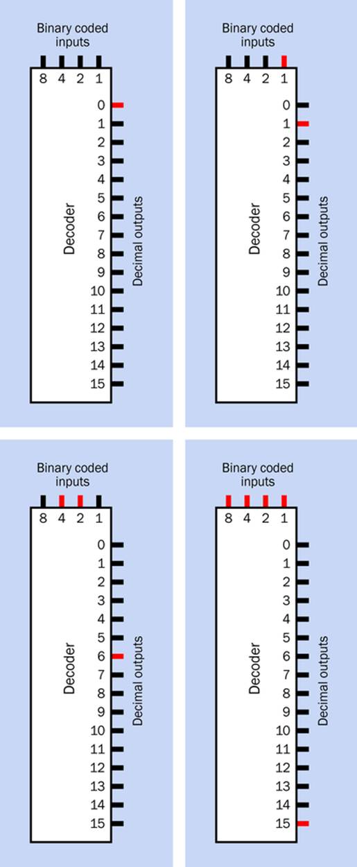
Figure 19-5. Four examples of the behavior of a decoder chip, which creates a high output (shown in red) on a pin whose assigned value is the total of the values of the input pins that have high states. Pins in this diagram have been sorted into numerical sequence to clarify the process. Pins on the actual chip are not arranged sequentially.
Remembering Binary
Now go back to Figure 19-1. This is almost the same as the diagram in Figure 19-5 except that I have moved and grouped the numeric values of the output pins so that they align conveniently with the logic gates.
In the Telepathy Test, we can now see easily which switches have been pressed or not pressed by Boris, and which switches have been pressed or not pressed by Annabel. For instance, if output pins on the decoder with values 1 OR 2 are high, switches A0 OR A1 (with values 1 OR 2) are closed, and all the other switches are not closed. Therefore, in the Telepathy Test, A has made a selection, while B has not done so yet.
Suppose the output pin with value 6 has a high output. This can only mean that switches A1 and B0 (with values 2 and 4) are closed, while the other switches are open. Similarly if the output pin with value 9 has a high output, this can only mean that switches A0 and B1 (with values 1 and 8) are closed, while the other switches are open. Therefore, if pins with value 6 OR 9 have a high output, each player has closed a switch, and the switches are not opposite each other, so A and B failed that particular telepathy test.
You can go through all the combinations and check the outputs.
In Figure 19-1, you will see that I added an extra output indicator, which says that both players are cheating when all four pushbuttons are closed. I also added an output which states that the circuit is “Idle” when no switches at all have been closed.
The inputs to the decoder are described as “binary” inputs because their values are the same as the place values in a binary number. I wrote about binary code briefly in Make: Electronics, so I’m just including one quick-reference diagram in Figure 19-6 to show the relationship between binary numbers and pin values on the decoder chip. It is called a “decoder” because it takes a number in binary code and decodes it to provide a single high state on a pin that can be identified with decimal notation.
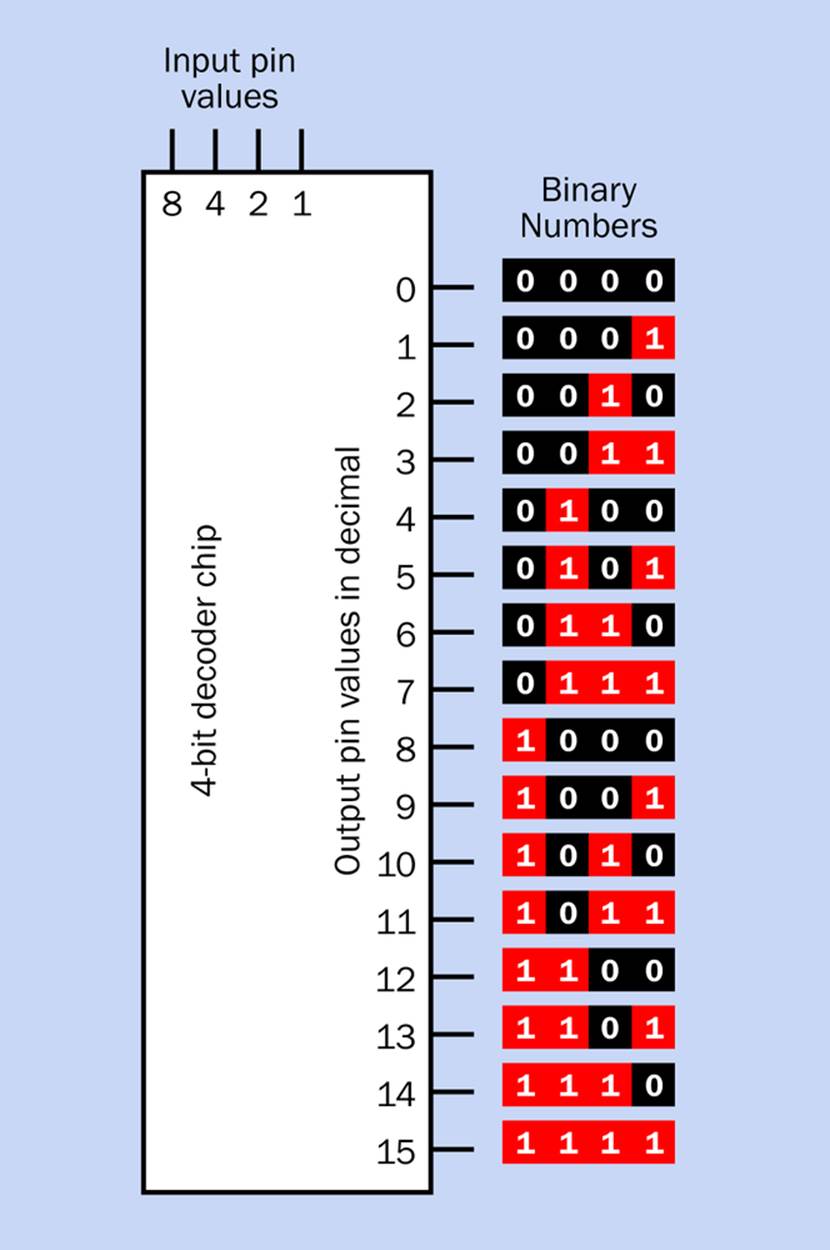
Figure 19-6. The high and low states of decoder input pins can be thought of as 1s and 0s in a binary number. The output pins of a decoder have the values of equivalent decimal numbers.
§ Because a binary digit is often referred to as a “bit,” and because the 74HC4514 decoder (or its older 4514 cousin) has four binary inputs, it is often referred to as a “four bit” decoder. It may also be described as a “4/16 decoder,” as it has four inputs and sixteen outputs.
Boarding It
The Telepathy Test is now very easy to build. The full schematic is shown in Figure 19-7. In this circuit, you can use either the cheaper CMOS version of the decoder (the 4514) or the more expensive HC version (the 74HC4514, which was developed to emulate the earlier 4514 with the same pinouts). Note that the old CMOS chips don’t have enough output power to drive LEDs directly. This is why I suggested that you should perform the initial test in this experiment with a meter, which draws negligible current.
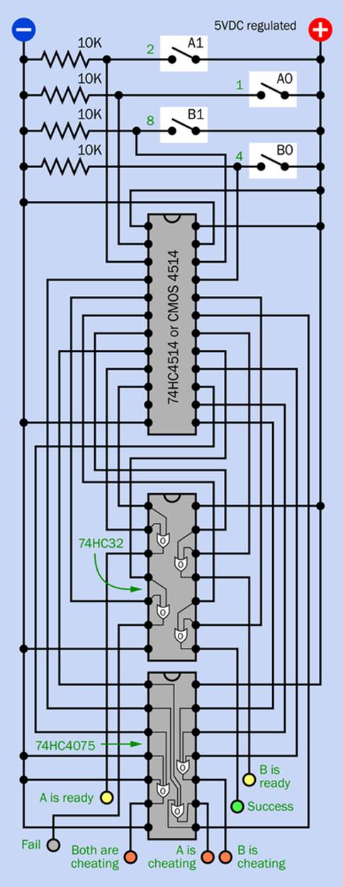
Figure 19-7. Schematic for the Telepathy Test using a decoder chip and two logic chips.
In the circuit shown here, you’ll need a quad two-input OR chip—the 74HC32, which you have used previously. Its pinouts are shown in Figure 15-7. The other logic chip is a triple three-input OR chip—the 74HC4075, which you have not dealt with before. Its pinouts are shown in Figure 19-8. The internal connections of this chip are similar to those of the triple three-input AND chip, which was shown in Figure 16-11. They are not exactly the same, however, and you should follow the schematic carefully when making connections.
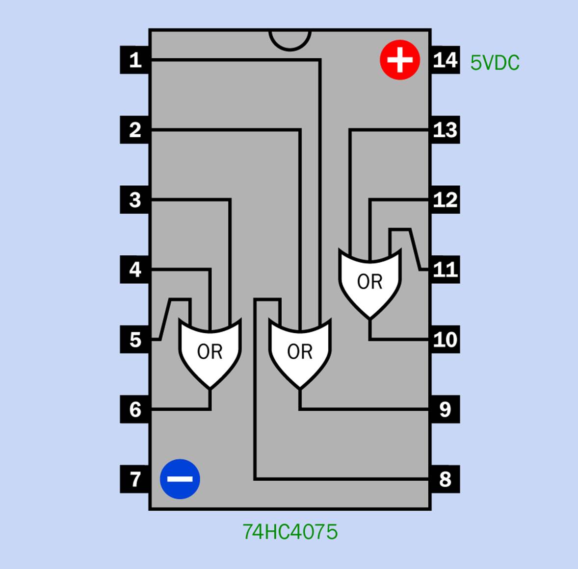
Figure 19-8. Internal connections of the three OR gates inside a 74HC4075 chip.
If you refer back to Figure 19-1, you’ll see that almost all the decoder outputs pass through logic gates before lighting an appropriate LED. If we use 74HC00 series logic gates, these will be powerful enough to light the LEDs. But what if you choose to use the cheaper 4000 series decoder chip? Outputs with values 0 and 15 are shown connected directly to indicators.
You can get around this by omitting the “Idle” indicator that would be connected to output value 0, powering the “Both are cheating!” output from output value 15 by passing the signal through a third three-input OR gate (not shown in Figure 19-1). If you tie two inputs of a three-input OR gate to negative ground and apply a signal to the third input, the OR gate just passes the signal through. It acts as a “buffer,” with an output state that is always the same as the state of its one active input. This is shown in Figure 19-7.
All of the LEDs share a single series resistor. This is acceptable and sufficient because only one of the LEDs will be powered at a time.
When placing jumper wires, I suggest it’s a good idea to print a paper copy of the schematic in Figure 19-7 and apply colored ink to each line after you establish the corresponding jumper on the breadboard. This will reduce the risk of wiring errors, which tend to be common where multiple conductors are parallel and close together.
A breadboarded version of the circuit is shown in Figure 19-9. In it you will see that the decoder that I used is an extra-wide chip. Some versions of the 74HC4514 look like this, while others are normal width. The functionality is the same.
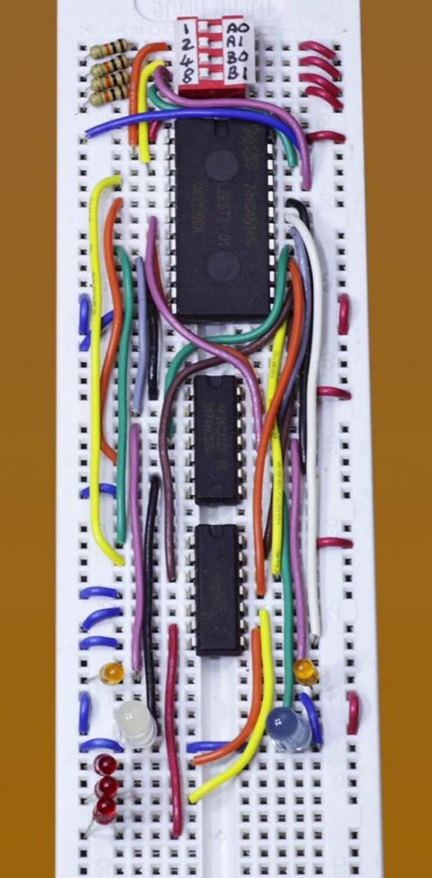
Figure 19-9. The Telepathy Test wired using a decoder to reduce the chip count and the complexity of the circuit.
Although the 4514 chip should work acceptably in this circuit, be cautious about mixing it with HC chips if you reuse it in some other circuit in the future.
Decoder Pinouts
Getting back to the pinouts of the 4514 and the 74HC4514, shown in Figure 19-2: there are two numbering systems here. The white numbers in the black rectangles are the standard pin numbers, which are applied to any chip. They always start at the top-left pin and proceed counter-clockwise around the edge of the chip. I will always refer to these numbers as “Pin 1,” “Pin 2,” and so on.
The numbers that I have added inside the body of the chip are the values that the pins represent when they have a high state. For instance, when Pin 22 has a high state, this represents an input of value 8. When Pin 20 has a high state, this represents an output of value 10.
A datasheet for this component will identify the functions of the pins in some other way, which is unfortunately not standardized. The input pins, for instance, may be labelled A0, A1, A2, and A3. Or, they may be identified as A, B, C, and D, or DATA1, DATA2, DATA3, and DATA4. Since there is such a lack of standardization, I felt it would be helpful to make the functions of the pins clearer by using my own scheme.
In datasheets, the output pins may be identified as Y0 through Y15, or S0 through S15, or similarly. I thought it was clearer to identify them as Out 0 through Out 15. (I often wonder why the people who create datasheets are so reluctant to use three letters—as in the word “Out,” for example—rather than just one letter.)
Going back to the pin-numbering scheme, there are a couple of chip features that I have not explained so far. Pin 1 is the Latch Enable pin, which is active low. In other words, when this pin is held low, it latches the output state and tells the chip to ignore any inputs until further notice. This is not a feature that we need in the Telepathy Test circuit, so the breadboard schematic shows Pin 1 tied to the positive side of the power supply. In datasheets, the Latch Enable pin is often identified as LE, but may alternatively be identified as Strobe. Why, I don’t know.
Pin 23 is a more general Enable pin, and it, too, is active low. This means that while Pin 23 is low, the functions of the chip are enabled. If Pin 23 is pushed high, the chip is disabled, and since I don’t want it to be disabled, Pin 23 is shown tied to negative ground in the breadboard schematic. In datasheets, the Enable pin is often identified as E, but can alternatively be identified as Inhibit.
Decoder chips are not used so often these days, but they can still be useful for small projects. Assigning place values to a set of switches, and then decoding the input from them, is a simple and powerful way to assess user input.
Can you think of another application where we could do this? Well, how about the Rock, Paper, Scissors game? There are six switches in that game, so what if we wire them to a 6-bit decoder?
This idea suffers from two snags. First, there’s no such thing as a 6-bit decoder chip. And second, if such a chip existed, it would have 64 output pins. That’s a lot to deal with, especially since most of the outputs would be irrelevant, as they would involve a player cheating by pressing more than one switch. We would have to OR literally dozens of outputs, all of which would illuminate a “cheating” indicator.
However, there are 3-bit decoders. Maybe we could use one of them for one set of switches, and other for the other set. Would that be helpful? My answer to that is “maybe.” I’ll explain why in the next experiment.
All materials on the site are licensed Creative Commons Attribution-Sharealike 3.0 Unported CC BY-SA 3.0 & GNU Free Documentation License (GFDL)
If you are the copyright holder of any material contained on our site and intend to remove it, please contact our site administrator for approval.
© 2016-2026 All site design rights belong to S.Y.A.