Make: More Electronics (2014)
Chapter 35. Experiment 35: The LFSR
Let’s suppose we have a black box containing some kind of circuit that generates a stream of numbers, without any influence from the environment. How would we decide if the stream is random? I think it should satisfy two requirements:
§ The stream should be relatively free from repetition. I say “relatively” because any self-contained number generator will repeat itself if we allow it to run long enough. The objective is to create a sequence that is so lengthy or complicated, it exceeds the capabilities of human memory or attention span. (I am assuming that the number generator is on a large enough physical scale for quantum effects not to be relevant.)
§ If we can specify a range of numeric values that are supposed to be equally likely to occur, they should be evenly weighted so that they all have an equal chance of appearing in the sequence and no values are omitted.
There is a circuit that can almost satisfy both of these requirements. It’s called a linear feedback shift register, or LFSR. Its output sequence can be of any length (almost), and its output is absolutely evenly weighted (almost). After you build an LFSR, I’ll show you how to make those “almosts” small enough to be ignored.
Getting to Know Your LFSR
Begin with the simple test circuit shown in Figure 35-1. This is very similar to the shift register test circuit in Figure 27-2. However, the Data Input switch has been omitted, because this circuit will now generate its own data by recycling it.
The outputs from memory locations E, F, G, and H have been left unconnected, because the function of the circuit will be easier to understand with just A, B, C, and D active. It will also be clearer if you put the LEDs (little yellow circles at bottom-left) in a line, as I have indicated. Of course, their input pins can’t share the same row on the breadboard, because they have to be activated separately. But you can bend the wires so that the LEDs line up pretty well.
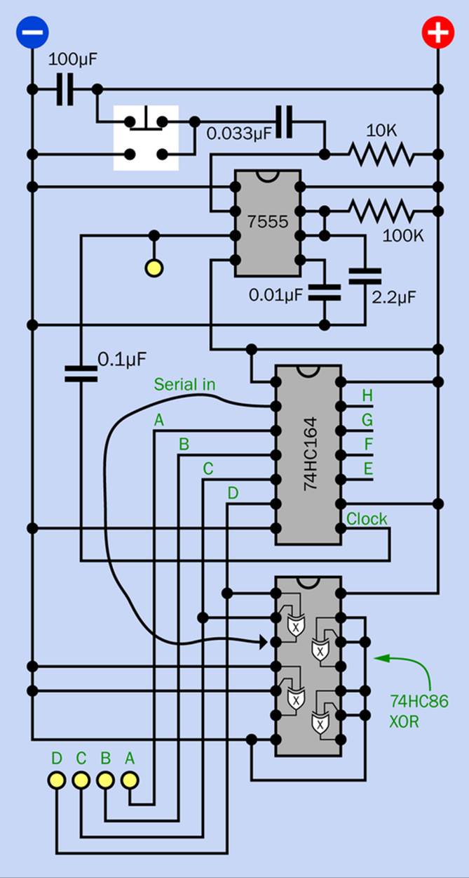
Figure 35-1. The simplest possible circuit to demonstrate a linear-feedback shift register. Negative ground connections for LEDs are not shown, and a series resistor for each LED must be added if the LEDs do not contain their own resistors.
A photograph of the breadboarded circuit appears in Figure 35-2.
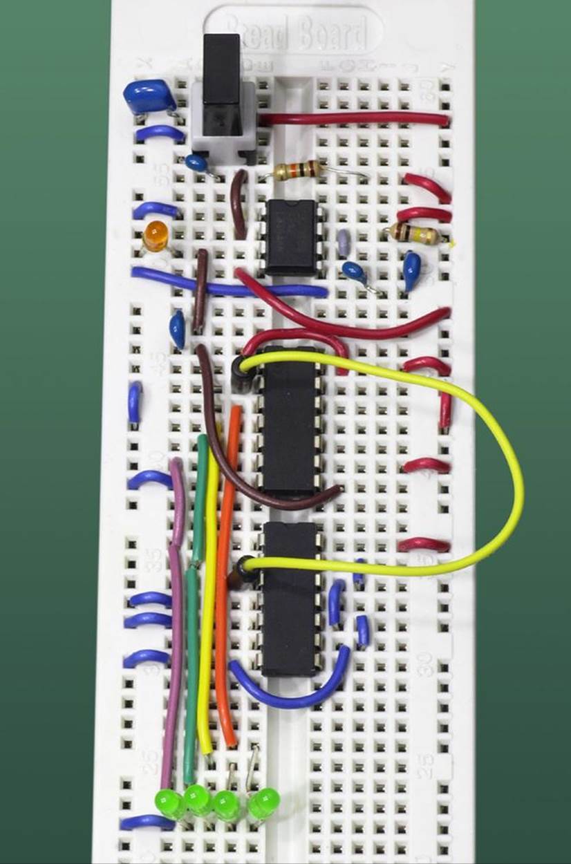
Figure 35-2. Testing the linear-feedback shift register.
Instead of a manual data input, we now have an XOR gate that taps into the outputs from the C and D memory locations and feeds them back to the serial data input. I’ve shown this connection as a wavy line, indicating a flexible jumper wire—the type with a plug on each end. Initially, both ends of this jumper are connected.
The states of the C and D memory locations recirculate. The only problem is, if you apply power cleanly to the shift register, its memory locations will all have low states. Also, when the XOR gate has two low inputs, its output will be low, too. Consequently, the feedback won’t do anything. The low states will circle around and around, and the LEDs will remain dark.
Often when you apply power to a circuit, there is an initial surge or some noise in the supply that can result in some random values being loaded into the shift register. The 100µF capacitor in the schematic is intended to stop this from happening, although it may not be entirely effective.
If you do get some initial random values, some of the LEDs will be illuminated.
Regardless of whether this happens or doesn’t happen, I want to load the shift register entirely with high states. To do this, remove the bottom end of the jumper wire from the XOR chip and apply it to the positive bus so that the serial input to the shift register will be high. Now hit the pushbutton four times to load the memory locations A, B, C, and D.
When all four LEDs are lit, reconnect the jumper to pin 3 of the XOR chip. Now press the button sixteen times, and you’ll see a sequence that should be the same as shown in Figure 35-3. It will repeat after fifteen steps, and if you changed the timer from one-shot to astable mode, the sequence would be self-sustaining.
Quick Facts About a LFSR
Summarizing what you just learned:
§ If the LEDs display low states corresponding with 0000 binary, they will remain stuck in that state, as the LFSR merely recirculates zeroes.
§ If the LEDs display any value other than 0000, they should cycle through fifteen distinct patterns before the sequence repeats. All values from 0001 through 1111 will appear, but not in numerical order. No value will be omitted (except 0000), and no value will be repeated until the whole sequence repeats.
The snag is that this sequence is so brief, your human eye and brain will soon recognize that it’s repeating.
Perhaps if we use all eight memory locations in the shift register, and increase the number of LEDs from four to eight, we will have a greater variety of patterns, and repetition will take longer to occur. This seems plausible, but before I try that, I want to show exactly what is happening here.
Bit-Shifting in Closeup
In Figure 35-3, the red boxes at the top represent memory locations in the shift register. The shifting in this figure is going to occur from right to left, as you can tell by the identifying letters A, B, C, and D. If you explore this topic elsewhere, you may find bits being shown moving from left to right, but I don’t want to do this, because I’m going to be using the shift-register outputs to represent a binary number. Moving bits from right to left makes better intuitive sense for this purpose.
Remember how a shift register works. The data input is stored in an input buffer until a clock pulse moves everything along to make room. So, when we XOR the current states of locations C and D and feed them back to the input, they stay in the input buffer until the next clock signal clocks them in. At that point, the XOR of the two new states in C and D are copied into the input buffer, until the next clock cycle—and so on.
If the memory locations are assigned the usual binary place values of 8, 4, 2, and 1 (reading from left to right), their initial decimal value will be 8 + 4 + 2 + 1 = 15. But feedback from the XOR gate will change the rightmost bit to 0, because the XOR is receiving two high inputs, which always makes it produce a low output. So on the second line, the memory locations add up to 8 + 4 + 2 = 14. On each line in the figure, the total decimal value of the binary digits is shown as black numerals in a white box.
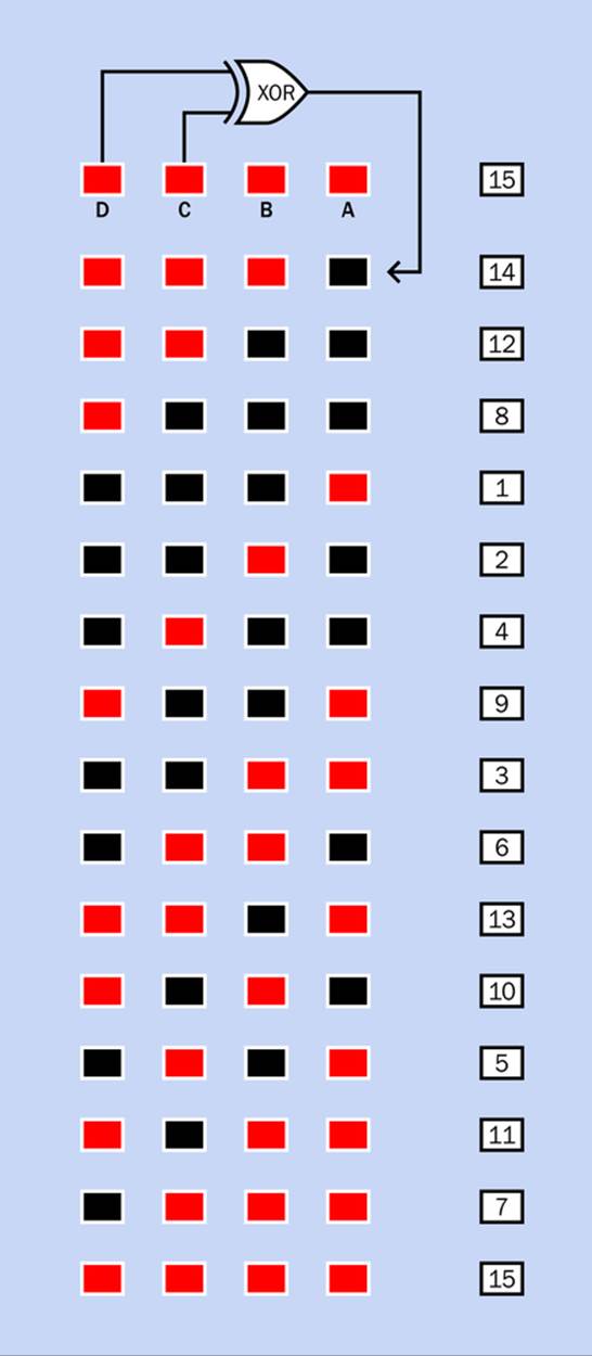
Figure 35-3. The behavior of a four-bit linear shift register.
The Problem with Zeroes
To deal with the problem of the LFSR seeming unresponsive when it is powered up with all low values in its memory locations, a text book will typically suggest preloading it with other values. This can be done with components that will run the clock of the shift register briefly while holding its data input high. But I’d like to avoid this requirement.
There’s an easier answer: rewire the circuit with an XNOR gate instead of an XOR gate. XNORs are not often used, but you can still find them in either the 74HC00 series or the 4000B series. (Another option would be to invert the output from the XOR gate, but this of course would require an inverter as an additional logic gate.)
Back in Figure 15-5, in Experiment 15, I showed that the output from an XNOR gate is the inverse of the output from an XOR gate. It responds to two low inputs by delivering a high input—so it will work in the linear feedback shift register, even if the shift register starts from 0000.
The sequence using an XNOR gate instead of an XOR gate is shown in Figure 35-4. This includes every value from 0000 through 1110 binary (0 through 14 decimal). With a little thought, you can see that 1111 will lock up the circuit with an XNOR in it, just as 0000 locks up the circuit with an XOR in it. The XNOR gate simply leaves out 1111 instead of 0000. Still, it will perform the task of starting automatically when power is first applied.
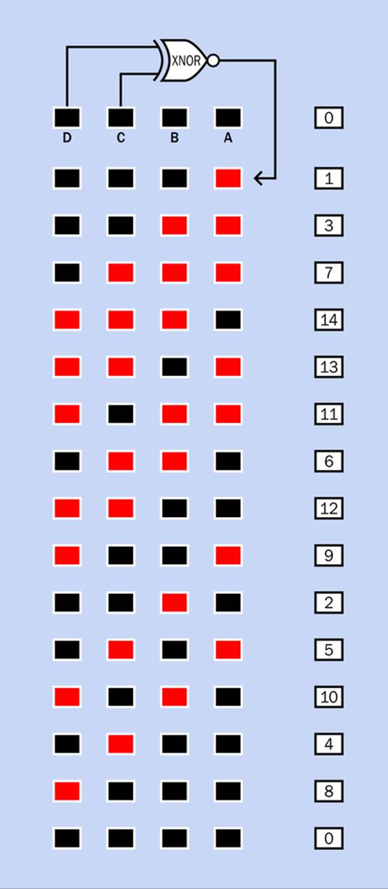
Figure 35-4. The linear-feedback shift register sequence when an XNOR gate is used to process a four-bit value beginning with 0000.
The Need to Be Nonrepeating
Before you rebuild the test circuit with a quad two-input XNOR chip, I need to get back to the issue of repetition. We really need more than fifteen steps before the sequence repeats.
Well, if we use all eight memory locations, the output values can range from 00000000 through 11111110 binary (0 to 254 decimal), and they will take 255 steps before they repeat.
This sounds more promising, but where should we put the XNOR to provide the feedback to make this happen? Will it work if we just tap into locations G and H and feed back to the input buffer?
No, if you try this, you’ll find that it does not work. Now that we are shifting eight bits, we need three XNORs, as shown in Figure 35-5. (The locations of gates would be the same if they were XORs instead of XNORs. The only difference would be that the shift register could not start containing all zeroes.)
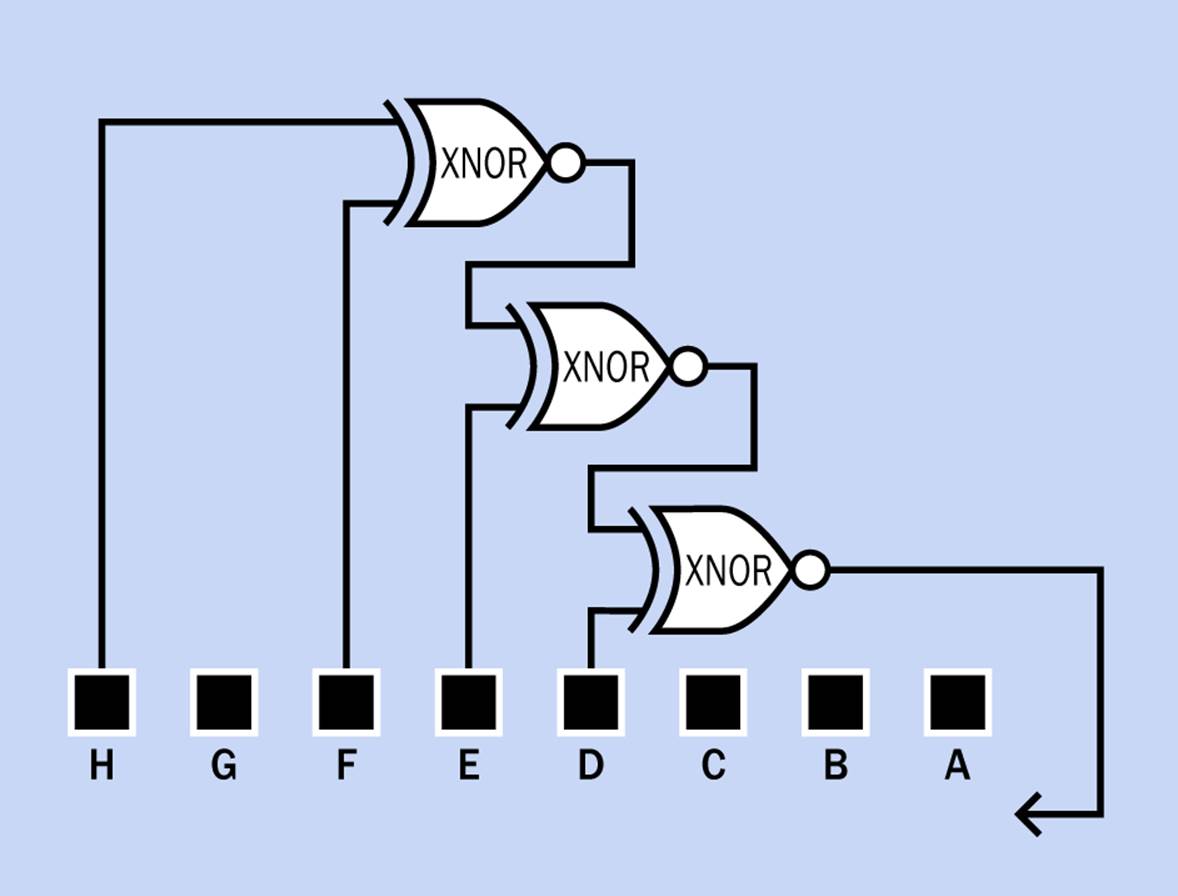
Figure 35-5. Three XNOR gates are required to make an eight-bit linear-feedback shift register.
Why do we now need three XNOR gates, and why are they in those particular locations?
Well, if we had fewer of them, or more of them, or if they were in different locations, the circuit probably would not generate a sequence including every value from 0 through 254, with no omissions and no repeats.
But how do I know this?
It can be proved mathematically. This proof is not very simple, though. It gets us into areas such as “primitive polynomials” and “finite field arithmetic” that are difficult to understand and would require many pages to explain—even if I were qualified to explain them.
If I can’t prove it to you, how can you be sure it’s right?
The answer is, we can test the theory by making an observation. Figure 35-6 shows the linear feedback circuit that replicates the logic in Figure 35-5. You can trace this out very easily.
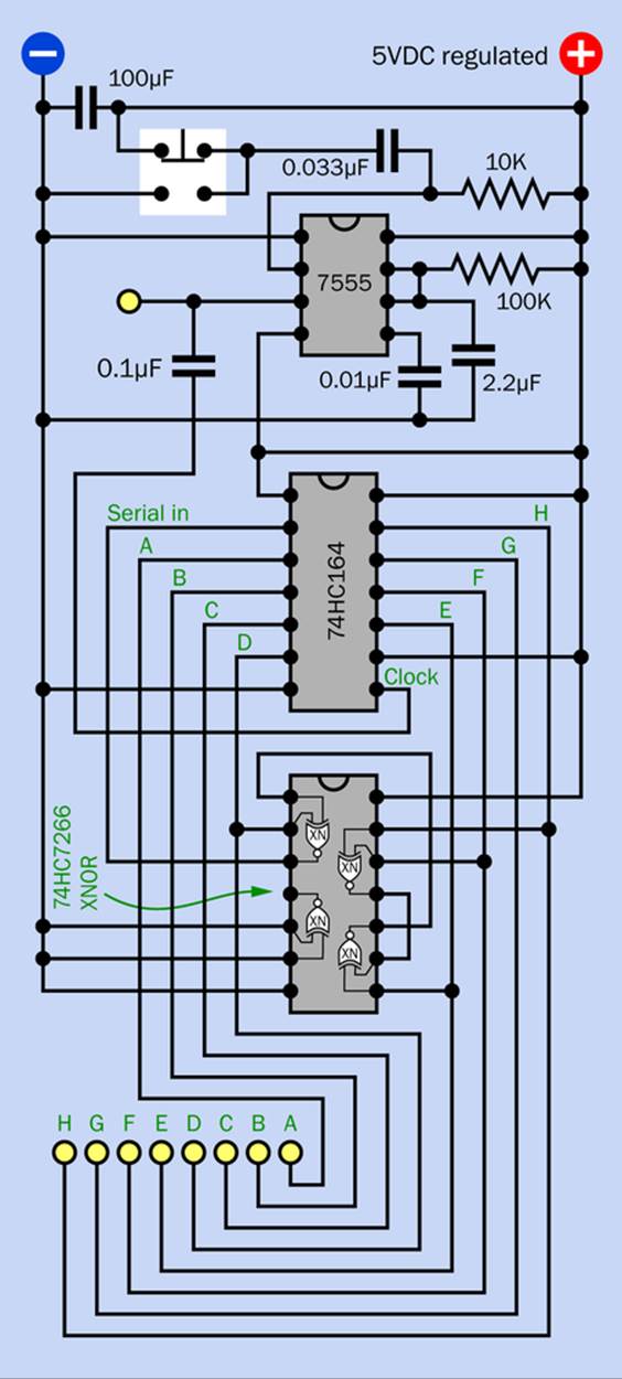
Figure 35-6. Schematic for an 8-bit linear feedback shift register test. Negative ground connections for LEDs are not shown, and a series resistor for each LED must be added if the LEDs do not contain their own resistors.
Shift register outputs H and F are tapped to provide inputs to the top-right XNOR gate in the XNOR chip. The output from that gate goes to an input on the gate below it, which also receives and input from output E. The XNORed output from that gate goes around to the top left gate, which receives an input from output D. The XNORed output from that gate feeds back to the serial input of the shift register.
At the top of the circuit there is a debounced pushbutton so that you can step through the sequence at your leisure.
The breadboarded version of the circuit is shown in Figure 35-7.
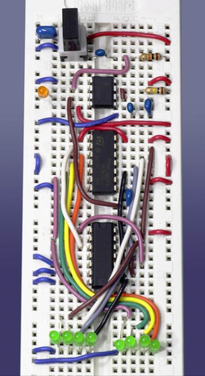
Figure 35-7. The 8-bit linear-feedback shift register, breadboarded.
Warning: XNOR Idiosyncracies
Make sure you wire the XNOR chip correctly. Its internal connections are totally different from those of all other logic chips. Just for the record, the pinouts are shown in Figure 35-8. If you make the mistake of wiring it like an OR gate or an XOR gate, you may damage it permanently.
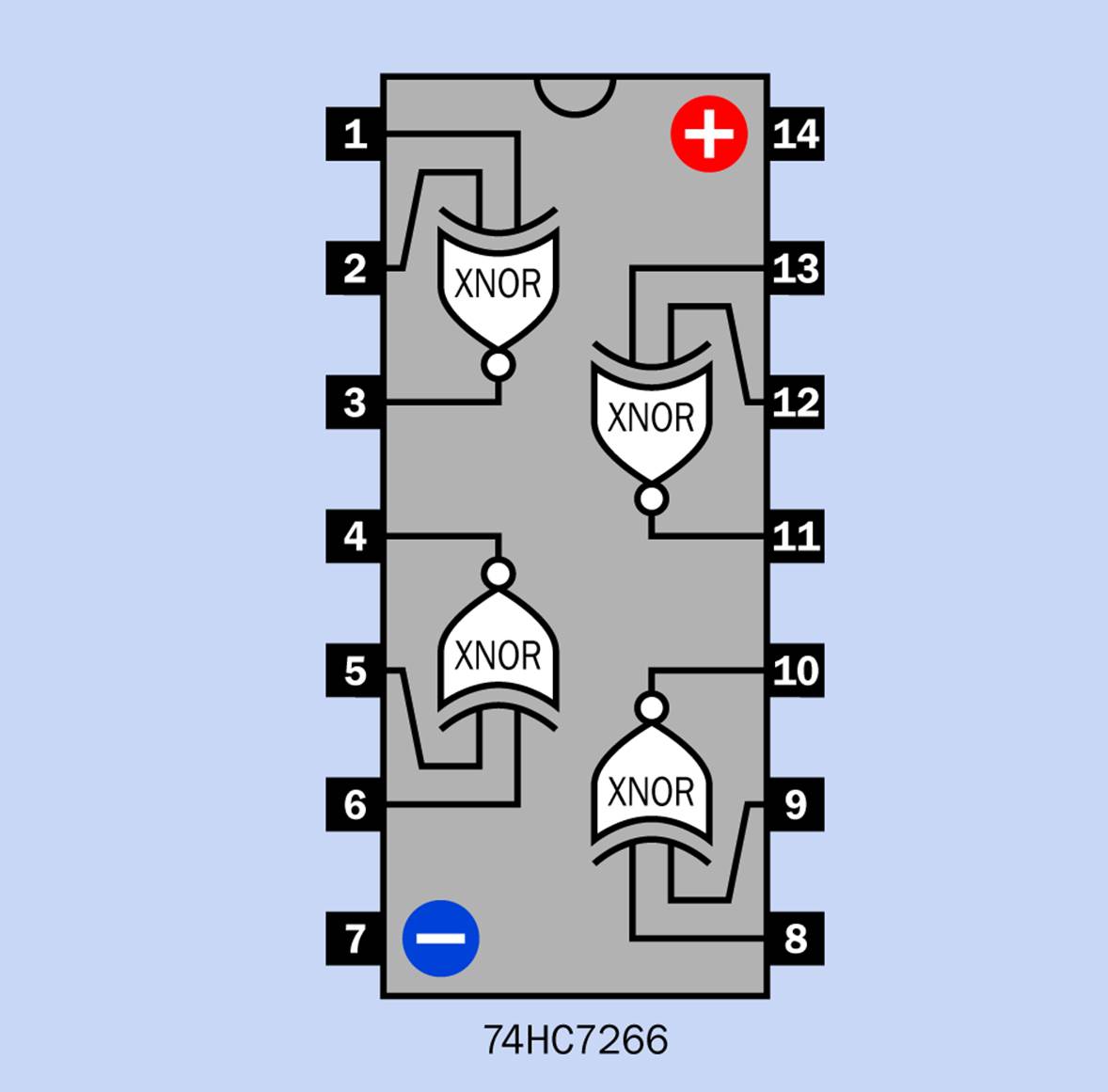
Figure 35-8. Pinouts of a quad two-input XNOR chip. The internal connections of this chip are different from those of all other chips containing logic gates.
Another thing to watch out for is that there is a variant of the XNOR chip under the part number 74HC266, which is just one digit different from the 74HC7266. The 74HC266 version of the XNOR chip has open-drain outputs, which are intended to control loads of up to 100mA and must not be connected with other chips. The Texas Instruments SN74HC266N is an example. Don’t buy it by mistake!
The 74HC7266 is what you want, but it costs a bit more than most logic chips. You can alternatively use the 4077 (the old CMOS version) which is one-quarter the price. The pinouts are exactly the same.
Running the Test
Because I want your results from this test to be exactly the same as my results, you need to start with your shift register in the same state that I used with mine. I made sure that it had a low state in every memory location. If you don’t see this when you power up, you’ll have to take care of it manually, as you did in the four-bit LFSR test.
Follow these steps carefully:
1. Unplug the lower end of the jumper that normally connects with the output from the top-left XNOR gate. This is the “Serial In” jumper. Leave the top end connected.
2. Plug the lower end of the jumper into the negative bus.
3. Hit the pushbutton eight times to clock in eight zeroes.
4. Veeery carefully reattach the lower end of the jumper to the output from the XNOR gate.
Now when you start using the LFSR, the sequence you get will match the sequence that I am about to show you.
This sequence is listed in Figure 35-9, where 0 represents an LED that is off and 1 represents an LED that is on. Each time you press the button, the next line in the figure should match the LEDs on your breadboard.
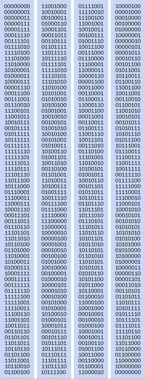
Figure 35-9. The sequence of 255 outputs from an 8-bit linear feedback shift register, plus a repeat of the initial state.
You may be wondering how I generated the listing. Did I laboriously type it with one hand, while pressing the debounced pushbutton with the other? Well, actually, no. I wrote a little computer program that emulated a linear-feedback shift register, and I saved the output. However, I did check the output against the performance of the actual circuit—and now, so can you.
Binary numbers are difficult for the human brain to interpret, so I also generated the same sequence in decimal values. Here it is:
0, 1, 3, 7, 15, 30, 61, 122, 244, 232, 208, 161, 67, 135, 14, 28, 57, 114, 229, 203, 151, 47, 95, 191, 127, 254, 253, 251, 247, 238, 220, 184, 113, 227, 199, 142, 29, 59, 118, 237, 218, 180, 104, 209, 163, 71, 143, 31, 63, 126, 252, 249, 243, 230, 205, 155, 54, 109, 219, 182, 108, 217, 178, 100, 200, 145, 35, 70, 141, 27, 55, 111, 223, 190, 125, 250, 245, 234, 212, 169, 82, 164, 73, 146, 37, 74, 148, 41, 83, 166, 77, 154, 52, 105, 211, 167, 79, 158, 60, 120, 240, 224, 193, 130, 4, 9, 18, 36, 72, 144, 33, 66, 133, 10, 20, 40, 81, 162, 69, 139, 23, 46, 93, 187, 119, 239, 222, 188, 121, 242, 228, 201, 147, 39, 78, 156, 56, 112, 225, 195, 134, 12, 24, 49, 99, 198, 140, 25, 51, 103, 206, 157, 58, 116, 233, 210, 165, 75, 150, 45, 91, 183, 110, 221, 186, 117, 235, 214, 173, 90, 181, 106, 213, 171, 86, 172, 88, 177, 98, 196, 136, 17, 34, 68, 137, 19, 38, 76, 152, 48, 97, 194, 132, 8, 16, 32, 64, 129, 2, 5, 11, 22, 44, 89, 179, 102, 204, 153, 50, 101, 202, 149, 43, 87, 174, 92, 185, 115, 231, 207, 159, 62, 124, 248, 241, 226, 197, 138, 21, 42, 85, 170, 84, 168, 80, 160, 65, 131, 6, 13, 26, 53, 107, 215, 175, 94, 189, 123, 246, 236, 216, 176, 96, 192, 128, 0
To me, that looks satisfactorily pseudorandom. My program also checked to make sure that each value is included once, and only once, without any omissions or repetitions.
Ones and Zeroes
Having verified that the logic diagram in Figure 35-5 really will work as advertised, the next step is to decide how we reduce this sequence so that it generates just a single 1 or 0 in each cycle. Remember, we want to use this for the Telepathy Test, where the circuit will switch on an LED, or switch it off.
One way would be XORing the outputs from the shift register, just as I did with the outputs of the rotational encoders in Experiment 33. That would work, and you could use a “tree” of three levels of XOR gates, each averaging the outputs of the previous layer, to get down to a 0 or 1 output.
However, this isn’t necessary. All we need to do is tap into the “A” memory location of the shift register, and use that.
At first this makes no sense. We included more outputs from the shift register to get a sequence that runs through more states before it repeats. And now we’re just going to throw away those extra digits?
Not quite. All eight memory locations are still being used in the feedback process. The eighth, sixth, fifth, and fourth locations will still be XNORed as before, so we will still have a sequence that runs through 255 states before it repeats. I’m just suggesting we can subsample it.
The entire pattern of ones and zeroes will still take 255 steps before it repeats.
Perhaps you find this hard to believe. In fact, I wasn’t totally convinced of it myself. Theory told me that it should be true, but I decided to confirm it with another observation. I modified my computer program to sample only the rightmost digit from each of the 255 steps in the linear feedback process, and got this sequence of 1s and 0s:
01111010000111001011111110111000 11101101000111111001101101100100 01101111101010010010100110100111 10000010010000101000101110111100 10011100001100011001110100101101 1101011010101100010001001100001000000101100110010101110011111000 1010101000001101011110110000000
Then I ran the actual circuit, looking only at the rightmost LED. I got exactly the same series. When you predict something like this, and it turns out to be precisely correct, that provides excellent evidence that it should happen every time.
You may object that this sequence doesn’t seem entirely random, because it has patterns such as 0000000 and 1111111 in it. Yes, indeed it does, but a random sequence actually should contain some repetitions of this type. Remember, when you toss a coin, it can come up heads or tails several times in succession. In fact, the probability of multi-digit repetitions increases as the number of trials increases.
So, the presence of some repeated numbers in the sequence above is not a matter for concern. Of course, if the sequence consisted mostly of 11111111 and 00000000 combinations, that would be a different matter; but the distribution of patterns is actually very good. I counted the frequency of repeated sequences of 1s and 0s, and they look like this:
0 alone — 33 times
00 — 16 times
000 — 8 times
0000 — 4 times
00000 — 2 times
000000 — 1 time
0000000 — 1 time
Total: 128 instances of value 0.
1 alone — 32 times
11 — 16 times
111 — 8 times
1111 — 4 times
11111 — 2 times
111111 — 1 time
1111111 — 1 time
Total: 127 instances of value 1.
The Problem of Weighting
There’s only one thing that doesn’t look quite right in the list that I just presented. There are 33 single zeroes, but 32 single ones. What? This sequence was supposed to be absolutely evenly weighted!
No, I said it would be absolutely evenly weighted, “almost.”
Here’s the problem (which will then lead us to a solution). The entire sequence of all possible values would be 00000000 through 11111111 before it repeats. But you’ll recall that using XNOR gates for feedback, the XNOR-based shift register is unable to display 11111111, so it skips it. Because that value has a 1 at the end, there is a 1 missing from our tabulation of digits at the end of each number.
Suppose I try to get around the problem by using the penultimate digit instead of the last digit. No, that won’t solve the problem, because 11111111 is still missing, so there will be one more 0 than 1 in the final tabulation.
I will address this issue.
Skipping 254
One answer would be to add more shift registers. Suppose I have four of them chained together, providing enough memory locations to store a binary sequence of thirty-two digits. A complete sequence from this LFSR will run through more than four trillion values before it repeats. In that sequence, every pattern of thirty-two ones and zeroes will be represented except for the last, consisting of thirty-two ones. That missing single value will now be buried among more than four trillion others—which I think should be acceptable for just about any purpose.
Unfortunately, building that circuit would entail more work. Do you want to wire four shift registers and an unknown number of XNORs to create the linear feedback, plus additional components, to make the output from the Telepathy Test more perfectly balanced? If you do, that’s great! I’d love to see someone do this! Personally, however, I don’t have time, because—well, I already told you, I have to finish writing this book, to give you an opportunity to read it.
So how about an easier alternative? We can simply tell the shift register (somehow) to skip an eight-bit pattern that would have created a 0 as the last bit, to make up for the missing 11111111 that has a 1 as the last bit. Then the outputs will be even.
Since 11111111 is already missing, we could get rid of 11111110 as well (254, in decimal notation). That will be easy: just use a seven-input AND gate to look for 1111111 in places B through H, and when its output goes positive, use it to advance the clock to the next value. The complete logic diagram is shown in Figure 35-10.
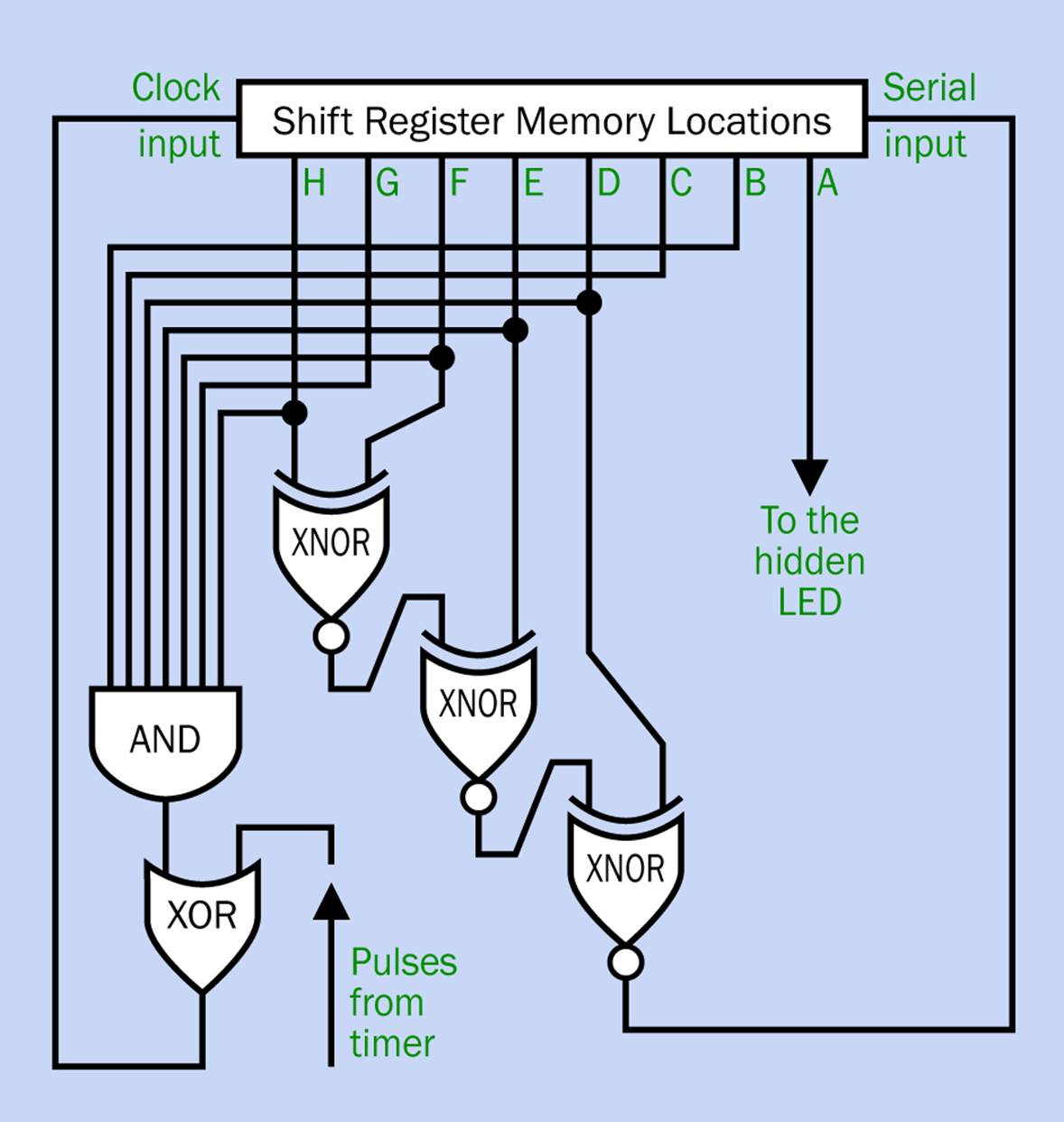
Figure 35-10. Logic diagram for a linear feedback shift register with an evenly weighted binary output, achieved by forcing the register to skip the state 11111110.
Is there such a thing as a seven-input AND gate? No, but you can buy one with eight inputs. If the eighth input is tied to the positive side of the power supply, the remaining seven can be ANDed. This chip is in the old 4000B series, not the 74HC00 series, but it will work.
Sharing the Clock Input
You’ll notice that the seven-input AND does not feed back directly to the clock input of the shift register. That’s because the clock input must also be used by a timer (or other input) that advances the shift register on a regular basis. I’ll call this the “regular clock” to distinguish it from the “AND input.”
To deal with the situation, I have added an XOR gate. Here is the imaginary sequence of events:
1. The XNOR feedback has reached the value 11111110, which we want to skip. It is applied to the input buffer.
2. The regular clock moves the 11111110 forbidden state into the shift register.
3. The eight-input AND gate immediately detects this and emits a high output. This feeds into the XOR gate.
4. The regular clock pulse hasn’t ended yet, so the XOR gate has two high inputs. It switches to a low output.
5. The regular clock pulse ends. But the 11111110 forbidden state is still generating a high output from the AND gate.
6. The XOR now has one high input from the AND gate, and a low input from the regular clock. So the XOR output goes high.
7. The high XOR output triggers the shift register to move on to the next combination.
8. The AND gate doesn’t sense the 11111110 forbidden state anymore, so its output goes low.
9. The shift register is now stable until the next regular clock pulse comes along.
You see from the above, there will be a moment while the forbidden 11111110 state is active, but only for the remainder of a clock pulse. If the pulse is very brief, the 11111110 state will be skipped almost immediately. During the Telepathy Test, it the state won’t last long enough to light the LED.
At least, I think this is how it will work. In the next experiment, we’ll confirm that it works.
Any Other Options?
Blocking one input pattern is not a very elegant solution to the problem. Maybe there’s a better way, but if there is, I’m not sure what it is. I even consulted some friends in the encryption business, where big LFSRs generate pseudorandom numbers, but they just told me to use more shift registers—which I had already decided would be too much trouble.
So, my solution to the problem has to be skipping an input, for better or worse.
Seeding
One thing that still has to be taken care of is that so long as there are no voltage spikes, we will always start with a value of 00000000 in the shift register.
Obviously if we want to make a game seem unpredictable, it won’t achieve its goal if it starts in exactly the same way every time. We must start at an unknown point in the sequence. How can we deal with this?
The answer is very simple. It is standard practice to “seed” a random-number generator with a value that will not be the same every time. In a computer program, often the system clock in the computer is used for this purpose, because the time represented by the clock is constantly changing. In the XNOR Randomizer, ideally you should run it for an arbitrary number of cycles before you use its output in a game.
Well—no problem! We can use the system I mentioned in Experiment 34, where a resistor-capacitor combination triggers a single-pulse, slow-running timer when power is switched on. The duration of this timer pulse will be adjusted by a sensor of some type. During the pulse, the slow timer allows a fast asynchronous timer to run. The asynchronous timer cycles the clock input of the LFSR. At the end of the pulse from the slow timer, the LFSR stops in an unknown state, and we’re ready for some perfectly balanced pseudorandomicity.
Make Even More: Other Games and Other Numbers
Before I get to the Telepathy Test, I want to show you how many ways there are to use the output from an LFSR. I’m going to call it an All-Purpose 8-Bit Randomizer, with applications such as the ones below.
Twinkling LEDs
Suppose you have eight LEDs: two red, two green, two blue, and two yellow. Each pair of LEDs is powered by two outputs from a linear-feedback shift register. One output goes through a 330Ω resistor, while the other goes through a 1K resistor. Each color will now have four states: off, low, medium, and high intensity. Figure 35-11 shows how this could be done, using a Darlington array so that you can have bright, high-current LEDs.
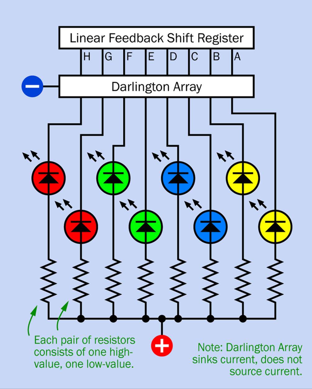
Figure 35-11. Using the linear-feedback shift register to create pseudorandom twinkling LEDs.
If you mount the LEDs behind a diffusing panel (like the plastic diffusers that are used with recessed fluorescent tubes), you’ll get an attractive twinkling effect when the shift register is running at a fairly high clock speed.
Slot selector
The linear-feedback shift register can run the multiplexer in the Hot Slot game. Just connect four of the register outputs to the multiplexer control lines.
Ring counter variant
In Experiment 26, a ring counter flashed sixteen LEDs sequentially. We could use an LFSR to flash them randomly, powering them through a multiplexer. If there are also sixteen buttons, one beside each LED, the challenge will be to press a button while the LED beside it is still illuminated.
The same voltage that powers the LED can be applied to the contacts in the pushbutton, and the other sides of the pushbuttons will connect with a beeper, so that if you press the button while the LED is on, you’ll hear a beep and your score will increment. SeeFigure 35-12.
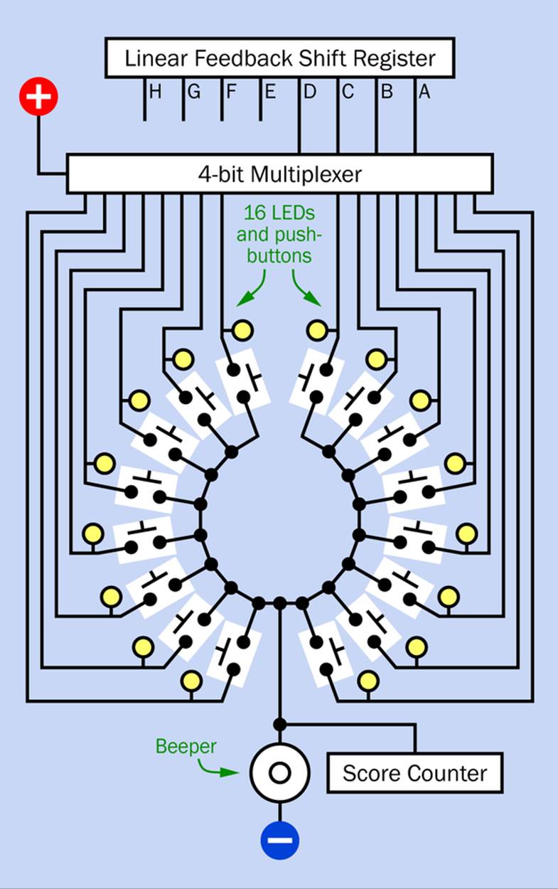
Figure 35-12. The game in Experiment 26, using a ring counter, could be remade with a linear feedback shift register to flash LEDs randomly. The player tries to press the button beside each LED while it is illuminated.
If you use reed switches instead of pushbuttons, you could put everything, including the LEDs, behind a thin membrane of translucent plastic. A reed switch would be hidden beside each LED. The player would point to the LED with a magnet-tipped stylus, thus activating the reed switch beside it. This would be an elegant user interface, and it would eliminate the problem of a player cheating by touching multiple switches. Of course, you would have to choose the strength of the magnet carefully so that it would activate one reed switch reliably without affecting the other switches either side.
Random tones
Still using four outputs to control a multiplexer, it could connect one of sixteen resistors to a timer running at audible frequencies. If you use trimmer potentiometers instead of fixed-value resistors, you can tune each of them to produce a note in the diatonic scale. (You would need a keyboard instrument for reference to get the tuning right.)
The result would not be music, as such, but if the pitch changes occurred slowly, they could be interesting. See Figure 35-13.
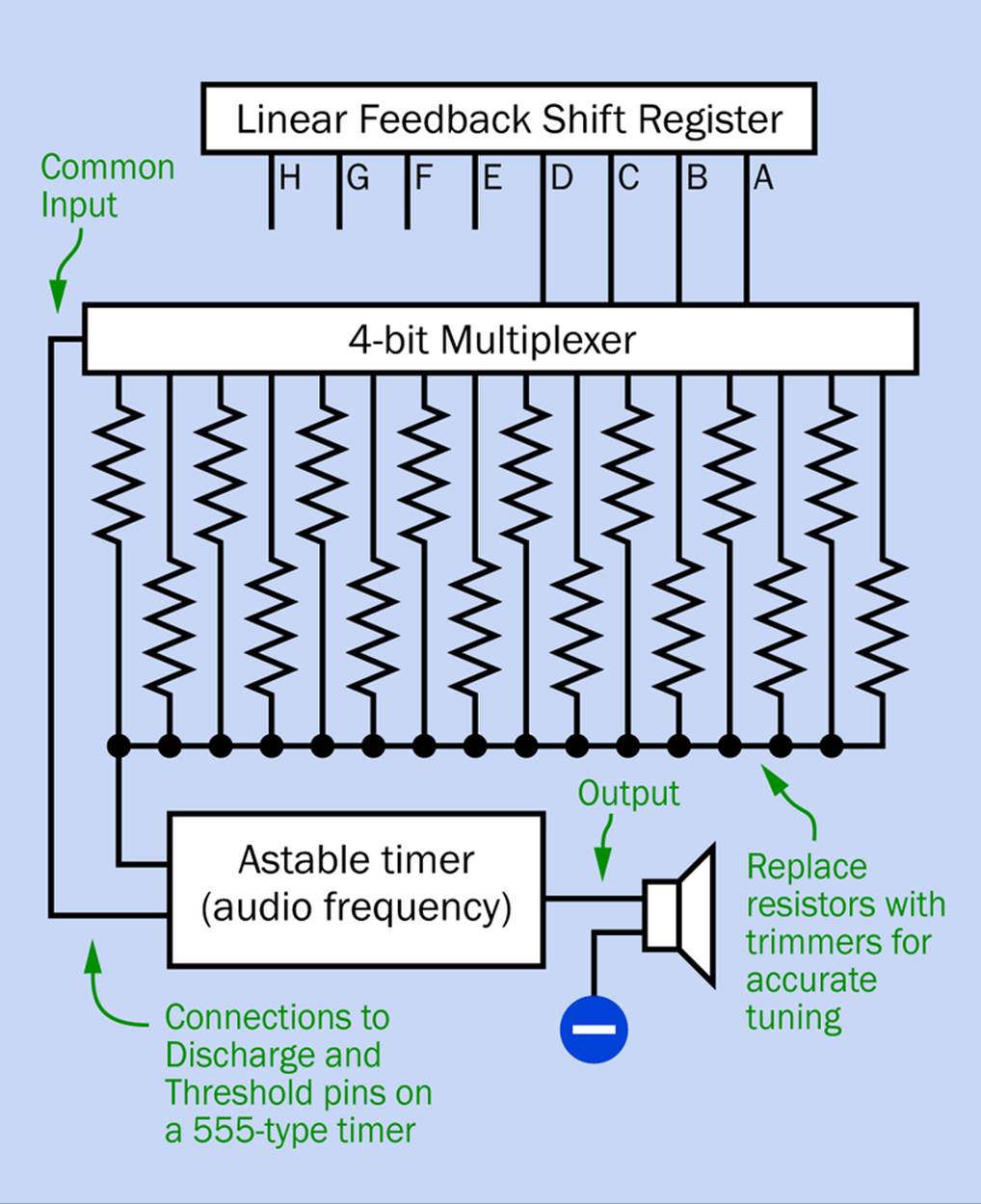
Figure 35-13. Using an LFSR to create sixteen random musical tones.
An alternative would be to use two multiplexers, each using four of the eight outputs from the shift register. One multiplexer would control pitch, while the other could set sound quality by inserting resistor-capacitor combinations between the output and negative ground. See Figure 35-14.
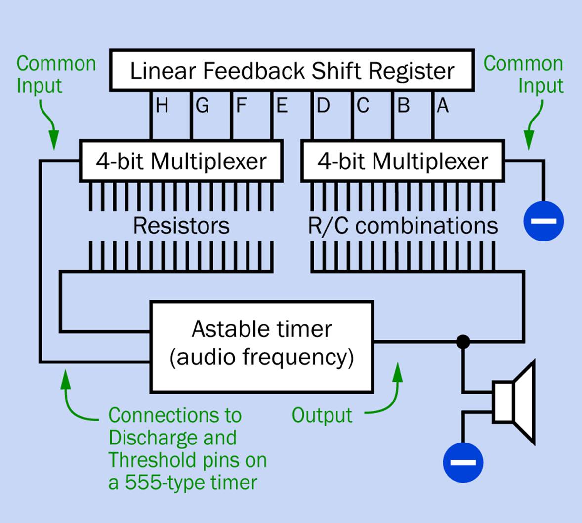
Figure 35-14. Resistor-capacitor combinations could be selected randomly by a second multiplexer to add tonal variety to a random-tone generator.
Ching input
Instead of the fingertip-resistance randomizer that I suggested for the Ching Thing (see Chapter 27) you could use four outputs from the linear-feedback shift register to control the decoder chip.
Make Even More: Microcontroller Randomicity
The concept of a linear feedback shift register is used in computer languages to create pseudo-random number sequences. This includes the high-level languages that are installed in some microcontrollers. Depending which microcontroller you are using, some sort of statement should allow your program to generate a seemingly random number on demand.
But will the distribution of values be evenly weighted? I have to say that when I investigated the random number function in the version of BASIC implemented on a PIC microcontroller (the so-called PICAXE), I was not impressed. Depending on the range that I specified, some values came up significantly more often than others.
If you’re wondering if C language on the Arduino is more likely to give you a better simulation of randomicity, I encourage you to test it to find out. Note that it is common practice to read the value of an unconnected pin on the chip, via the internal analog-to-decimal converter, to start the internal random-number generator with an unpredictable value.
All materials on the site are licensed Creative Commons Attribution-Sharealike 3.0 Unported CC BY-SA 3.0 & GNU Free Documentation License (GFDL)
If you are the copyright holder of any material contained on our site and intend to remove it, please contact our site administrator for approval.
© 2016-2026 All site design rights belong to S.Y.A.