PIC32 Microcontrollers and the Digilent chipKIT: Introductory to Advanced Projects (2015)
Chapter 2. PIC32 Microcontroller Series
Abstract
This chapter is an introduction to the hardware of the PIC32 family of microcontrollers. The architecture of the popular PIC32MX360F512L microcontroller is taken as an example in this chapter. The program and data memory structure, reset circuitry, clock sources, I/O port characteristics, real-time clock module, and various timer modules offered by the chip are described in detail. In addition, the important topic of interrupts is covered and the interrupt mechanisms and interrupt sources of the PIC32 family of microcontrollers are described. Finally, the analogue input structure and the ADC module of the PIC32MX360F512L microcontroller are given with examples to show how this microcontroller can be used in analogue input applications.
Keywords
32-Bit microcontrollers
Architecture of the PIC32 family
Program memory
Data memory
The power supply
Reset mechanisms
Clock modules
I/O ports
Timer modules
Interrupts
Priorities
ADC converter
PIC32 is a 32-bit family of general-purpose, high-performance microcontrollers manufactured by Microchip Technology Inc. Looking at the PIC microcontroller development history, based on their performance, we can divide the PIC microcontroller families into low-performance, low-to-medium–performance, medium-performance, and high-performance devices.
Low-performance PIC microcontrollers consist of the basic 8-bit PIC10 and PIC16 series of devices that have been around for over a decade. These devices are excellent general-purpose low-speed microcontrollers that have been used successfully in thousands of applications worldwide.
The PIC18 series of microcontrollers were then introduced by Microchip Technology Inc. as low-to-medium–performance devices for use in high–pin count, high-density, complex applications requiring large number of I/O ports, large program and data memories, and supporting complex communication protocols such as CAN, USB, TCP/IP, or ZigBee. Although these devices are also based on 8-bit architecture, they offer higher speeds, from DC to 40 MHz, with a performance rating of up to 10 MIPS.
The PIC24 series of microcontrollers are based on 16-bit architecture and have been introduced as medium-performance devices to be used in applications requiring high compatibility with lower-performance PIC microcontroller families, and at the same time offering higher throughput and complex instruction sets. These microcontrollers have been used in many real-time applications such as digital signal processing, automatic control, speech and image processing, and so on, where higher accuracy than 8 bits is required, and at the same time higher speed is the main requirement.
PIC32 microcontroller family has been developed for high-performance, general-purpose microcontroller applications. The family offers 80 MIPS performance with a wide range of on-chip peripherals, large data and program memories, large number of I/O ports, and an architecture designed for high-speed real-time applications. PIC32 microcontrollers can be used in real-time applications requiring high throughput. Some of the application areas are digital signal processing, digital automatic control, real-time games, and fast communication. The chip employs the industry standard M4K MIPS32 core from MIPS Technologies Inc. PIC32 family offers programming interface similar to other PIC microcontroller families, thus making the programming an easy task if the programmer is already familiar with the basic PIC microcontroller architecture. PIC32 microcontrollers are pin-to-pin compatible with most members of the PIC24 family of 16-bit microcontrollers; thus, the migration from 16- to 32-bit operation should be relatively easy.
Figure 2.1 shows a simplified architectural overview of the PIC32 microcontrollers. At the heart of the microcontroller is a 32-bit M4K MIPS32 core processor that connects to the rest of the chip via a bus matrix and a peripheral bus. The bus matrix runs at the same speed as the core processor and connects various high-speed modules such as the USB, DMA, memory, ports, and so on. The peripheral bus can be programmed to run at slower speeds, and it connects to slower modules such as A/D converter, UART, SPI, Real-Time Clock and Calendar (RTCC), and so on.
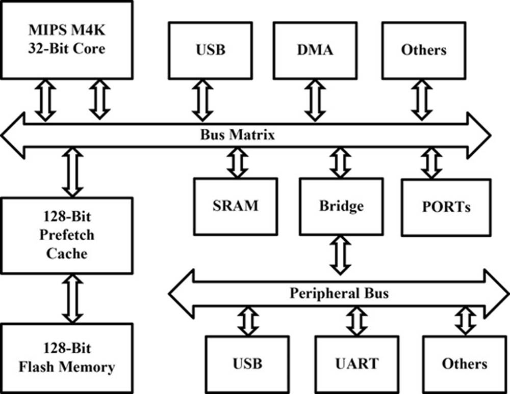
FIGURE 2.1 Simplified Architecture of the PIC32 Microcontroller Family
The core processor has the following features:
• 80 MHz clock speed
• 32-Bit address bus and 32-bit data bus
• Five-stage pipelining
• Single-cycle ALU
• Single-cycle multiply and high-speed divide module
• 2 × 32 register files
Other important features of the chip are the following:
• 2.3–3.6 V operation
• Up to 512k flash program memory
• Up to 32k SRAM data memory
• Internal oscillators
• Multiple interrupt vectors
• UART, SPI, and I2C modules
• Configurable watchdog timer and real-time clock
• High-speed I/O with 18 mA current sink/source capability
• Configurable open-drain output on I/O pins
• External interrupt pins
• PWM, capture, and compare modules
• JTAG debug interface
• Fast A/D converter and analogue comparator modules
• Timers and counters
• Hardware DMA channels
• USB support
• Large pin count for a wide range of peripherals and I/O ports
• Wide operating temperature (−40 to +105°C)
Different chips in the family may have additional features, such as Ethernet support, CAN bus support, and so on.
Perhaps the best way of learning the PIC32 microcontroller family architecture is to look at a typical processor in the family in greater detail. In this book, the Digilent Cerebot MX3cK Development Board (has been renamed to chipKIT MX3) will be used. This board is equipped with the PIC32MX320F128H microcontroller (from the PIC32MX3XX/4XX family). In this chapter, we shall be looking at the architecture of the PIC32MX360F512L microcontroller from the same family. The architectures of other members of the PIC32 microcontroller family are very similar to the chosen one and should not be too difficult to learn them.
2.1. The PIC32MX360F512L Architecture
The PIC32MX360F512L is a typical PIC32 microcontroller, belonging to the family PIC32MX3XX/4XX. This microcontroller has the following features:
• A 100-pin (TQFP) package
• Up to 80 MHz clock speed
• 512k flash program memory (+12k boot flash memory)
• 32k data memory
• 5 × 16-bit timers/counters
• 5 × capture inputs
• 5 × compare/PWM outputs
• Four programmable DMA channels
• 2 × UARTs (supporting RS232, RS485, LIN bus, and iRDA)
• 2 × SPI bus modules
• 2 × I2C bus modules
• RTCC module
• 8 MHz and 32 kHz internal clocks
• 16 × A/D channels (10 bits)
• 2 × comparator modules
• Four-wire JTAG interface
PIC32MX360F512L is available in a 100-pin TQFP package as shown in Figure 2.2. The pins that are +5 V–tolerant are shown in bold.
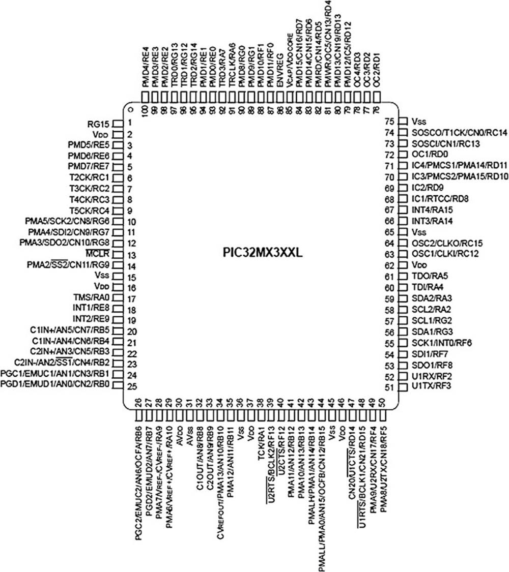
FIGURE 2.2 Pin Configuration of the PIC32MX360F512L
Figure 2.3 shows the internal block diagram of the PIC32MX360F512L microcontroller. In the middle of the diagram, we can see the MIP32 M4K processor. The 32-bit data memory is directly connected to the processor via the bus matrix, offering up to 4 GB addressing space. The 1298-bit flash program memory is also connected to the bus matrix via a 32-bit prefetch module. The 32-bit peripheral bridge connects the bus matrix and the processor to the peripheral modules. The peripheral modules consist of the following:
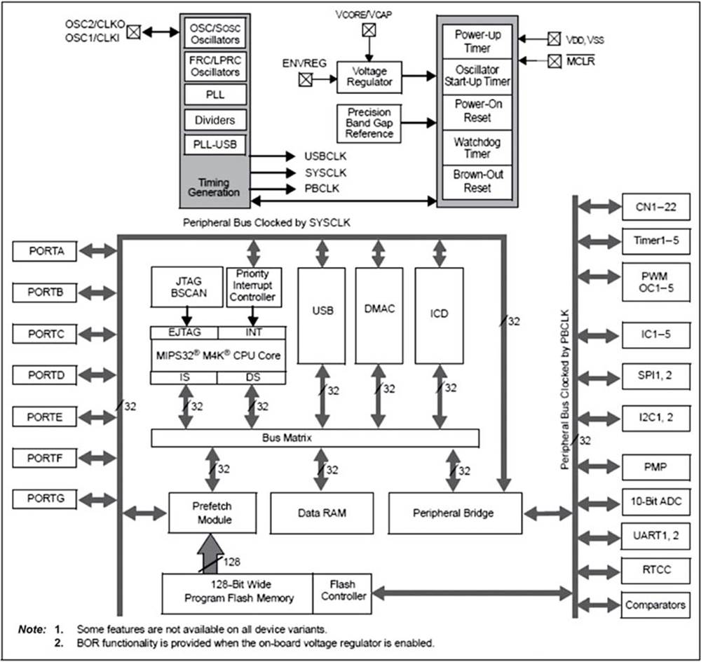
FIGURE 2.3 Block Diagram of the PIC32MX360F512L
• Seven ports (PORTA to PORTG)
• 5 × timer modules
• 5 × PWM modules
• 2 × SPI bus modules
• 2 × I2C modules
• 10-Bit ADC module
• 2 × UART modules
• RTCC module
• Comparators
• Change notification inputs
The system clock and peripheral bus clock are provided by the Timing Generation module, which consists of the following:
• Oscillators
• PLL module
• Clock dividers
The Timing Generation module additionally provides clock to the following modules:
• Power-up timer
• Oscillator start-up timer
• Power-on reset (POR)
• Watchdog timer
• Brown-out reset (BOR)
The functions of the pins are summarised in Table 2.1.
Table 2.1
Pin descriptions.
|
Pin name |
Description |
|
AN0–AN15 |
Analogue inputs |
|
CN0–CN21 |
Change notification inputs |
|
IC1–IC5 |
Capture inputs |
|
OC1–OC5 |
Output compare outputs |
|
INT0–INT4 |
External interrupt inputs |
|
RA0–RA15 |
PORTA pins |
|
RB0–RB15 |
PORTB pins |
|
RC1–RC15 |
PORTC pins |
|
RD0–RD15 |
PORTD pins |
|
RE0–RE9 |
PORTE pins |
|
RF0–RF13 |
PORTF pins |
|
RG0–RG15 |
PORTG pins |
|
T1CK–T5CK |
Timer external clock inputs |
|
U1CTS/U1RTS/U1RX/U1TX |
UART1 pins |
|
U2CTS/U2RTS/U2RX/U2TX |
UART2 pins |
|
SDI1/SDO1/SS1/SCK1 |
SPI1 pins |
|
SDI2/SDO2/SS2/SCK2 |
SPI2 pins |
|
SCL1/SDA1 |
I2C1 pins |
|
SCL2/SDA2 |
I2C2 pins |
|
TMS/TCK/TDI/TDO |
JTAG pins |
|
RTCC |
Real time clock alarm output |
|
CVREF–/CVREF+/CVREFOUT |
Comparator voltage reference pins |
|
C1IN–/C1IN+/C1OUT |
Comparator 1 input–outputs |
|
C2IN–/C2IN+/C2OUT |
Comparator 2 input–outputs |
|
PMA0–PMA15 |
Parallel Master Port address bits |
|
PMCS1/PMCS2 |
Parallel Master Port chip select pins |
|
PMD0–PMD15 |
Parallel Master Port data pins |
|
PMRD/PMWR/PMALL/PMALH |
Parallel Master Port control pins |
|
OCFA/OCFB |
Output compare fault inputs |
|
TRCLK |
Trace clock |
|
TRD0–TRD3 |
Trace data pins |
|
PGED1/PGEC1/PGED2/PGEC2 |
Programming/debugging pins |
|
MCLR |
Master Clear pin |
|
AVDD/AVSS/VREF+/VREF- |
ADC pins |
|
VDD/VSS |
Microcontroller supply pins |
|
OSC1/OSC2/CLK0/CLK1/SOSC1/SOSCO |
Oscillator input–outputs |
2.1.1. The Memory
Figure 2.4 shows the memory structure of the PIC32MX3XX/4XX microcontrollers. The memory structure may look complicated initially, but the explanation given in this section should make it simple and easy to understand.
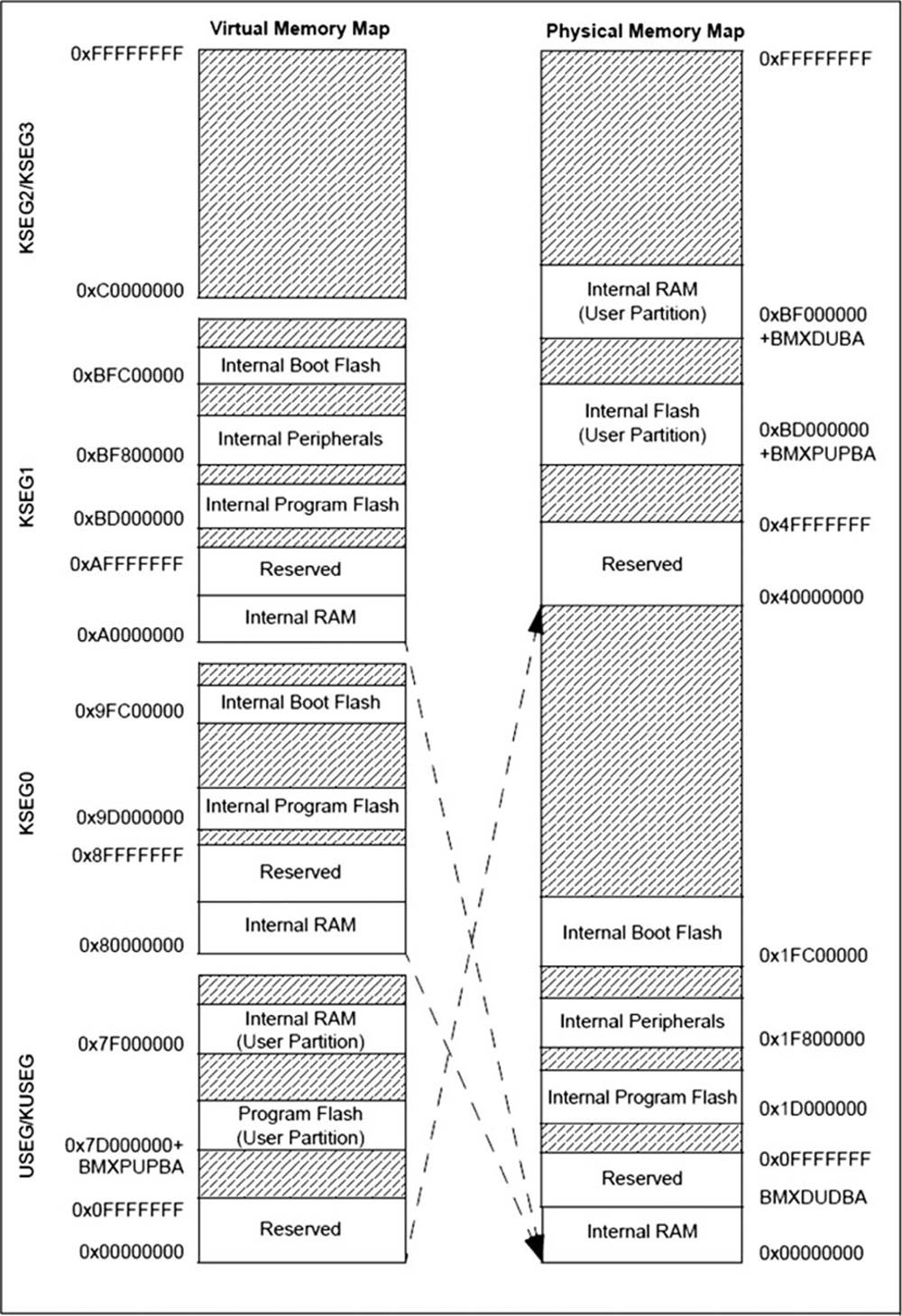
FIGURE 2.4 The Memory Structure
As can be seen from the figure, two address spaces are implemented: virtual and physical. All hardware resources, such as data memory, program memory, and DMA transfers, are handled by the physical addresses. If we wish to access the memory independent of the CPU (such as the case in DMA), then we must use the physical addresses.
Virtual addresses are important as they are used exclusively by the CPU to fetch and execute instructions. In normal programming, we are only interested with the virtual memory addresses. These addresses are translated into physical addresses by a Fixed Mapping Translation (FMT) unit inside the processor. The translation process is simply a bitwise AND of the virtual address spaces with fixed number 0x1FFFFFFF. Details of the physical address space are available in the PIC32 Family Reference Manual, or in the individual microcontroller data sheets.
The entire virtual memory address space is 4 GB and is divided into two primary regions: user mode segment and kernel mode segment. The lower 2 GB of address space forms the user mode segment (called Useg/Kuseg). The upper 2 GB of virtual address space forms the kernel mode segment. The kernel address space has been designed to be used by the operating system, while the user address space holds a user program that runs under the operating system. This is for safety, as a program in the user address space cannot access the memory space of the kernel address space. But programs in the kernel can access the user address space (this is what the “K” in name Kuser indicates). As most embedded microcontroller applications do not use an operating system, we can place all our programs and data in the kernel address space and do not use the user address space at all. As a result of this, we will have 2 GB of address space for our programs and data.
The kernel address space is divided into four segments of 512 MB each: KSEG0, KSEG1, KSEG2, and KSEG3. The kernel address space contains the following memory areas:
• Program memory (flash)
• Data memory (RAM)
• Special function registers (SFR)
• Boot memory area
The kernel virtual address space contains two identical subsections, both translated to the same physical memory addresses. One of these subsections is cacheable, while the other one is not cacheable. Here, cacheable means that the instructions and data stored in the cache can be prefetched, and this speeds up the execution time considerably in sequential operations by eliminating the need to fetch data or instructions from the memory (the cache memory is a small, very fast memory). KSEG0 corresponds to the cacheable kernel address space, while KSEG1 corresponds to the noncacheable kernel address space. Each of KSEG0 and KSEG1 contains the program memory (flash), data memory (RAM), SFR, and boot memory area. Notice that a PIC32 microcontroller can run a program that is stored in the RAM memory (as opposed to the usual case of a program stored in the flash memory).
The cacheable kernel segment is used during normal program executions where instructions and data are fetched with the cache enabled. The noncacheable kernel segment is used during the processor initialisation routines where we wish to execute the instructions sequentially and with no cache present. The prefetch cache module can be enabled under software control.
When the PIC32 microcontroller is reset, it goes to the reset address of 0xBFC00000, which is the starting address of the boot program in the noncacheable kernel segment. The code in the boot location takes care of initialisation tasks, sets configuration bits, and then calls the user-written program in the cacheable kernel segment of the memory (the user program usually, but not always, starts from address 0x9D001000 in KSEG0 space). Notice that a new PIC32 microcontroller contains no program or data when it arrives from the factory. The boot program is normally placed there by the microcontroller programmer device.
The virtual or physical memory addresses are important to programmers writing assembly code, or developing DMA routines. In normal C programs, we are not concerned with the memory addresses as the compiler and linker take care of all the program and data placements.
2.1.2. The Microcontroller Clock
The block diagram of the clock circuit of the PIC32MX microcontroller is shown in Figure 2.5.
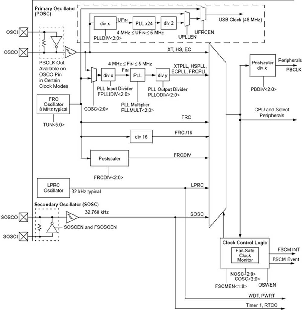
FIGURE 2.5 The PIC32MX Clock Block Diagram
There are five clock sources: two of them use internal oscillators and three require external crystals or oscillator circuits. Three clock outputs are available: CPU system clock, USB clock, and peripheral clock.
Clock sources
• FRC is an internal oscillator requiring no external components. The clock frequency is 8 MHz and is designed for medium-speed, low-power operations. The clock can be tuned via the TUN bits of register OSCTUN. The clock is accurate to about ±2% after calibration.
• LPRC is a low-frequency, low-power internal oscillator with a frequency 32 kHz, requiring no external components.
• POSC is the primary high-speed oscillator, requiring an external crystal up to 20 MHz. The crystal is connected directly to the OSCI and OSCO inputs with two capacitors.
• Secondary oscillator (SOSC) is the secondary low-speed, high-accuracy oscillator, designed for operation with a crystal of 32,768 Hz. This oscillator can be used for timer and real-time clock modules, or as the main low-speed CPU oscillator.
• EC is the external clock source, requiring no external crystal. A square wave signal is applied to this input at the required frequency.
Clock outputs
The three clock outputs can be selected in various configurations as described below (see Figure 2.5).
USB clock
The USB operation requires an exact 48 MHz clock. This clock can be derived in many different ways. Some of the methods are given as follows:
• An 8 MHz external crystal–driven primary clock (POSC), divided by 2 (using PLLDIV), and then multiplied by 24 to give 96 MHz. This frequency can then be divided by 2 to give the required 48 MHz clock. UPLLEN and UFRCEN select this clock at the output. It is important to note that the input to PLLx24 must be between 4 and 5 MHz. We can use different external crystals with different PLL divisions. For example, we can use a 4 MHz crystal with POSC, divide by 1 (using PLLDIV), and then multiply by 24 to give 96 MHz. This frequency can then be divided by 2 as above to give the required 48 MHz clock.
• An external 48 MHz primary oscillator. UPLLEN and UFRCEN select this clock at the output.
CPU clock
The main system clock can be chosen from a variety of sources shown as follows (see Figure 2.5):
• Primary clock (POSC) selected at the output directly.
• Primary clock selected through the PLL input and output dividers, and the PLL multiplier. For example, if we use 8 MHz crystal, divide by 2 (using FPLLIDIV), multiply by 16 (using PLLMULT), and divide by 2 (using PLLODIV), we get a 32 MHz clock rate.
• Internal 8 MHz clock (FRC) can be selected directly at the output to give 8 MHz. Alternatively, the clock can be divided by 16, or it can pass through a postscaler to select the required frequency.
• Internal 8 MHz clock (FRC) can be selected with the PLL. For example, this clock can be divided by 2 to give 4 MHz at the input of the PLL (remember, the input clock to PLL must be between 4 and 5 MHz); it can be multiplied by 16, and then divided by 2 to give 32 MHz at the output.
• The 32 kHz clock (LPRC) can be selected directly at the output.
• The 32,768 Hz clock (SOSC) can be selected directly at the output.
Peripheral clock
The peripheral clock (PBCLK) is derived from the CPU system clock by passing it through a postscaler. The postscaler rate can be selected as 1, 2, 4, or 8. Thus, for example, if the CPU system clock is chosen as 80 MHz, then the peripheral clock can be 80, 40, 20, or 10 MHz.
Configuring the operating clocks
The clock configuration bits shown in Figure 2.5 can be selected by programming the SFR registers (e.g., OSCCON, OSCTUN, OSCCONCLR) or the device configuration registers (e.g., DEVCFG1 and DEVCFG2) during run time.
Alternatively, the operating clocks can be selected during the programming of the microcontroller chip. Most programming devices give options to users to select the operating clocks by modifying the device configuration registers just before the chip is programmed.
The crystal connections to OSCI and OSCO pins are shown in Figure 2.6 with two small capacitors. The connection of an external clock source in EC mode is shown in Figure 2.7. In this mode, the OSCO pin can be configured either as a clock output or as an I/O port.
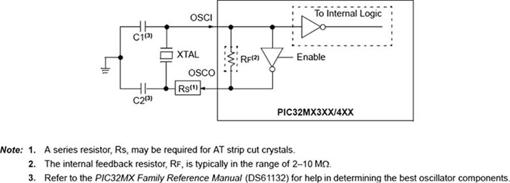
FIGURE 2.6 Crystal Connection
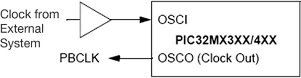
FIGURE 2.7 External Clock Connection
Performance and power consumption considerations
In microcontroller-based applications, the power consumption and performance are in direct conflict with each other. To lower the power consumption in an application, we also have to lower the performance, that is, the clock rate. Conversely, an increase in the performance also increases the power consumption. Thus, the higher the clock speed, the higher is the power consumption of the device. The designers of the PIC32 microcontroller have spent a considerable amount of time to provide a wide range of clock selection mechanisms so that the user can choose the best clock rate for the required power consumption.
For example, if an application can run at 8 MHz to do a job, there is no point in running the application at 80 MHz. In some applications, the device may be in standby mode and may be waiting for some user action (e.g., pressing a button). In such applications, a low clock rate can be selected while the device is in standby mode, and then a full high-speed clock rate can be selected when the device wakes up to run the actual application.
The flash wait states
The number of wait states is normally set by default to the highest value as this provides the safest operation. The SFR register CHECON, bits PFMWS, controls the number of wait states, and we can reduce its value for higher performance. It is important to remember, however, that setting wrong number of wait states could cause errors while accessing the flash memory. This register can take values between 0 and 7. For optimum performance, the wait states would be programmed to the minimum possible value.
2.1.3. Resets
There are several sources that can cause the microcontroller to reset. The following is a list of these sources:
• POR
• External reset (MCLR)
• Software reset (SWR)
• Watchdog timer reset (WDTR)
• BOR
• Configuration mismatch reset (CMR)
The SFR register RCON is the reset controller register, and the source of a reset can easily be found by reading the bits of this register. Any set bit in this register indicates that a reset has occurred, and depending on the position of this bit one can tell the actual source of the reset. For example, if bit 7 is set, then the source of reset is the external MCLR input (further details can be obtained from the individual microcontroller data sheets).
In this section, we are interested in external resets that are caused, for example, by the user pressing a button. The MCLR pin is used for external device reset, device programming, and device debugging. External reset occurs when the MCLR pin is lowered. Notice that the microcontroller can be reset in software by executing a specific sequence of operations (see the individual device data sheets).
2.1.4. The Input/Output Ports
The general-purpose I/O ports are very important in many applications as they allow the microcontroller to monitor and control devices attached to it. Although the I/O ports of the PIC32 microcontrollers have some similarities with the 8- and 16-bit devices, PIC32 microcontrollers offer greater functionality and new added features.
Some of the key features of PIC32 I/O ports are the following:
• Open-drain capability of each pin
• Pull-up resistors at each input pin
• Fast I/O bit manipulation
• Operation during CPU SLEEP and IDLE modes
• Input monitoring and interrupt generation on mismatch conditions
Figure 2.8 shows the basic block diagram of an I/O port.
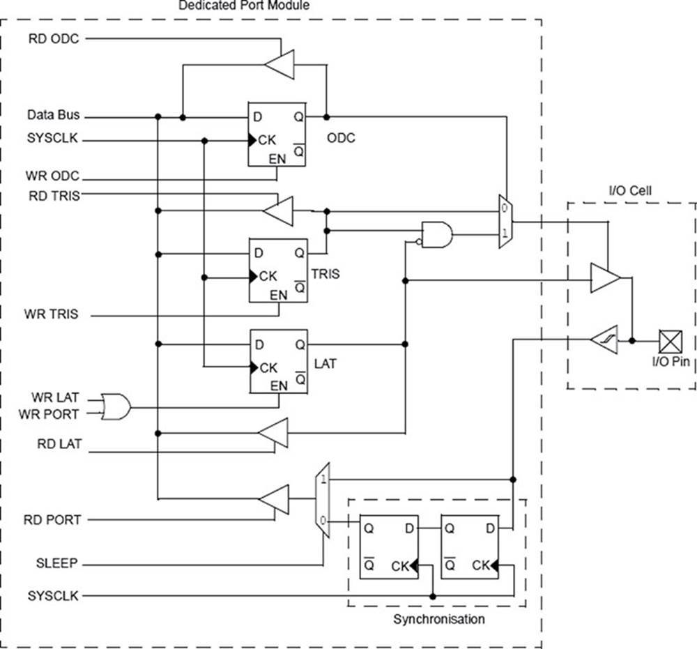
FIGURE 2.8 Block Diagram of an I/O Port
An I/O port is controlled with the following SFR registers:
• TRISx: data direction control register for port x
• PORTx: port register for port x
• LATx: latch register for port x
• ODCx: open-drain control register for port x
• CNCON: interrupt-on-change control register
TRISx
There is a TRISx register for every port x. The TRISx register configures the port signal directions. A TRISx bit set to 1 configures the corresponding port pin “x” as an input. Similarly, a TRISx bit cleared to 0 configures the corresponding port pin “x” as an output. In the example shown in Figure 2.9, odd bits (1, 3, 5, 7, 9, 11, 13, and 15) of PORTB are configured as inputs and the remaining pins as outputs.
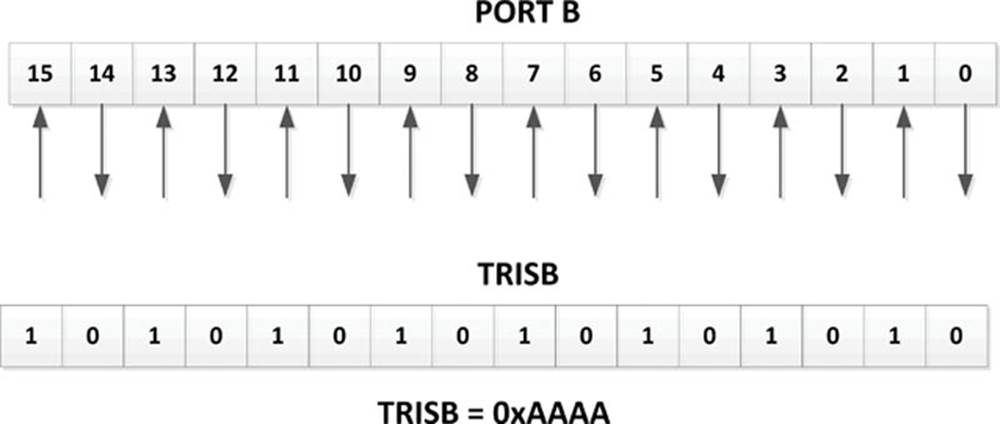
FIGURE 2.9 Example TRIS Register Setting
PORTx
PORTx are the actual port registers. A write to PORTx sends data to the port latch register LATx, and this data appears at the output of the port. A read from a PORTx register reads the actual data at the output pin of the port (the state of the output pin may be affected by a device connected to the pin).
LATx
LATx are the port latch registers. A write to a latch register is same as sending data to the port register PORTx. A read from the latch register, however, reads the data present at the output latch of the port pin, and this may not be same as the actual state of the port pin. For example, the port pin may be pulled low by an external device. Under such circumstances, the latch register will read the data held at the output latch and not the actual state of the pin.
ODCx
Each I/O output pin can be configured individually as either normal output or open-drain output. SFR register ODCx controls the output state of a pin as follows: an OCDx bit set to 1 configures the corresponding port pin “x” as open-drain. Similarly, an OCDx bit cleared to 0 configures the corresponding port pin “x” as normal digital output. The open-drain feature allows the generation of outputs higher than the supply voltage (VDD) on any desired digital output pin. Notice that external pull-up resistors are normally used on open-drain output pins. In the example in Figure 2.10, all odd-numbered (1, 3, 5, 7, 9, 11, 13, and 15) PORTB output pins are configured to be open-drain.

FIGURE 2.10 Example ODC Register Setting
CNCON
Some of the I/O pins can be configured to generate an interrupt when a change is detected on the pin. The SFR registers that control this change notice are the following:
• CNCON: used to enable or disable the interrupt-on-change (change notice) feature
• CNENx: contains the control bits, where “x” is the number of the change notice pin
• CNPUEx: enables or disables pull-up resistors on port pin “x”
Notice that bit CNIE (bit 0) of the IEC1 SFR register must be set to 1 to enable interrupt-on-change feature.
SET, CLR, INV I/O port registers
In addition to the I/O port registers described in this section, each port register has SET, CLR, and INV registers associated with it that can be useful in bit manipulation operations, allowing faster operations to be carried out.
The following registers are available for bit manipulation:
• TRISxSET
• TRISxCLR
• TRISxINV
• PORTxSET
• PORTxCLR
• PORTxINV
• LATxSET
• LATxCLR
• LATxINV
• ODCxSET
• ODCxCLR
• ODCxINV
• CNCONSET
• CNCONCLR
• CNCONINV
• CNPUESET
• CNPUECLR
• CNPUEINV
An example is given below to show how the SET, CLR, and INV registers can be used on TRISB register. Use of other registers is similar and is not repeated here.
Register TRISBCLR is a write-only register, and it clears selected bits in TRISB register. Writing a 1 in one or more bit positions clears the corresponding bits in TRISB register. Writing a 0 does not affect the register. For example, to clear bits 15, 5, and 0 of TRISB register, we issue the command: TRISBCLR = 0b1000000000100001 or TRSBCLR = 0x08021.
Register TRISBSET is a write-only register, and it sets selected bits in TRISB register. Writing a 1 in one or more bit positions sets the corresponding bits in TRISB register. Writing a 0 does not affect the register. For example, to set bits 15, 5, and 0 of TRISB register, we issue the command: TRISBSET = 0b1000000000100001 or TRSBSET = 0x08021.
Register TRISBINV is a write-only register, and it inverts selected bits in TRISB register. Writing a 1 in one or more bit positions inverts the corresponding bits in TRISB register. Writing a 0 does not affect the register. For example, to invert bits 15, 5, and 0 of TRISB register, we issue the command: TRISBINV = 0b1000000000100001 or TRSBINV = 0x08021.
Digital/analogue inputs
By default, all I/O pins are configured as analogue inputs. Setting the corresponding bits in the AD1PCFG register to 0 configures the pin as an analogue input, independent of the TRIS register setting for that pin. Similarly, setting a bit to 1 configures the pin as digital I/O. For example, to set all analogue pins as digital, we have to issue the command AD1PCFG = 0xFFFF.
It is recommended that any unused I/O pins that are not used should be set as outputs (e.g., by clearing the corresponding TRIS bits) and cleared to Low in software. When attaching devices to an I/O port, it is important to note with care that the normal I/O voltage of a pin is 3.6 V. An input pin can tolerate an input voltage up to 5 V, but the output voltage from an output pin cannot exceed 3.6 V.
2.1.5. The Parallel Master Port (PMP)
The PMP is an 8/16-bit parallel I/O port that can be used to communicate with a variety of parallel devices such as microcontrollers, external peripheral devices, LCDs, GLCDs, and so on. In this section, we will briefly look at the operation of the PMP. Further details about the PMP can be obtained from individual device data sheets.
Most microcontroller-based applications require address and data lines, and chip select control lines. The PMP provides up to 16 address and data lines, and up to 2 chip select lines. Addresses can be autoincremented and autodecremented for greater flexibility. In addition, parallel slave port support and individual read and write strobes are provided. Figure 2.11 shows a typical application of the PMP to interface to an external EPROM memory.
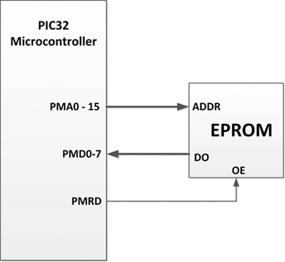
FIGURE 2.11 Using PMP With External EPROM Memory
There are a number of SFR registers used to control the PMP. These are summarised as follows:
• PMCON: PMP control register
• PMMODE: PMP mode control register
• PMADDR: PMP address register
• PMDOUT: PMP data output register
• PMDIN: PMP data input register
• PMAEN: PMP address enable register
• PMSTAT: PMP status register
Each register has bit manipulation options. Thus, for example, in addition to PMCON, there are registers named PMCONCLR, PMCONSET, and PMCONINV.
PMCON
Register PMCON controls the PMP module. Figures 2.12 and 2.13 show the PMCON bit configuration and bit definitions, respectively. The bits in PMCON control address multiplexing, enable port control signals, enable chip select signals, and select signal polarity.
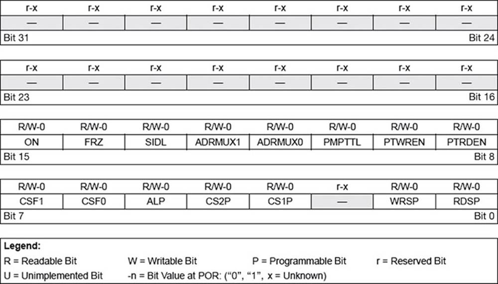
FIGURE 2.12 PMCON Register Bit Configuration
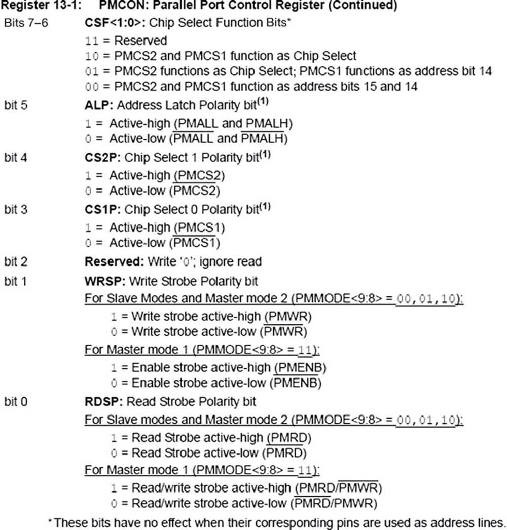
FIGURE 2.13 PMCON Bit Definitions
PMMODE
Register PMMODE controls the operational modes of the PMP. Figures 2.14 and 2.15 show the PMMODE bit configuration and bit definitions, respectively.
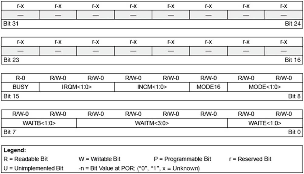
FIGURE 2.14 PMMODE Register Bit Configuration
FIGURE 2.15 PMMODE Bit Definitions
PMADDR
Register PMADDR contains address of the external device and the chip select control bits. Figure 2.16 shows the PMADDR bit configuration and bit definitions.
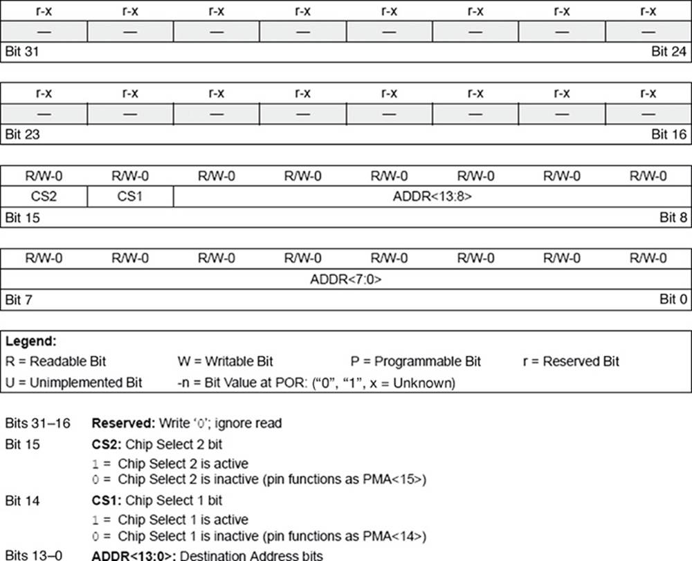
FIGURE 2.16 PMADDR Register Bit Configuration and Bit Definitions
PMDOUT
Register PMDOUT controls the buffered data output in slave mode. Figure 2.17 shows the bit configuration and bit definitions.
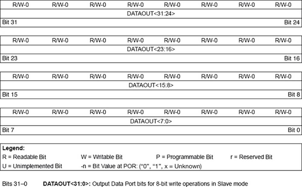
FIGURE 2.17 PMDOUT Register Bit Configuration and Bit Definitions
PMDIN
This register controls the I/O data ports in 8/16-bit master mode, and input data port in 8-bit slave mode. Figure 2.18 shows the bit configuration and bit definitions.
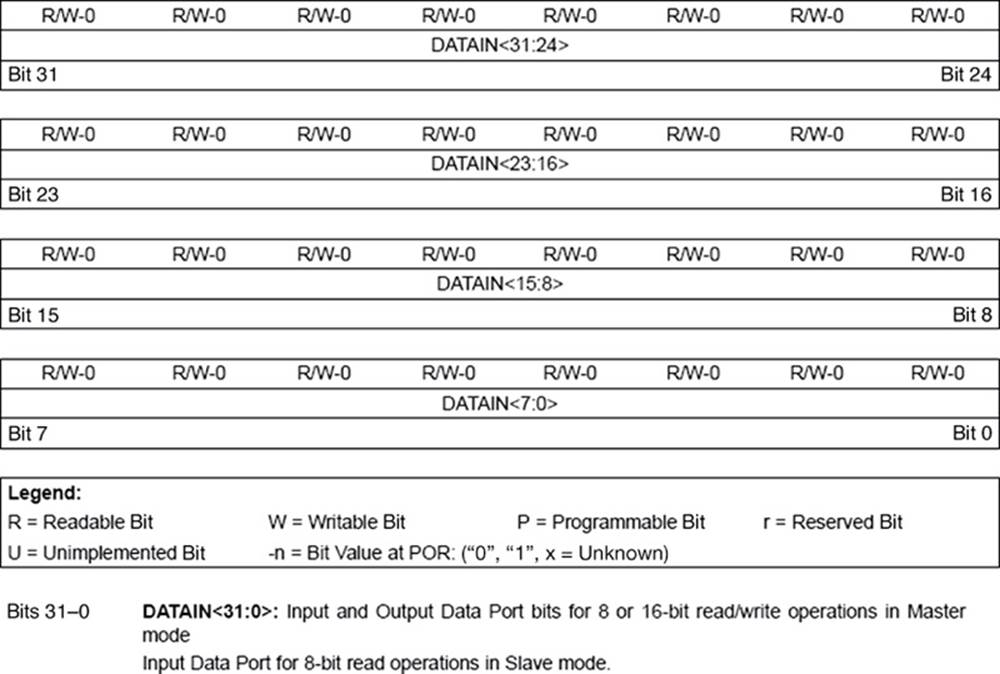
FIGURE 2.18 PMDIN Register Bit Configuration and Bit Definitions
PMAEN
This register controls the operation of address and chip select pins of the PMP module. Figure 2.19 shows the bit configuration and bit definitions.
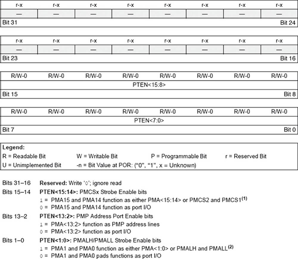
FIGURE 2.19 PMAEN Register Bit Configuration and Bit Definitions
PMSTAT
This register contains the status bits when operating in buffered mode. Figures 2.20 and 2.21 show the bit configuration and bit definitions, respectively.
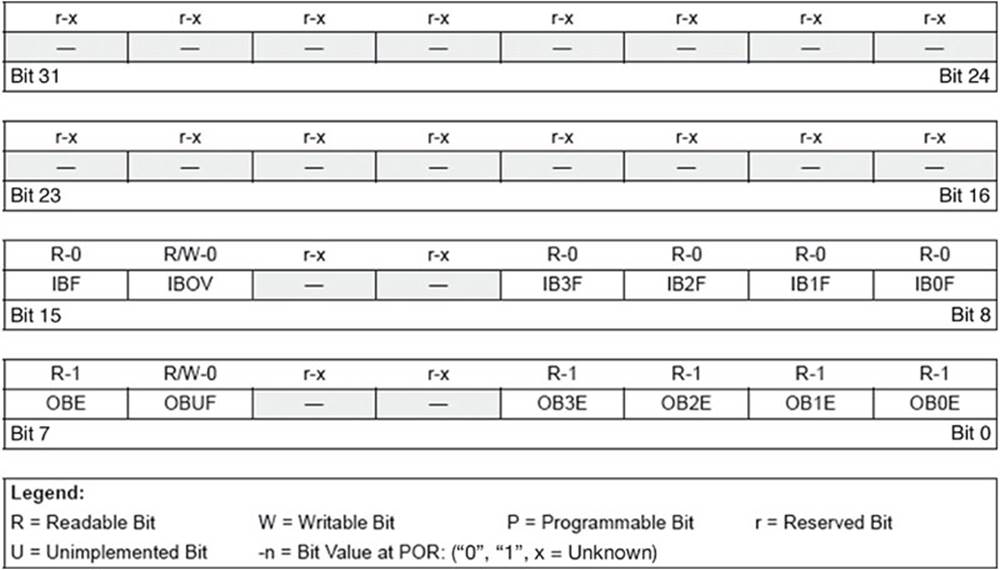
FIGURE 2.20 PMSTAT Register Bit Configuration
FIGURE 2.21 PMSTAT Register Bit Definitions
2.1.6. Timers
The PIC32 microcontroller supports five timers, named TIMER1–TIMER5. Timer 1 is 16-bit wide, while the other timers can be combined for 32-bit operation. In this section, we will look at the operation of Timer 1.
Timer 1
Timer 1 is 16-bit wide that can be used in various internal and external timing and counting applications. This timer can be used in synchronous and asynchronous internal and external modes.
Figure 2.22 shows the block diagram of Timer 1. The source of clock for Timer 1 can be from the low-power SOSC, from the external input pin T1CK, or from the peripheral bus clock (PBCLK). A prescaler is provided with division ratios of 1, 8, 64, and 256 in order to change the timer clock frequency. The operation of the timer is given in the following paragraphs.
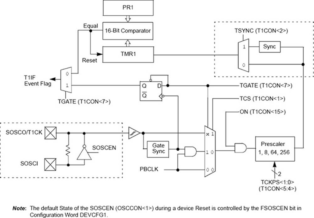
FIGURE 2.22 Timer 1 Block Diagram
Timer register PR1 is loaded with a 16-bit number. Register TMR1 counts up at every clock pulse, and when PR1 is equal to TMR1, timer flag T1IF is set. At the same time, register TMR1 is reset to zero so that new count starts from zero again. If Timer 1 interrupts are enabled, then an interrupt will be generated where the program will jump to the interrupt service routine (ISR) whenever the timer flag is set.
Timer 1 is controlled by three registers: T1CON, PR1, and TMR1. Figures 2.23 and 2.24 show the bit configuration and bit definitions of register T1CON, respectively.
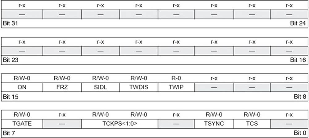
FIGURE 2.23 T1CON Bit Configuration
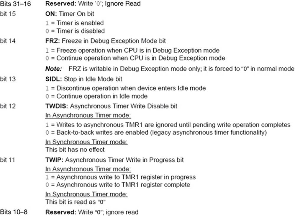
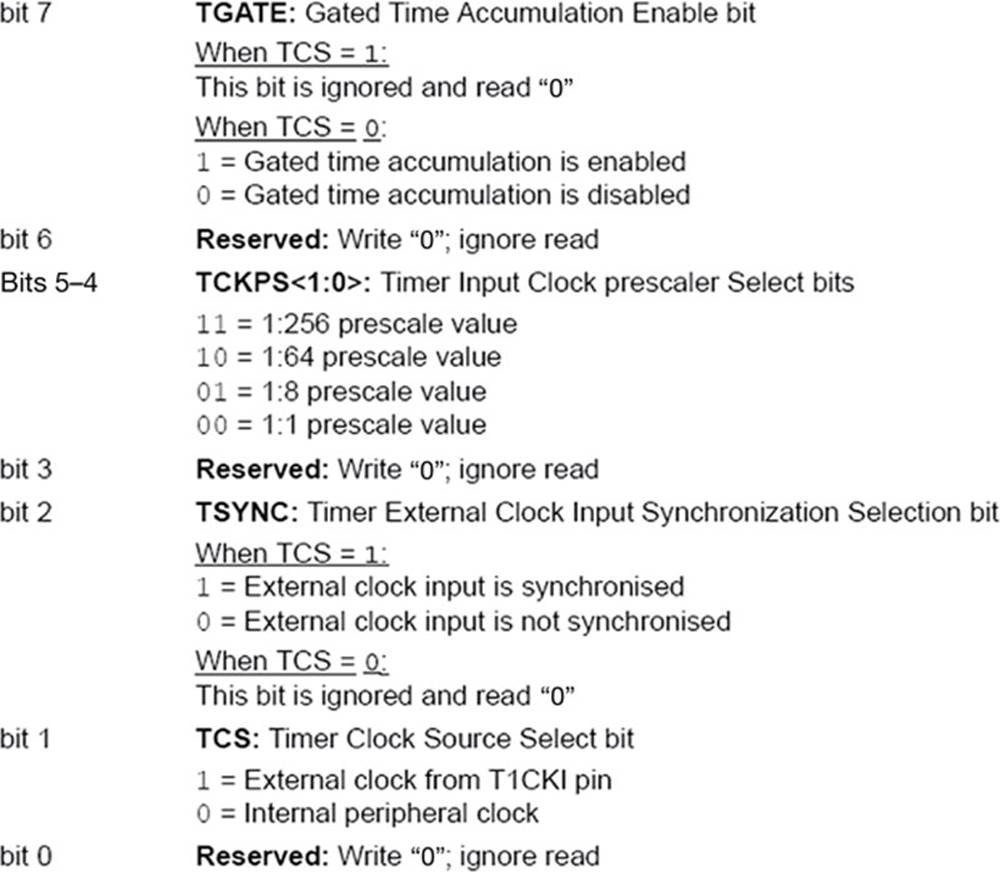
FIGURE 2.24 T1CON Bit Definitions
Assuming TMR1 starts counting from 0, the delay before the count reaches to PR1 is given by the following equation:
![]()
where T is the clock period and PR1 is the value loaded into register PR1. Rearranging the above equation, we can find the value to be loaded into PR1 as:

An example is given here to illustrate the process. Assume that the clock frequency is 20 MHz, and it is required to generate a timer interrupt every 256 ms. Assuming a prescaler value of 256, the value to be loaded into PR1 is calculated as:
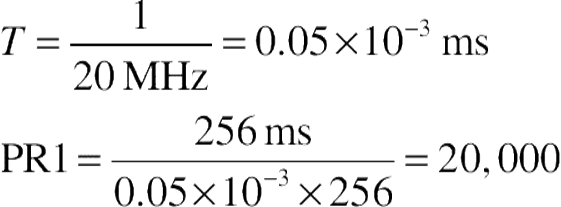
Thus, the required settings are:
TMR1 = 0
Prescaler = 256
PR1 = 20,000 (0x4E20)
The steps to configure Timer 1 are summarised as follows (assuming no timer interrupts are required):
• Disable Timer 1 (T1CON, bit 15 = 0).
• Select required prescaler value (T1CON, bits 4–5).
• Select timer clock (T1CON, bit 1).
• Load PR1 register with required value.
• Clear TMR1 register to 0.
• Enable the timer (T1CON, bit 15 = 1).
An example project is given in the Projects section of this book to show how to configure Timer 1 with interrupts.
Timers 2, 3, 4, 5
Although Timers 2, 3, 4, and 5 can operate as 16-bit timers, Timers 2 and 3, and Timers 4 and 5 can be combined to provide two 32-bit wide internal and external timers.
Figure 2.25 shows the block diagram of these timers in 16-bit mode (note that “x” represents the timer number and is between 2 and 5). Notice that, compared with Timer 1, the prescaler has been extended and the low-power SOSC has been removed. The operation of these timers in 16-bit mode is same as that of Timer 1.
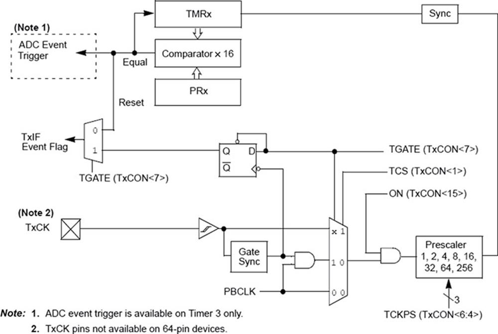
FIGURE 2.25 Timers 2, 3, 4, and 5 in 16-Bit Mode
Figure 2.26 shows the timers in 32-bit mode where Timers 2/3 and 4/5 are combined (in this figure “x” represents Timers 2–5 in 16-bit mode, while in 32-bit mode “x” represents Timer 2 or 4, while “y” represents Timer 3 or 5).
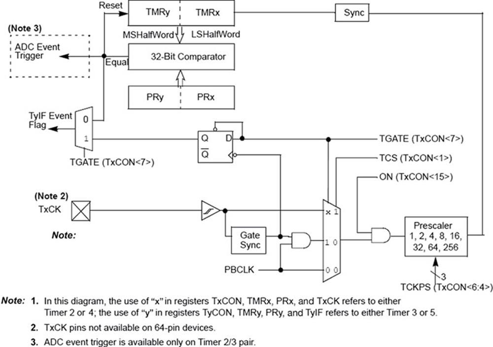
FIGURE 2.26 Timers 2/3 and 4/5 Combined for 32-Bit Operation
Considering, for example, Timers 2 and 3 in 32-bit operation, register PR3 and PR2 are combined to form a 32-bit register. Similarly, registers TMR3 and TMR2 are combined to form a 32-bit register. A 32-bit comparator is used to compare the two pairs and generate the T3IF flag when they are equal. In 32-bit mode, Timer 2/3 pair is controlled with register T2CON. Similarly, Timer 4/5 pair is controlled with register T4CON.
The steps to configure Timer 2/3 are summarised as follows (assuming no timer interrupts are required):
• Disable Timer 1 (T2CON, bit 15 = 0).
• Set 32-bit mode (T2CON, bit 3 = 1).
• Select required prescaler value (T2CON, bits 4–6).
• Select internal timer clock (T2CON, bit 1 = 0).
• Clear timer registers TMR2 and TMR3.
• Load PR2 and PR3 registers with required value.
• Clear TMR1 register to 0.
• Enable the timer (T2CON, bit 15 = 1).
2.1.7. Real-Time Clock and Calendar
The RTCC module is intended for accurate real-time date and time applications. Some of the features of this module are:
• Provides real-time hours, minutes, seconds, weekday, date, month, and year
• Provides alarm intervals for 0.5, 1, 10 s, 1, 10 min, 1 h, 1 day, 1 week, 1 month, and 1 year
• Provides leap year correction
• Provides long-term battery operation
• Provides alarm pulse on output pin
• Requires an external 32,768 Hz crystal
Figure 2.27 shows a block diagram of the RTCC module. The module is controlled by the following six SFR registers:
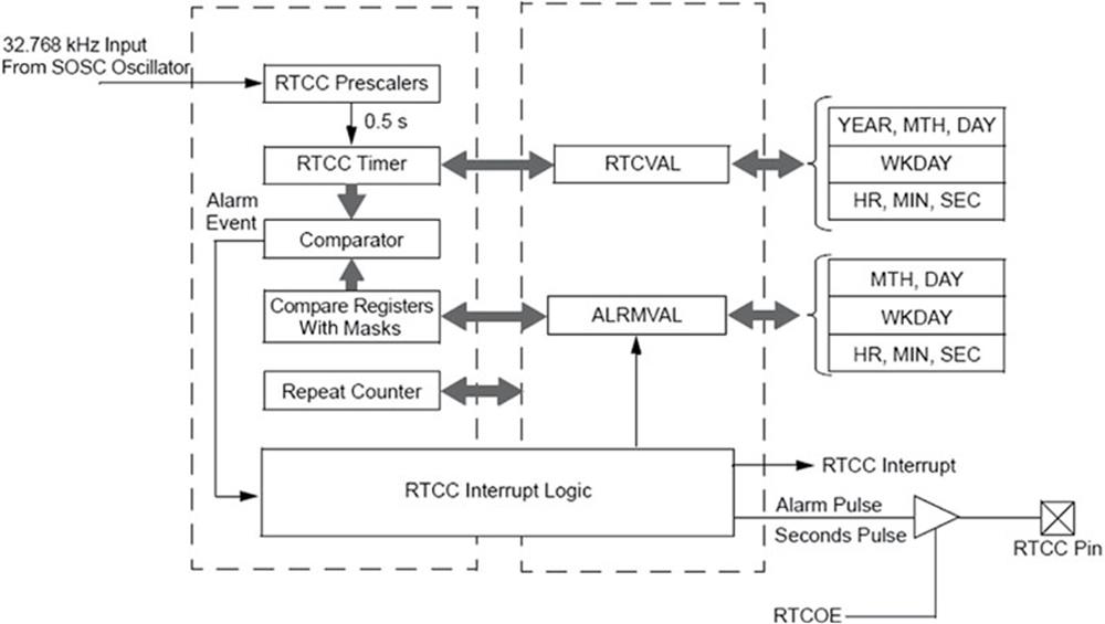
FIGURE 2.27 Block Diagram of the RTCC Module
• RTCCON
• RTCALRM
• RTCTIME
• RTCDATE
• ALRMTIME
• ALRMDATE
Interested readers can find the programming details of the RTCC module in the individual microcontroller data sheets.
2.1.8. Analogue-to-Digital Converter
The PIC32MX460F512L microcontroller contains multiplexed 16-channel, 10-bit A/D converters. These converters have the following features:
• 500 ksps (kilo samples per second) conversion speed
• Multiplexed 16 channels (2 switchable multiplexers to select different analogue channels and different reference sources)
• Sample-and-hold amplifier (SHA)
• Automatic input channel scanning
• 32-Bit wide, 16-word result buffer
• Various conversion result formats (integer, signed, unsigned, 16- or 32-bit output)
• External voltage references
• Operation during CPU SLEEP and IDLE modes
Figure 2.28 shows a block diagram of the ADC converter module.
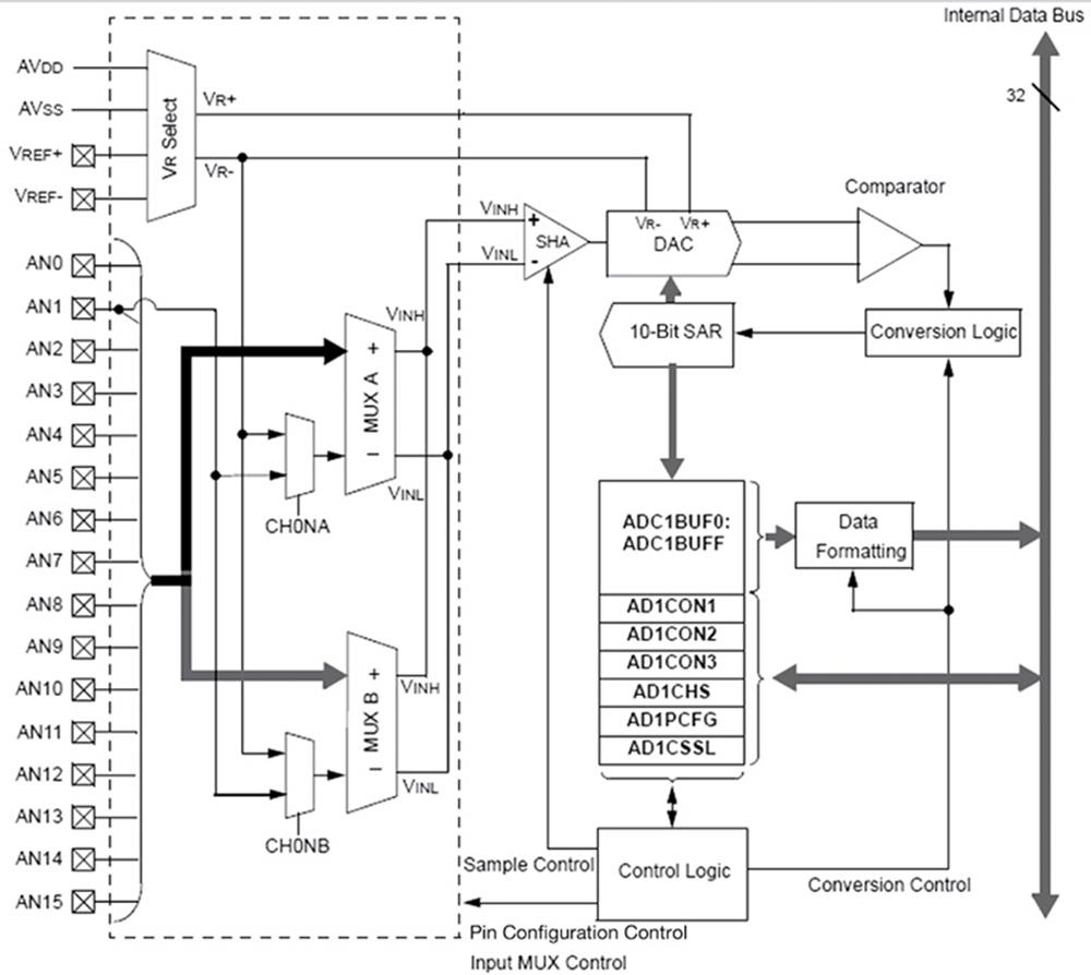
FIGURE 2.28 ADC Converter Module
The ADC converter module is controlled by the following SFR registers:
• AD1CON1
• AD1CON2
• AD1CON3
• AD1CHS
• AD1PCFG
• AD1CSSL
In addition, all the above registers have additional bit manipulation registers, for example, AD1CON1CLR, AD1CON1SET, and AD1CON1INV.
AD1CON1
This register controls the ADC operating mode, data output format, conversion trigger source select, sample and hold control, and ADC conversion status. Figures 2.29 and 2.30 show the AD1CON1 bit configuration and bit definitions, respectively.
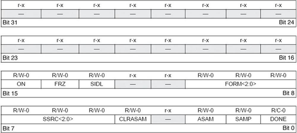
FIGURE 2.29 AD1CON1 Bit Configuration
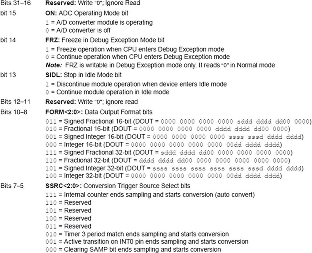
FIGURE 2.30 AD1CON1 Bit Definitions
AD1CON2
This register controls the voltage reference selection, scan input selection, ADC interrupt selection bits, ADC result buffer configuration, and alternate input sample mode selection. Figures 2.31 and 2.32 show the AD1CON2 bit configuration and bit definitions, respectively.
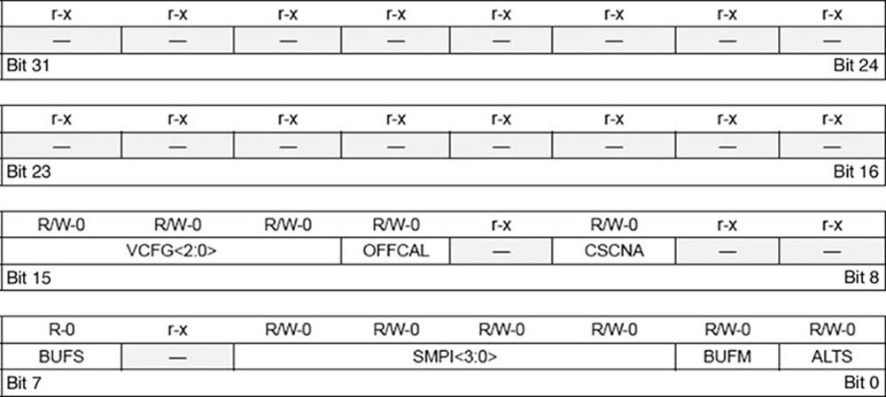
FIGURE 2.31 AD1CON2 Bit Configuration
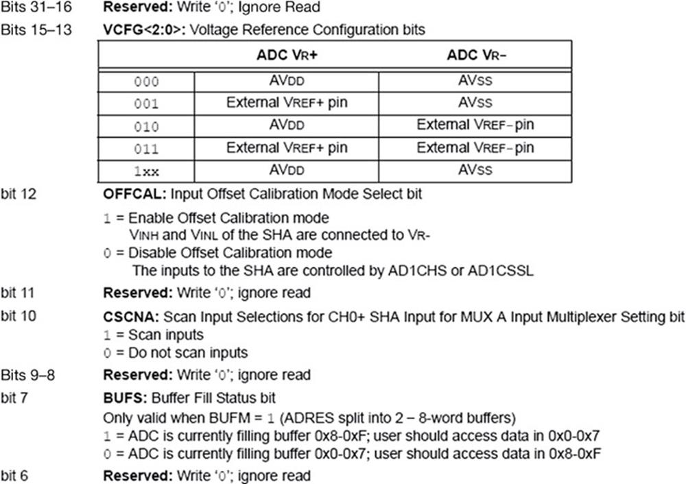
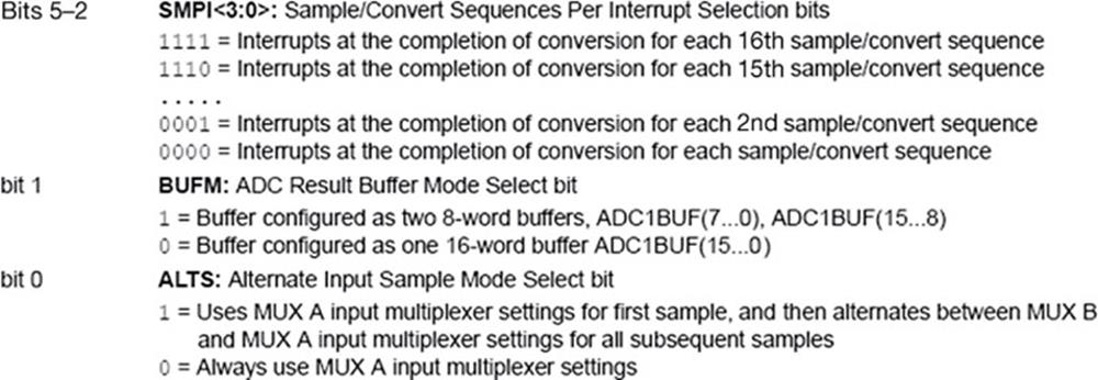
FIGURE 2.32 AD1CON2 Bit Definitions
AD1CON3
This register controls the ADC clock selection. Figure 2.33 shows the bit configuration and bit definitions.
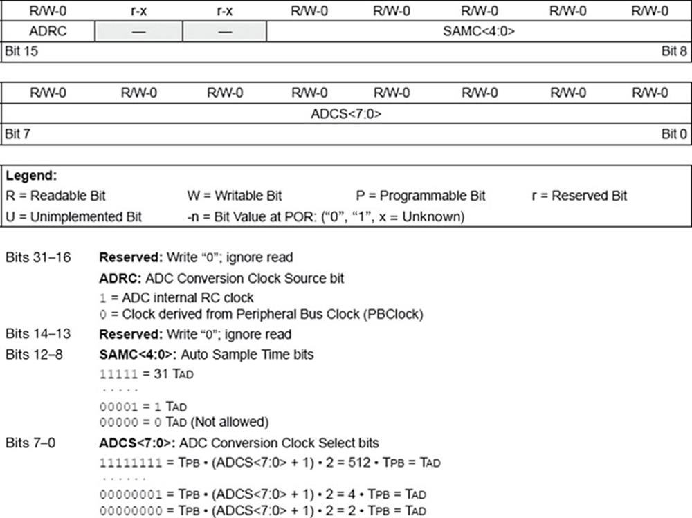
FIGURE 2.33 AD1CON3 Bit Configuration and Bit Definitions
AD1CHS
This register selects the input channels for multiplexers A and B. Figures 2.34 and 2.35 show the bit configuration and bit definitions, respectively.
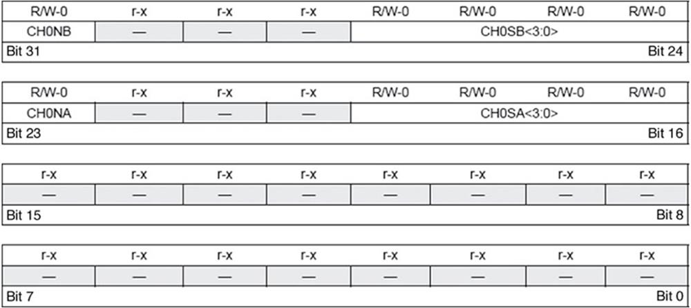
FIGURE 2.34 AD1CHS Bit Configuration
FIGURE 2.35 AD1CHS Bit Definitions
AD1PCFG
This register selects the input ports as analogue or digital. Setting a bit to 1 makes the corresponding ANx port pin a digital port. Similarly, clearing a bit to 0 makes the corresponding ANx port pin an analogue port. To configure all analogue ports as digital, issue the command AD1PCFG = 0xFFFF. Similarly, to configure ports as analogue, issue the command AD1PCFG = 0.
AD1CSSL
This register controls the ADC input scanning. Setting a bit of the register to 1 selects the corresponding ANx port pin for input scan. Similarly, clearing a bit of the register to 0 does not select the corresponding ANx port pin for input scan.
Operation of the ADC module
The total ADC conversion time consists of the acquisition time and the ADC conversion time. The ADC has a single SHA. During the acquisition time, the analogue signal is sampled and held by the SHA. After the input is stable, it is disconnected from the SHA and the ADC conversion starts, which converts the analogue signal into digital. The conversion time is the actual time it takes the ADC converter to convert the signal held by the SHA. Although there is only one SHA, there are two multiplexers called MUXA and MUXB, controlled by register AD1CHS. The ADC converter can switch between MUXA and MUXB inputs.
The converted data in the result register can be read in eight different formats, controlled by AD1CON1.
Sampling can be started manually or automatically. In manual mode, bit 2 of AD1CON1 is cleared. Data acquisition is started when bit 1 of AD1CON1 is set. This bit must be set to restart acquisition. In automatic mode, bit 2 of AD1CON is set, and acquisition starts automatically after a previous sample has completed.
The scan mode enables a number of input channels to be scanned and converted into digital. This mode is enabled by setting bit 10 of AD1CON2. Each bit in the AD1CSSL register corresponds to an analogue input channel, and if a bit is set to 1 in AD1CSSL, then the corresponding input channel is in the scan sequence.
The following steps summarise how to configure the ADC module, assuming no interrupts are to be generated (see the individual microcontroller data sheets for more information):
• Configure port pin as analogue by clearing the appropriate bits of AD1PCFG.
• Select the required analogue input channels using AD1CHS.
• Select the format of the result data using bits 8–10 of AD1CON1.
• Select the sample clock source using bits 5–7 of AD1CON1.
• Select the voltage reference source using bits 13–15 of AD1CON2.
• Select the scan mode (if required), alternating sample mode (if required), and autoconvert sample time (if required).
• Select the result buffer mode using bit 1 of AD1CON2.
• Select the A/D clock source using bit 15 of AD1CON3.
• Select A/D clock prescaler using bits 0–7 of AD1CON3.
• Turn ON the A/D using bit 15 of AD1CON1.
Most high-level compilers provide a built-in library for simple one-channel ADC conversions, where all the required registers are set automatically.
2.1.9. Interrupts
Interrupt control is one of the most complex parts of the PIC32 microcontrollers. There are 96 interrupt sources with up to 64 interrupt vectors, and a large number of interrupt control registers. The full description of the interrupt control is beyond the scope of this book, and interested readers should consult the individual microcontroller data sheets for much more information.
In this section, we shall be looking at the basic operation of the interrupt module and see how an interrupt-based program can be written using the mikroC PRO for PIC32 language.
The basic features of the PIC32 interrupt controller module are the following:
• Up to 96 interrupt sources
• Up to 64 interrupt vectors
• Single and multiple vector interrupt modes
• Seven user-selectable priority levels for each interrupt
• Four user-selectable subpriority levels within each priority
• User-configurable interrupt vector table location and spacing
The interrupt control module has the following SFR registers:
• INTCON
• INSTAT
• IPTMR
• IFS0, IFS1
• IEC0, IEC1
• IPC0–IPC11
In addition, all the above registers have additional bit manipulation registers, for example, INTCONCLR, INTCONSET, and INTCONINV. Register INTCON controls the interrupt vector mode and external interrupt edge mode. Other registers control the individual interrupt sources, such as enabling and disabling them.
PIC32 microcontrollers support both single and multiple vectored interrupts. In single vectored interrupts, all interrupting devices have the same common ISR addresses. The source of the interrupt is then determined by examining the interrupt flags of each interrupting source. This is actually the commonly used method in 8-bit microcontrollers. In multiple vectored interrupt operations, each interrupting device has its unique ISR address. (In actual fact, PIC32 microcontrollers have 96 interrupt sources and only 64 vectors. As such, some of the interrupts share the same vector.)
PIC32 microcontrollers support seven levels of interrupt priority (ipl1–ipl7). If more than one interrupt occurs at the same time, then the one with higher priority is serviced first. If while servicing an interrupt, a lower-priority interrupt occurs, then it will be ignored by the processor. In addition to standard interrupt priority levels, the PIC32 microcontrollers support four levels of subpriorities. Thus, should two interrupts at the same priority level interrupt at the same time, the one with the higher subpriority level will be serviced first. At reset or power-up, all interrupts are disabled and set to priority level ipl0.
In addition to general interrupt configuration bits, each interrupt source has associated control bits in the SFR registers, and these bits must be configured correctly for an interrupt to be accepted by the CPU. Some of the important interrupt source control bits are the following:
• Each interrupting source has an interrupt enable bit (denoted by suffix -IE) in the device data sheet. This bit must be set to 1 for an interrupt to be accepted from this source (at reset or power-up, all interrupt enable bits are cleared). Some commonly used interrupt enable bits are given in the following table:
|
Interrupt Source |
Interrupt Enable Bit |
Bit Position |
Register |
|
Timer 1 |
T1IE |
4 |
IEC0 |
|
External Int 0 |
INT0IE |
3 |
IEC0 |
|
External Int 1 |
INT1IE |
7 |
IEC0 |
|
External Int 2 |
INT2IE |
11 |
IEC0 |
|
External Int 3 |
INT3IE |
15 |
IEC0 |
• Each interrupting source has an interrupt flag (denoted by -IF) in the device data sheet. This bit is set automatically when an interrupt occurs, and must be cleared in software before any more interrupts can be accepted from the same source. The bit is usuallycleared inside the ISR of the interrupting source. The interrupt flags of some commonly used interrupt sources are given as follows:
|
Interrupt Source |
Interrupt Flag Bit |
Bit Position |
Register |
|
Timer 1 |
T1IF |
4 |
IFS0 |
|
External Int 0 |
INT0IF |
3 |
IFS0 |
|
External Int 1 |
INT1IF |
7 |
IFS0 |
|
External Int 2 |
INT2IF |
11 |
IFS0 |
|
External Int 3 |
INT3IF |
15 |
IFS0 |
• Each interrupting source has a priority level from 1 to 7 (priority level 0 disabled the interrupt), and subpriority levels from 0 to 3. The priority levels are denoted by suffix -IP, and the subpriority levels by suffix -IS. The priority levels of some commonly used interrupt sources are given as follows:
|
Interrupt Source |
Interrupt Priority Level |
Bit Positions |
Register |
|
Timer 1 |
T1IP |
2–4 |
IPC1 |
|
External Int 0 |
INT0IP |
26–28 |
IPC0 |
|
External Int 1 |
INT1IP |
26–28 |
IPC1 |
|
External Int 2 |
INT2IP |
26–28 |
IPC2 |
|
External Int 3 |
INT3IP |
26–28 |
IPC3 |
|
Interrupt Source |
Interrupt Subpriority Level |
Bit Positions |
Register |
|
Timer 1 |
T1IS |
0–1 |
IPC1 |
|
External Int 0 |
INT0IS |
24–25 |
IPC0 |
|
External Int 1 |
INT1IS |
24–25 |
IPC1 |
|
External Int 2 |
INT2IS |
24–25 |
IPC2 |
|
External Int 3 |
INT3IS |
24–25 |
IPC3 |
Some examples are given in the following to show how the timer interrupts and external interrupts can be configured. The Projects section of this book gives real examples on configuring and using both timer and external interrupts.
Configuring Timer 1 interrupts
Timer 1 counts up until the value in TMR1 matches the one in period register PR1, and then the interrupt flag T1IF is set automatically. If the Timer 1 interrupt enable flag T1IE is set, then an interrupt will be generated to the processor. In multi-interrupt operations, it is recommended to set the priority and subpriority levels of the timer interrupt.
The steps in configuring the Timer 1 interrupts are given as follows:
• Configure for single vector or multivector interrupt mode (by default, after reset or power-up the single vector mode is selected).
• Disable Timer 1, ON (bit 15 in T1CON).
• Clear timer register TMR1 to 0.
• Select timer prescaler (bits 4–5 in T1CON).
• Select timer clock source, TCS (bit 1 in T1CON).
• Load period register PR1 as required.
• Clear interrupt flag, T1IF (bit 4 in IFS0).
• Set Timer 1 priority level, T1IP (bits 2–4 in IPC1).
• Set Timer 1 subpriority level, T1IS (if required).
• Enable Timer 1 interrupts, T1IE (bit 4 in IEC0).
• Enable Timer 1, ON (bit 15 in T1CON).
• Write the ISR.
• Enable interrupts.
Configuring external interrupt 0
The PIC32 microcontroller supports four external interrupts inputs, INT0–INT3. Interrupts can be recognised on either the low-to-high or the high-to-low transition of the interrupt pin, selected by INTCON. External interrupt flag INT0IF must be cleared before an interrupt can be accepted. In addition, INT0IE bit must be set to enable interrupts from external interrupt INT0 pin. In multi-interrupt operations, it is recommended to set the priority and subpriority levels of the interrupt.
The steps in configuring the external interrupt 0 are given as follows:
• Configure for single vector or multivector interrupt mode (bit 12, INTCON). By default, after reset or power-up the single vector mode is selected.
• Clear external interrupt 0 flag, INT0IF (bit 3 in IFS0).
• Set required interrupt edge, INT0EP (bit 0 in INTCON).
• Set external interrupt 0 priority level, INT0IP (bits 26–28 in IPC0).
• Set external interrupt subpriority level, INT0IS (if required).
• Enable external interrupt 0, INT0IE (bit 3 in IEC0).
• Write the ISR.
• Enable interrupts.
PIC32 interrupt service routines
The PIC32 microcontroller interrupt controller can be configured to operate in one of the following two modes:
• Single vector mode: All interrupt requests will be serviced at one vector address (mode out of reset).
• Multivector mode: Interrupt requests will be serviced at the calculated vector address.
In single vector mode, the CPU always vectors to the same address. This means that only one ISR can be defined. The single vector mode address is calculated by using the exception base (EBase) address (its address default is 0x9FC01000E). The exact formula for single vector mode is as follows (see the PIC32 microcontroller individual data sheets for more information):
![]()
In multivector mode, the CPU vectors to the unique address for each vector number. Each vector is located at a specific offset, with respect to a base address specified by the EBase register in the CPU. The individual vector address offset is determined by the following equation:
![]()
The PIC32 family of devices employs two register sets: a primary register set for normal program execution and a shadow register set for highest-priority interrupt processing.
• Register set selection in single vector mode: In single vector mode, you can select which register set will be used. By default, the interrupt controller will instruct the CPU to use the first register set. This can be changed later in the code.
• Register set selection in multivector mode: When a priority level interrupt matches a shadow set priority, the interrupt controller instructs the CPU to use the shadow set. For all other interrupt priorities, the interrupt controller instructs the CPU to use the primary register set.
In order to correctly utilise interrupts and correctly write the ISR code, the user will need to take care of the following:
1. Write the ISR.
2. Initialise the module that will generate an interrupt.
3. Set the correct priority and subpriority for the used module according to the priorities set in the ISR.
4. Enable interrupts.
2.2. Summary
This chapter has described the architecture of the PIC32 family of microcontrollers. PIC32MX360F512L was taken as a typical example microcontroller in the family.
Various important parts and peripheral circuits of the PIC32 series of microcontrollers have been described, including the data memory, program memory, clock circuits, reset circuits, general-purpose timers, ADC converter, and the very important topic of interrupt structure. Steps are given to show how the timer and external interrupts can be configured.
2.3. Exercises
1. Describe the memory structure of the PIC32 series of microcontrollers. What is the difference between physical and virtual addresses?
2. Explain the functions of the boot memory in a PIC32 series of microcontroller.
3. Explain the differences between a general-purpose register (GPR) and a special function register (SFR).
4. Explain the various ways that the PIC32 series of microcontrollers can be reset. Draw a circuit diagram to show how an external push-button switch can be used to reset the microcontroller.
5. Describe the various clock sources that can be used to provide clock to a PIC32 series of microcontroller. Draw a circuit diagram to show how a 10 MHz crystal can be connected to the microcontroller.
6. Explain how an external clock can be used to provide clock pulses to a PIC32 series of microcontroller.
7. What are the registers of a typical I/O port in a PIC32 series of microcontroller? Explain the operation of the port by drawing the port block diagram.
8. Explain the differences between the PORT and LAT registers.
9. Explain the structure of the ADC converter of a PIC32 series of microcontroller.
10. An LM35DZ-type analogue temperature sensor is connected to analogue port AN0 of a PIC32MX460F512L microcontroller. The sensor provides an analogue output voltage proportional to the temperature, that is, Vo = 10 mV/°C. Show the steps required to read the temperature.
11. Explain the differences between a priority interrupt and a nonpriority interrupt.
12. Explain the differences between a single vector interrupt and a multivector interrupt.
13. Show the steps required to configure Timer 1 to generate an interrupt. Assuming a 10 MHz clock frequency, what will be loaded into register PR1 to generate an interrupt every second?
14. Show the steps required to set up external interrupt input INT0 to generate interrupts on its falling edge.
15. Show the steps required to set up Timer 1 to generate interrupts every millisecond having a priority of 7, and subpriority 3.
16. In an application, the CPU registers have been configured to accept interrupts from external sources INT0, INT1, and INT2. An interrupt has been detected. Explain how you can find the source of the interrupt.
All materials on the site are licensed Creative Commons Attribution-Sharealike 3.0 Unported CC BY-SA 3.0 & GNU Free Documentation License (GFDL)
If you are the copyright holder of any material contained on our site and intend to remove it, please contact our site administrator for approval.
© 2016-2026 All site design rights belong to S.Y.A.