PIC32 Microcontrollers and the Digilent chipKIT: Introductory to Advanced Projects (2015)
Chapter 4. The Cerebot MX3cK (chipKIT MX3) Development Board
Abstract
This chapter is about the chipKIT MX3 development board. It describes the board layout, power supply options, board jumpers, Pmod connectors, SPI interface, I2C interface, ADC converter and analogue inputs, and the PWM module. In addition, most of the commonly used Pmod peripheral modules are described briefly.
Keywords
chipKIT MX3 development board
MX3cK development board
Board layout
Pmod connectors
Pmod peripheral modules
This book is about using the Cerebot series of 32-bit microcontroller development boards in projects. The low-cost and highly popular MX3cK development board (name has been changed to chipKIT MX3) will be used in the projects in this book. In this chapter, the basic hardware details of this popular development board will be given in detail.
4.1. The chipKIT MX3 Development Board
The chipKIT MX3 development board is based on the Microchip PIC32MX320F128H microcontroller, which is a member of the PIC32 microcontroller family. This development board is compatible with Digilent’s Pmod hardware peripheral modules, and is suitable for use with the Microchip MPLAB IDE software tools and chipKIT MPIDE development environment. Thus, a large number of existing Arduino-compatible examples, libraries, and reference resources are available for use with this development board.
The chipKIT MX3 provides 42 I/O pins out of which 11 can be used as analogue inputs in addition to their use as general-purpose digital I/O pins. A number of peripheral functions, such as SPI, I2C, UART, and PWM outputs, are supported. The development board can be powered via its USB port. In addition, external power supply (AC/DC power adapter) or batteries can be used to power the board.
Further details about the chipKIT MX3 board can be obtained from the chipKIT MX3 Board Reference Manual.
The basic specifications of the chipKIT MX3 development board are as follows:
• PIC32MX320F128H microcontroller
• A total of 128k flash memory
• A total of 16k RAM memory
• A total of 80 MHz maximum operating frequency
• Pmod peripheral connectors
• 3.3 V operation
• Forty-two I/O pins
• Eleven analogue input pins (0–3.3 V)
• A total of 75 mA operating current
Figure 4.1 shows the chipKIT MX3 development board with the functions of various components labelled on the board.
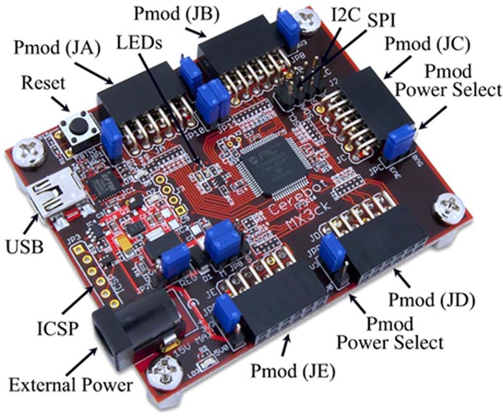
FIGURE 4.1 The chipKIT MX3 Development Board
A functional block diagram of the chipKIT MX3 development board is shown in Figure 4.2.
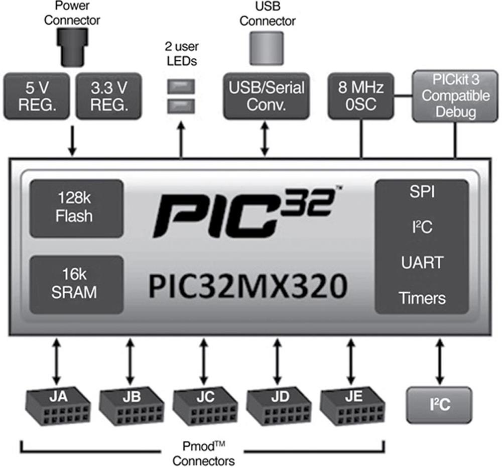
FIGURE 4.2 Functional Block Diagram of the chipKIT MX3 Development Board
4.1.1. Power Supply
Figure 4.3 shows a schematic of the power supply arrangement. The chipKIT MX3 can be powered either from USB port or from an external power supply. If both supplies are used, then the external supply is selected automatically. Two voltages are used on the board: +5 V (VCC5V0 bus) and +3.3 V (VCC3V3 bus).
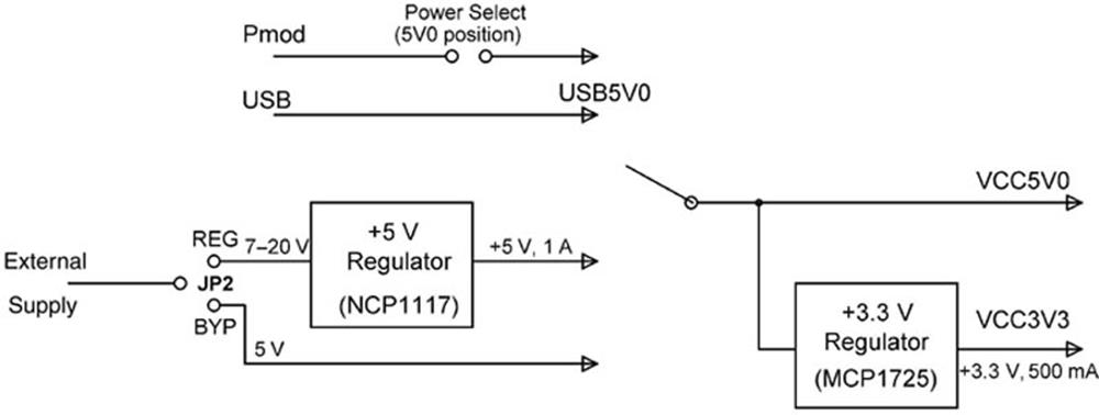
FIGURE 4.3 Schematic of the Power Supply Arrangement
External +5 V supply can be directly applied to the system by placing jumper JP2 in position BYP. Alternatively, 7–20 V external DC supply can be applied to the board with jumper JP2 in the REG position. In this configuration, the voltage regulator NCP1117 generates the required +5 V supply for the board, with the maximum current capacity of 1 A. The on-board +5 V supply is labelled as VCC5V0.
The +3.3 V supply is generated by the voltage regulator MCP1725, with the maximum current capacity of 500 mA. The input to this regulator must not exceed +6 V. The on-board +3.3 V supply is labelled as VCC3V3.
It is also possible to power the chipKIT MX3 from any of the Pmod connectors. This can be done by placing a Pmod power select jumper in the 5V0 position and applying +5 V through the connector. This will provide power to the VCC5V0 bus and also to the +3.3 V regulator.
The VCC3V3 bus can also be powered from the I2C connector or from a Pmod connector when the power select switch is in the +3.3 V position. In this configuration, only the VCC3V3 bus will be powered and the VCC5V0 bus will not be powered.
4.1.2. LEDs
There are two general-purpose user LEDs on the board, labelled LD4 and LD5. LD4 is connected to I/O port pin RF0, and LD5 is connected to I/O port pin RF1. Figure 4.4 shows the circuit diagram of the LEDs. The LEDs are turned on by driving them high. I/O pins RF0 and RF1 are dedicated to these LEDs and are not available at any connector.
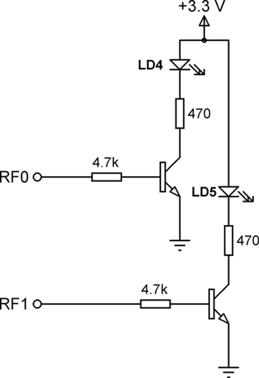
FIGURE 4.4 Circuit Diagram of the LEDs
4.1.3. Reset
A reset button (BTN1) is provided on the board that can be used to reset the microcontroller. The reset action is accomplished by lowering the MCLR pin of the microcontroller. Figure 4.5 shows the circuit diagram of the reset circuit.
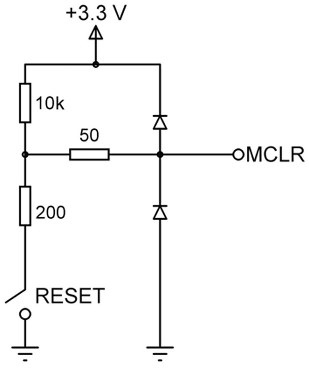
FIGURE 4.5 Reset Circuit
4.1.4. Pmod Connectors
The chipKIT MX3 has five connectors called Pmod (see Figure 4.1), labelled JA–JF for peripheral modules. These connectors have 12 pins organised in 2 rows as 2 × 16, and each connector has an associated power select jumper labelled JPA–JPF. The power select jumpers are used to select (between +5 and +3.3 V) the power supply voltage supplied to the power supply pin on the Pmod connector. Each connector provides eight I/O pins, two power pins, and two ground pins, organised as follows:
• Pins 1–4 and 7–10 are signal pins.
• Pins 5 and 11 are ground pins.
• Pins 6 and 12 are power pins.
The upper six pins are numbered 1–6 left to right as viewed from the top of the board. The lower six pins are numbered 7–12 left to right.
As shown in Figure 4.6, each Pmod pin is connected to a microcontroller I/O pin through a 200 Ω series resistor and a protection diode.
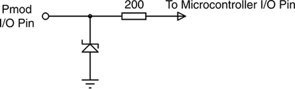
FIGURE 4.6 Pmod Pin Connections
The PIC32 microcontroller can source or sink up to 18 mA on its I/O pins. However, it is recommended to keep the source and sink currents to a maximum of 7 and 12 mA, respectively.
Tables 4.1–4.5 show the signal pin configurations of the Pmod connectors.
Table 4.1
JA connector signal pin configuration.
|
Pmod Connector |
I/O Pin |
|
JA1 |
RE0 |
|
JA2 |
RE1 |
|
JA3 |
RE2 |
|
JA4 |
RE3 |
|
JA7 |
RE4 |
|
JA8 |
RE5 |
|
JA9 |
RE6 |
|
JA10 |
RE7 |
Table 4.2
JB connector signal pin configuration.
|
Pmod Connector |
I/O Pin |
|
JB1 |
RD9 |
|
JB2 |
RF3 |
|
JB3 |
RF2 |
|
JB4 |
RF6 |
|
JB7 |
RD6 |
|
JB8 |
RD5 |
|
JB9 |
RD4 |
|
JB10 |
RD7 |
Table 4.3
JC connector signal pin configuration.
|
Pmod Connector |
I/O Pin |
|
JC1 |
RB8 |
|
JC2 |
RF5 |
|
JC3 |
RF4 |
|
JC4 |
RB14 |
|
JC7 |
RB0 |
|
JC8 |
RB1 |
|
JC9 |
RD0 |
|
JC10 |
RD1 |
Table 4.4
JD connector signal pin configuration.
|
Pmod Connector |
I/O Pin |
|
JD1 |
RB2 |
|
JD2 |
RD2 |
|
JD3 |
RD10 |
|
JD4 |
RB9 |
|
JD7 |
RB12 |
|
JD8 |
RD3 |
|
JD9 |
RD11 |
|
JD10 |
RB13 |
Table 4.5
JE connector signal pin configuration.
|
Pmod Connector |
I/O Pin |
|
JE1 |
RG9 |
|
JE2 |
RG8 |
|
JE3 |
RG7 |
|
JE4 |
RG6 |
|
JE7 |
RD8 |
|
JE8 |
RB5 |
|
JE9 |
RB4 |
|
JE10 |
RB3 |
4.1.5. CPU Clock
As shown in Figure 4.7, the microcontroller on the board is operated from an 8 MHz crystal. However, the internal phase-locked-loop (PLL) module of the microcontroller can be programmed to provide operating system clock (SYSCLK) frequency up to 80 MHz. The peripheral clock (PBCLK) frequency can be programmed as a division of the system clock frequency (factors of 1, 2, 4, or 8), and its maximum value can be 10 MHz.
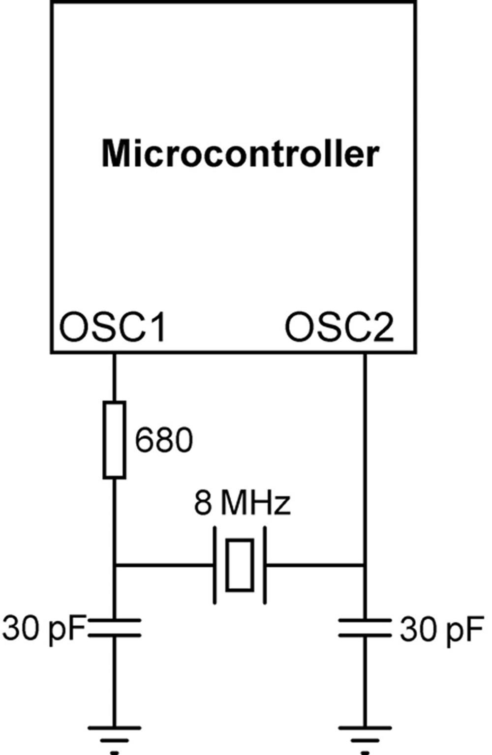
FIGURE 4.7 CPU Clock
4.1.6. I2C Bus Interface
The I2C bus on the board is an open-collector bus with medium speed communication, providing master and slave operation using either 7- or 10-bit device addressing. Although the PIC32MX320 microcontroller provides two I2C interfaces, the chipKIT MX3 is designed to provide only one interface (I2C1; the second I2C interface, I2C2, can be accessed at pins 2 and 3 of Pmod connector JC) on connector J2.
As shown in Figure 4.8, 2.2k resistors are used to pull up the SCL1 and SDA1 lines to the power supply (there are no pull-up resistors on the second I2C interface, I2C2).
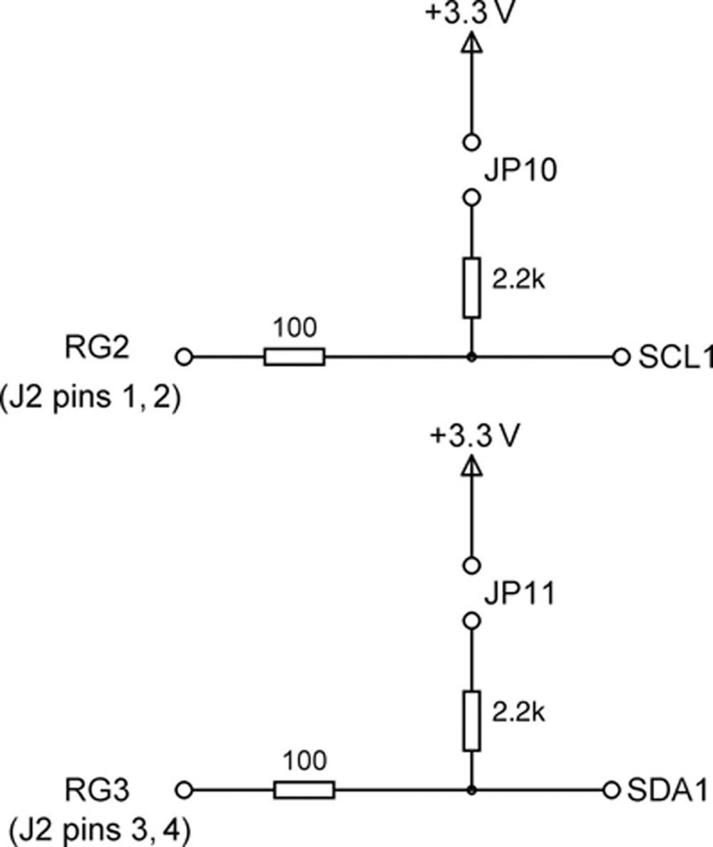
FIGURE 4.8 I2C Interface
4.1.7. SPI Bus Interface
The PIC32 microcontroller supports two SPI bus interfaces. Each interface has four signals, named SS (Slave Select), MOSI (Master Out Slave In), MISO (Master In Slave Out), and SCK (Serial Clock). SPI1 supports master mode only and is accessed via Pmod connector JB. SPI2 is accessed via Pmod connector JE:
JB-01: SS1
JB-02: MOSI1
JB-03: MISO1
JB-04: SCK1
JE-01: SS2
JE-02: MOSI2
JE-03: MISO2
JE-04: SCK2
As shown in Figure 4.9, jumpers JP6 and JP8 are used to select between master and slave for the SPI2 bus interface.
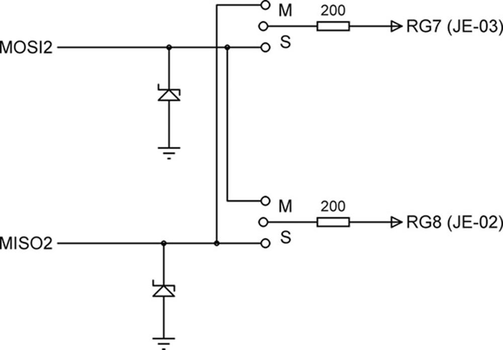
FIGURE 4.9 SPI Master/Slave Selection for SPI2
4.1.8. UART Interface
The PIC32MX320 microcontroller provides two UART interfaces, named UART1 and UART2. Either two-wire (TX and RX) or four-wire (RX, TX, RTS, CTS) communication is possible. UART1 and UART2 can be accessed from Pmod connectors JB and JC, respectively:
JB-01: UART1 (CTS)
JB-02: UART1 (TX)
JB-03: UART1 (RX)
JB-04: UART1 (RTS)
JC-01: UART2 (CTS)
JC-02: UART2 (TX)
JC-03: UART2 (RX)
JC-04: UART2 (RTS)
Figure 4.10 shows the UART1 schematic. Notice that the handshaking signals CTS, DSR, DCD, and RI are available on connector J3.
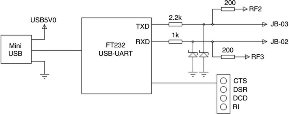
FIGURE 4.10 UART1 Schematic
4.1.9. Analogue Inputs
The chipKIT MX3 development board provides 11 analogue inputs (A0–A10). Interface to these analogue inputs is through Pmod connectors JC, JD, and JE:
A0: JC-01 (RB8)
A1: JC-04 (RB14)
A2: JC-07 (RB0)
A3: JC-08 (RB1)
A4: JD-01 (RB2)
A5: JD-04 (RB9)
A6: JD-07 (RB12)
A7: JD-10 (RB13)
A8: JE-08 (RB5)
A9: JE-09 (RB4)
A10: JE-10 (RB3)
The internal reference voltages for the analogue inputs can be selected as +3.3 V.
4.1.10. External Interrupts
PIC32 microcontroller supports five external interrupts named INT0–INT4. When using the MPIDE integrated development environment, these external interrupts are available in the following Pmod connectors:
INT0: JB-04, logical I/O port 11 (port pin RF6)
INT1: JE-07, logical I/O port 36 (port pin RD8)
INT2: JB-01, logical I/O port 8 (port pin RD9)
INT3: JD-03, logical I/O port 26 (port pin RD10)
INT4: JD-09, logical I/O port 39 (port pin RD11)
External interrupts are configured using the attachInterrupt(interrupt number, ISR, mode) function. The arguments of this function are as follows:
Interrupt number: The interrupt number is 0 (INT0) to 4 (INT4).
ISR: This is the interrupt service routine. This must be a function with no arguments, and no data can be returned from the interrupt service routine.
Mode: This parameter defines the interrupt mode. Valid modes are as follows:
|
LOW |
Interrupt triggered when the pin is LOW |
|
CHANGE |
Interrupt triggered when the pin changes value |
|
RISING |
Interrupt triggered when the pin state changes from LOW to HIGH |
|
FALLING |
Interrupt is triggered when the pin state changes from HIGH to LOW |
|
HIGH |
Interrupt is triggered when the pin is HIGH |
Function detachInterrupt(interrupt number) is used to turn off an interrupt.
4.1.11. Board Connectors and Jumpers
A list of the various connectors and jumpers on the chipKIT MX3 development board and the functions of these jumpers are given in Table 4.6.
Table 4.6
chipKIT MX3 board jumpers.
|
Jumpers |
Description |
|
JA–JE |
Pmod connectors |
|
JPA–JPE |
Pmod connector power select |
|
J1 |
Mini USB connector |
|
J2 |
I2C interface |
|
J3 |
Additional UART signals |
|
J4 |
External power connector |
|
JP1 |
Used to disconnect the USB from the MCLR reset input. Must be installed to use the board with the MPIDE development software |
|
JP2 |
External power select. If the jumper is in RTEG position, then external voltage is routed through the 5 V regulator |
|
JP3 |
Microchip development connector |
|
JP6, JP8 |
SPI2 master/slave select |
|
JP10, JP11 |
I2C pull-up resistor enable |
4.2. Pmod Peripheral Modules
Digilent offers a large number of Pmod-based peripheral devices in the form of small I/O interface boards for project development using their development boards. Pmod boards include sensors, data acquisition, simple I/O, LEDs, seven-segment displays, GPS, accelerometers, external memory, D/A converters, audio amplifiers, and many more.
Some of the popular Pmod modules are described briefly in this section. Detailed description of the Pmod modules can be found on the Digilent web site (www.digilentinc.com).
4.2.1. PmodSD – SD Card Slot
This is a small Secure Digital media card module (see Figure 4.11) that enables the programmer to use SD cards in projects.
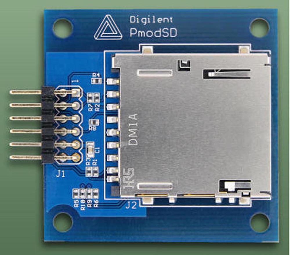
FIGURE 4.11 PmodSD
4.2.2. PmodCLP – Character LCD With Parallel Interface
This small board (see Figure 4.12) provides 2-line by 16-character (2 × 16) LCD interface to the development board.
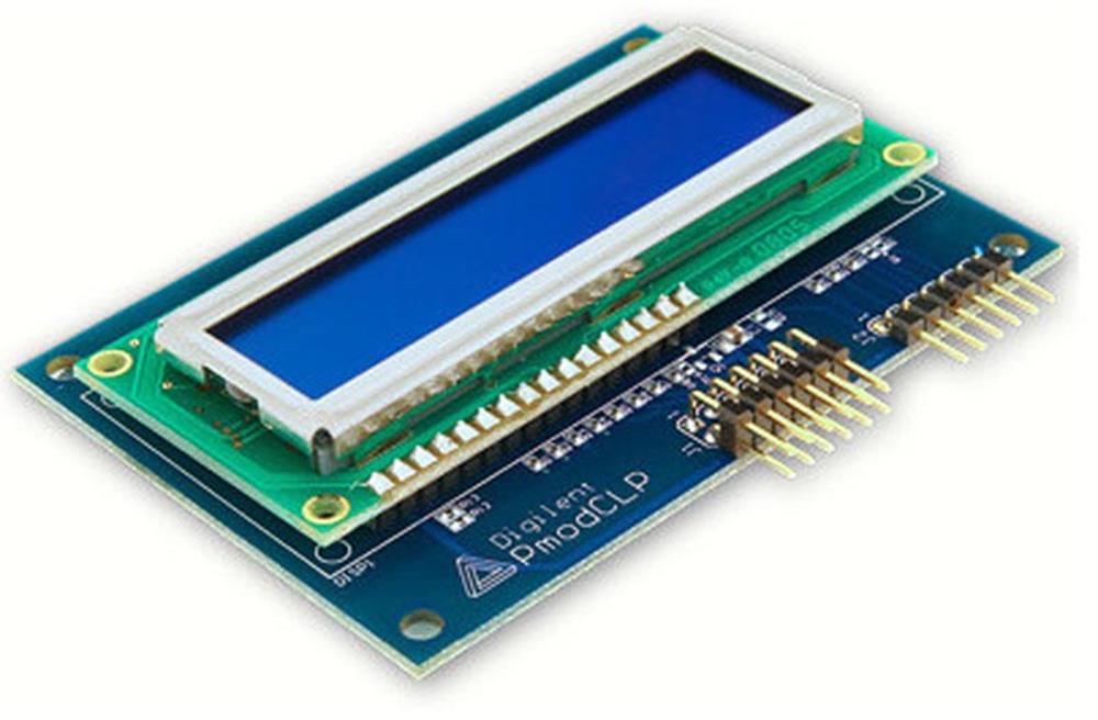
FIGURE 4.12 PmodCLP
4.2.3. PmodKYPD
This is a 16-key keypad (see Figure 4.13) with labelled buttons. Keypads are useful in projects where data entry may be required.
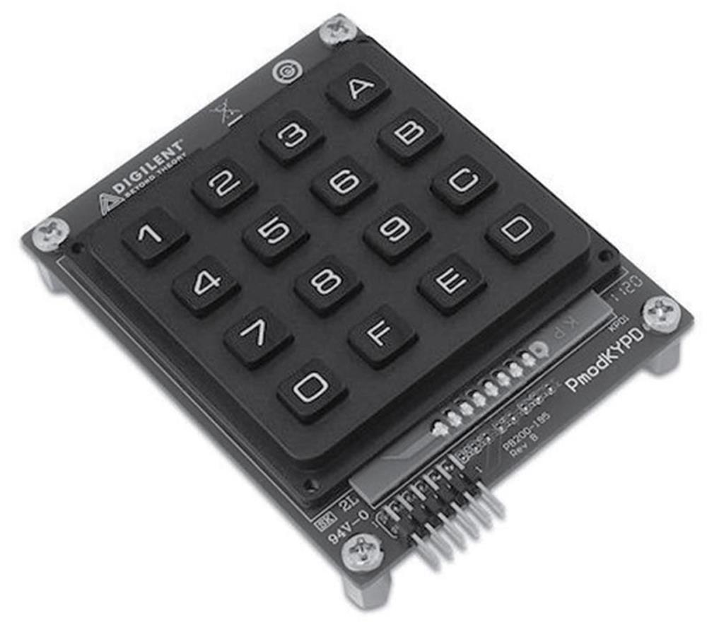
FIGURE 4.13 PmodKYPD
4.2.4. PmodSSD
This board provides two-digit seven-segment display (see Figure 4.14) to the development board.
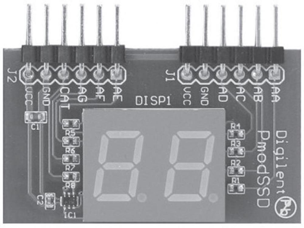
FIGURE 4.14 PmodSSD
4.2.5. PmodBTN
This is a small board with four debounced momentary push-button switches (see Figure 4.15).
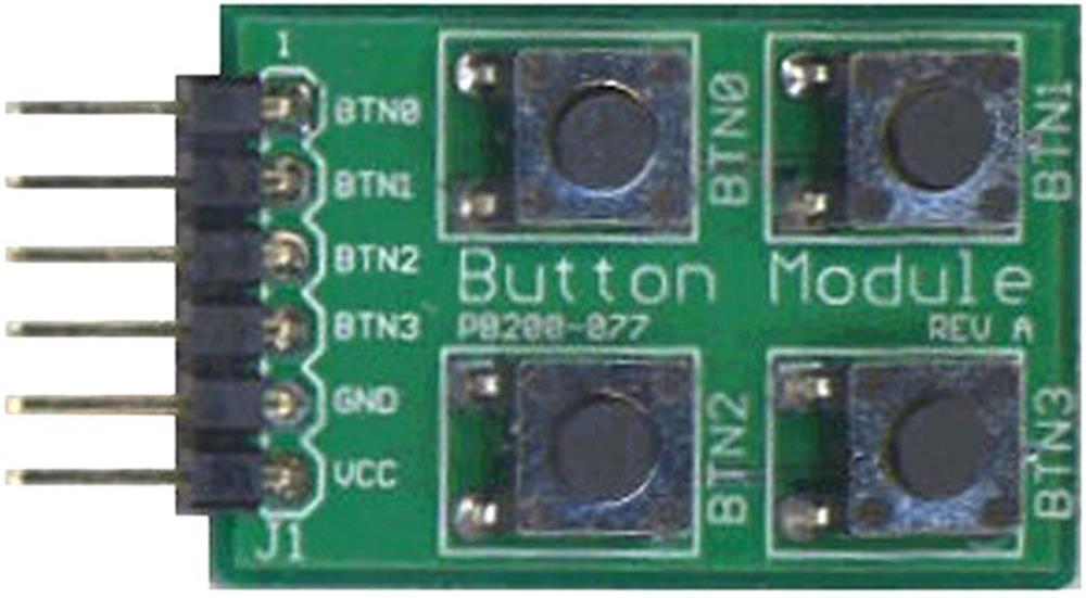
FIGURE 4.15 PmodBTN
4.2.6. PmodSTEP
This is a stepper motor controller board (see Figure 4.16) that can be used with four- and six-pin stepper motors.
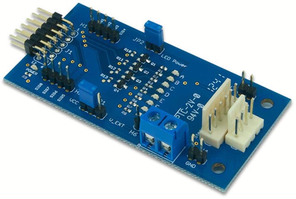
FIGURE 4.16 PmodSTEP
4.2.7. PmodTMP3
This is a programmable digital temperature sensor board with an accuracy of ±1°C (see Figure 4.17).
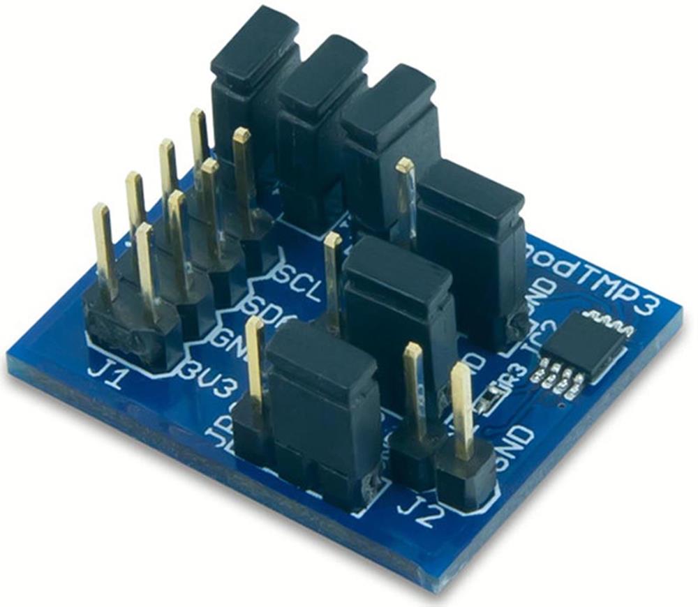
FIGURE 4.17 PmodTMP3
4.2.8. PmodDA1
This board incorporates four 8-bit D/A converters (see Figure 4.18).
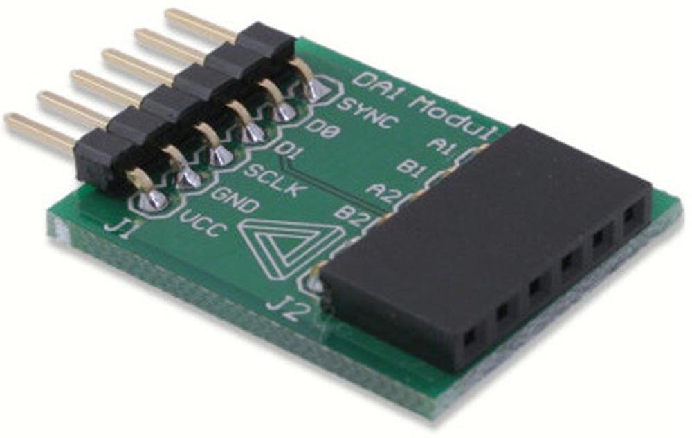
FIGURE 4.18 PmodDA1
4.2.9. PmodRTCC
This is a real-time clock/calendar board with lithium coin cell battery backup (see Figure 4.19).
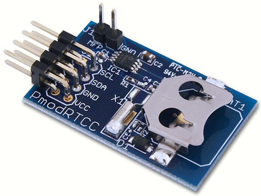
FIGURE 4.19 PmodRTCC
4.2.10. PmodBB
This board contains a wire wrap area and a small breadboard that can be used in projects (see Figure 4.20).
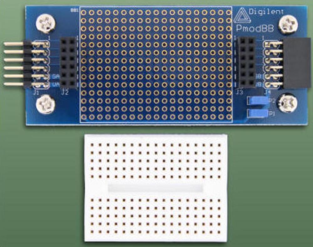
FIGURE 4.20 PmodBB
4.2.11. PmodAMP2
This is a small 2.5 W audio amplifier module (see Figure 4.21).
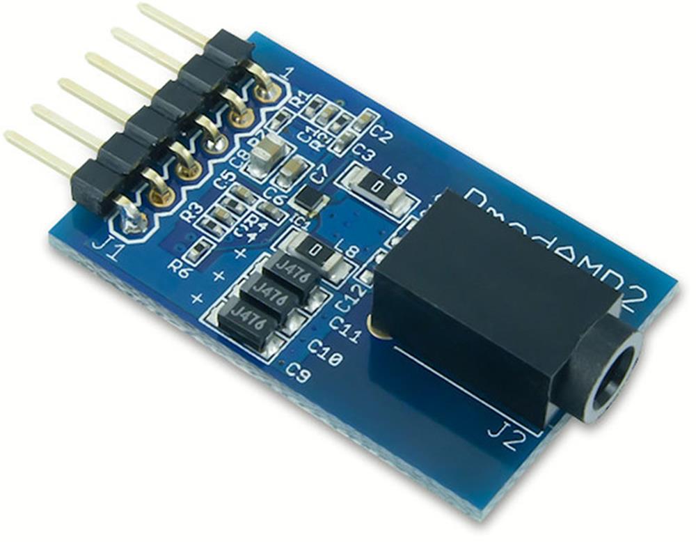
FIGURE 4.21 PmodAMP2
4.3. Summary
This chapter has explained the hardware details of the chipKIT MX3 development board. The functions and circuit diagrams of various components used on the board have been explained in the chapter. In addition, some of the popular Pmod peripheral modules have been described briefly.
All materials on the site are licensed Creative Commons Attribution-Sharealike 3.0 Unported CC BY-SA 3.0 & GNU Free Documentation License (GFDL)
If you are the copyright holder of any material contained on our site and intend to remove it, please contact our site administrator for approval.
© 2016-2026 All site design rights belong to S.Y.A.