PIC32 Microcontrollers and the Digilent chipKIT: Introductory to Advanced Projects (2015)
Chapter 7. Simple chipKIT MX3–Based Projects
Abstract
This chapter provides many tested and working microcontroller projects based on the PIC32 family of microcontrollers. The MPIDE development environment with the C language is used in all the projects. The following is given for each project: project title, project description, block diagram, circuit diagram, program description language, full program listing, and full description of the program. The projects cover topics such as LEDs, LCDs, seven-segment displays, sound projects, analogue-to-digital converter (ADC) projects, Global Positioning System (GPS) projects, temperature monitoring projects, stepper motor control projects, and many more.
Keywords
Microcontroller projects
MPIDE projects
chipKIT MX7 projects
C projects
PIC32 microcontroller projects
In this chapter, we shall be looking at the design of simple PIC32 32-bit microcontroller-based projects using the chipKIT MX3 development board and the MPIDE development environment, with the idea of becoming familiar with basic interfacing techniques and learning how to use the various microcontroller peripheral registers. We will look at the design of projects using LEDs, push-button switches, keyboards, LED arrays, sound devices, and so on. It is recommended that the reader move through the projects in their given order. The following are provided for each project:
• Description of the project
• Block diagram of the project
• Circuit diagram of the project
• Description of the hardware
• Algorithm description [in program description language (PDL)]
• Program listing
• Photos of the project (where applicable)
• Suggestions for further development (where applicable)
In this book, we will be using the PDL for all the projects.
The use of the MPIDE development environment will be discussed in detail in Project 7.1.
7.1. Project 7.1 – Flashing LED
7.1.1. Project Description
This is a simple project that flashes one of the LEDs on the chipKIT MX3 development board at a rate of once a second. There are two LEDs on the development board, and in this project the LED connected to I/O port pin RF0 (LED named LD4) is used. This LED has the logical pin number 42 (see Table 5.8).
An LED can be connected to a microcontroller output port in two different modes: current-sinking mode and current-sourcing mode.
7.1.2. Current-Sinking
As shown in Figure 7.1, in current-sinking mode the anode leg of the LED is connected to the Vdd supply, and the cathode leg is connected to the microcontroller output port through a current-limiting resistor.
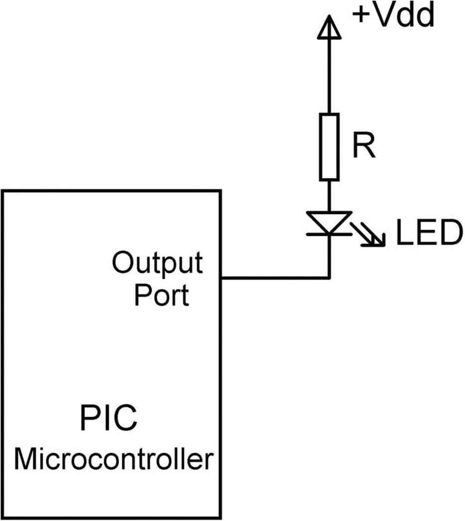
FIGURE 7.1 LED Connected in Current-Sinking Mode
The voltage drop across an LED is around 2 V. The brightness of the LED depends on the current through the LED, and this current can vary between a few milliamperes to 16 mA depending on the type of LED used.
The LED is turned ON when the output of the microcontroller is at logic 0 so that current flows through the LED. We can calculate the value of the required resistor as follows:

where Vdd is the supply voltage (3.3 V); VLED is the voltage drop across the LED (2 V); ILED is the current through the LED (say, 10 mA).
Substituting the values into the equation, we get

The nearest physical resistor is 120 Ω.
7.1.3. Current-Sourcing
As shown in Figure 7.2, in current-sourcing mode the anode leg of the LED is connected to the microcontroller output port and the cathode leg is connected to the ground through a current-limiting resistor.
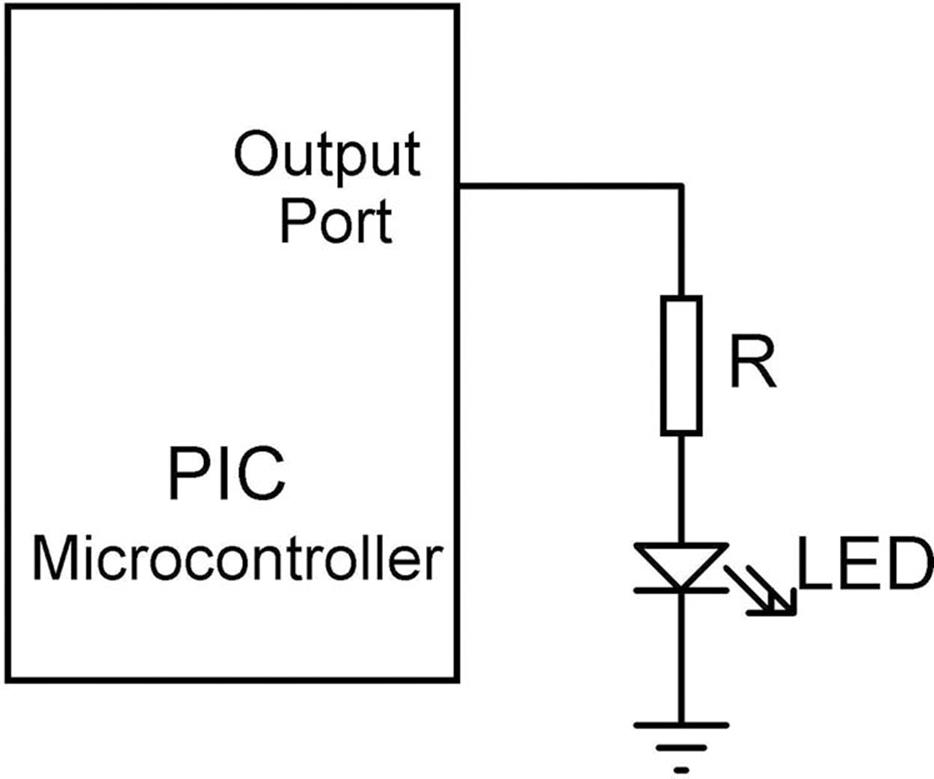
FIGURE 7.2 LED Connected in Current-Sourcing Mode
In this mode, the LED is turned ON when the microcontroller output port is at logic 1, that is, Vdd. In practice, the output voltage is about 3.3 V and the value of the resistor can be determined as:
which gives the same resistor value of 120 Ω.
7.1.4. Project Hardware
In this project, the LED named LD4 on the chipKIT MX3 development board is used. This LED is connected to port pin RF0 through a switching transistor as shown in Figure 4.4 (it is also possible to connect the LED through a current-limiting resistor as shown inFigures 7.1 and 7.2).
7.1.5. Project PDL
The operation of the project is described in the PDL given in Figure 7.3. At the beginning of the program, the LED port (logical port 42) is configured as output. The program then flashes the LED at a rate of 1 s by sending logic 1 and then logic 0 to the LED with 1-s delay between each output.
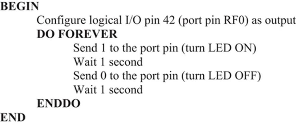
FIGURE 7.3 PDL of Project
7.1.6. Project Program
The program is called LED1, and the program listing is shown in Figure 7.4. At the beginning of the program, the port pin where LD4 is connected to is configured as an output inside the setup() function. The LED is then flashed ON and OFF by sending 1 and 0 continuously with 1-s delay between each output.
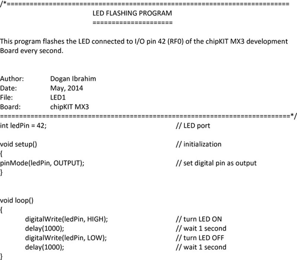
FIGURE 7.4 Program Listing
The following steps describe how to create the program and upload it to the flash memory of the target microcontroller on the chipKIT MX3 development board:
Step 1: Start the MPIDE development environment.
Step 2: Enter the program shown in Figure 7.4 (see Figure 7.5).
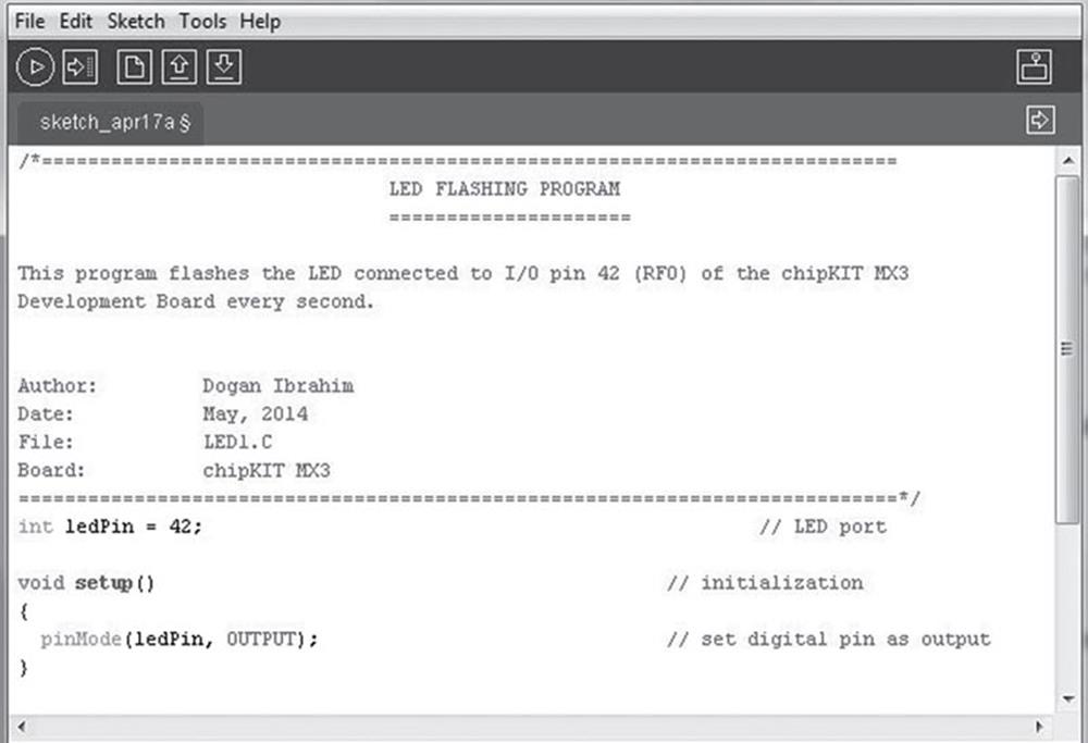
FIGURE 7.5 Enter the Program Using the MPIDE Development Environment
Step 3: Select the development board type by clicking Tools → Board → Cerebot → Mx3cK.
Step 4: Compile the program by clicking the Verify button in the toolbar. If the program compiles successfully, you should get no error messages (see Figure 7.6).
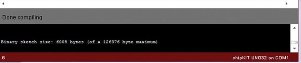
FIGURE 7.6 Program Compiled With No Errors
Step 5: Connect the chipKIT MX3 development board to the USB port of your computer. You should see the red power LED coming on and the green BootLoader LED (LD4) flashing rapidly.
Step 6: Select the serial COM port number assigned to the board. This number can be found from Control Panel → System → Device Manager under the heading Ports (COM & LPT) → USB Serial Port (see Figure 7.7).
Click Tools → Serial Port to select or confirm the assigned port as shown in Figure 7.8.
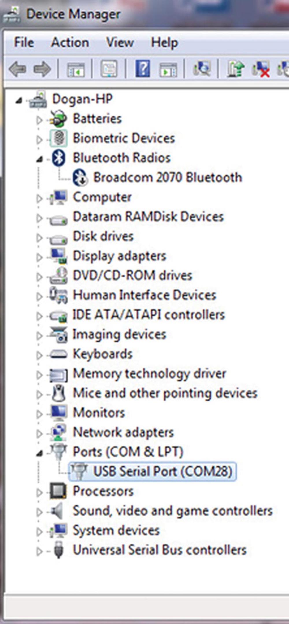
FIGURE 7.7 The Assigned COM Port Is COM28
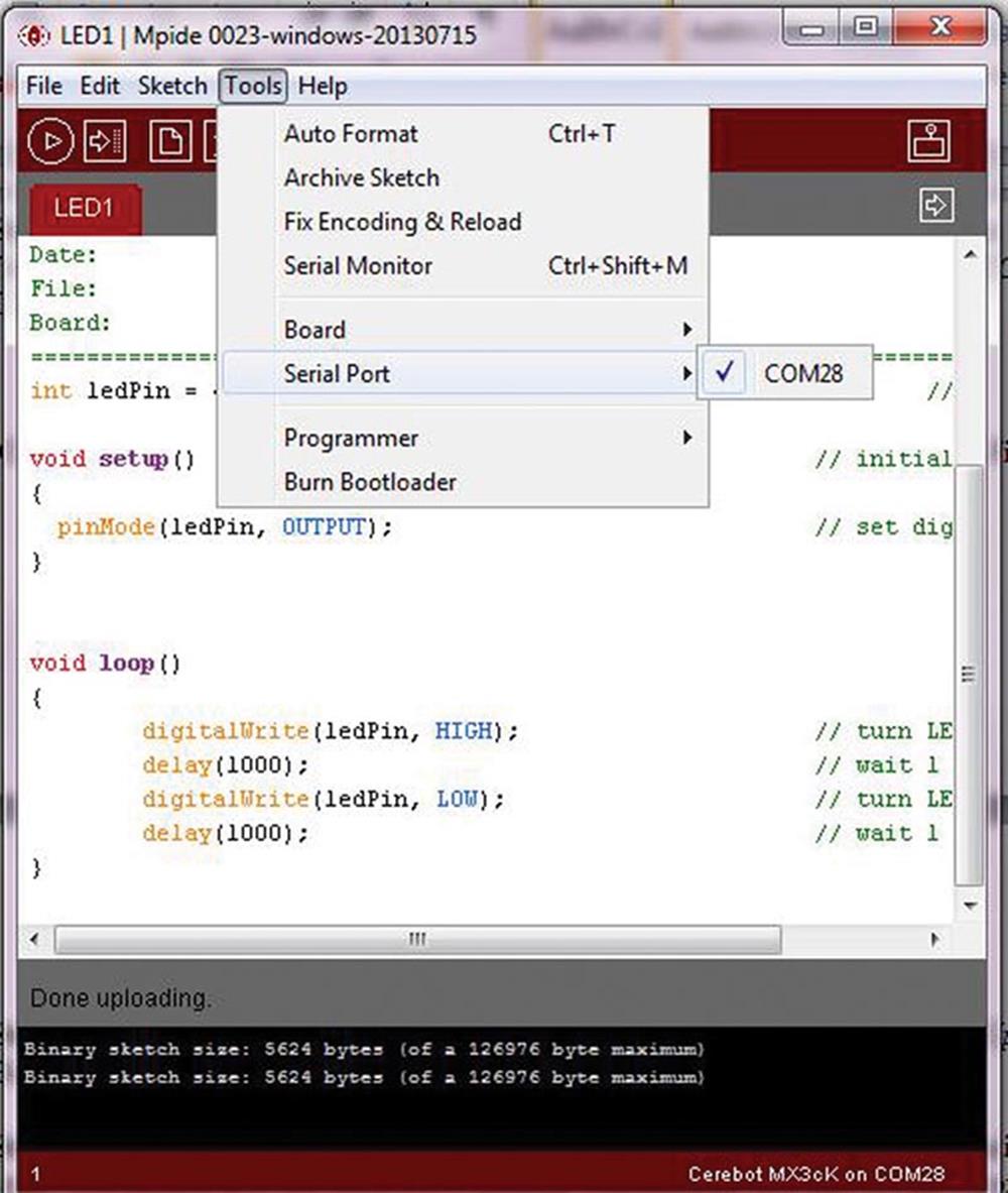
FIGURE 7.8 Select/Confirm the Assigned COM Port
Step 7: Upload the program to the target microcontroller by clicking File → Upload to I/O Board. You should see the message Done uploading as in Figure 7.9.
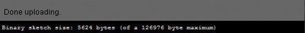
FIGURE 7.9 Successful Uploading of the Program
Step 8: The microcontroller should reset automatically and the program execution should start. You should now see LED LD4 flashing continuously at a rate of 1 s.
Notice that after pressing the Reset button, the green LED flashes rapidly and the microcontroller waits for about 10 s to communicate with the MPIDE programmer. If there is no response from the programmer, then execution of the user program starts.
7.2. Project 7.2 – Alternately Flashing LEDs
7.2.1. Project Description
This is a simple project similar to Project 7.1. Here, two LEDs flash alternately with 1-s delay between each output. The two LEDs LD4 (I/O port pin RF0, logical pin number 42) and LD5 (I/O port pin RF1, logical pin number 43) on the chipKIT MX3 development board are used in this project. See Table 5.8 for I/O pin assignments.
7.2.2. Project Hardware
Figure 4.4 shows how the LEDs LD4 and LD5 are connected on the chipKIT MX3 development board through switching transistors (it is also possible to connect the LEDs through current-limiting resistors as shown in Figures 7.1 and 7.2).
7.2.3. Project PDL
The operation of the project is described in the PDL given in Figure 7.10. At the beginning of the program, LD4 (logical port 42) and LD5 (logical port 43) are configured as outputs. The program then flashes the two LEDs alternately at a rate of 1 s by sending logic 1 and then logic 0 to the LEDs alternately with 1-s delay between each output.
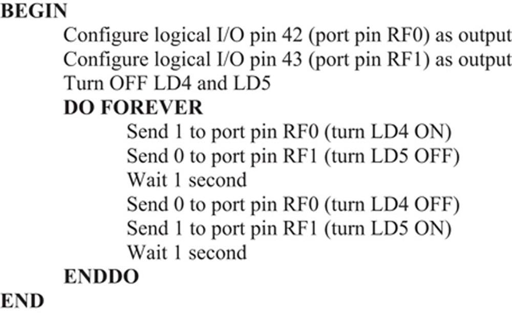
FIGURE 7.10 PDL of Project
7.2.4. Project Program
The program is called LED2, and the program listing is shown in Figure 7.11. At the beginning of the program, the port pins where LD4 and LD5 are connected to are configured as outputs inside the setup() function. Also, both LEDs are turned OFF to start with. The LEDs are then flashed ON and OFF alternately by sending 1 and 0 continuously with 1-s delay between each output.
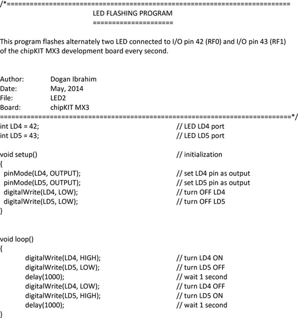
FIGURE 7.11 Program Listing
7.3. Project 7.3 – Lighthouse Flashing LED
7.3.1. Project Description
This is a simple project using LED LD4. In this project, the LED is flashed in a group of two quick flashes every second. The flashing rate is assumed to be 200 ms. This type of flashing is identified as Gp Fl(2) in maritime lighthouse lights. Thus, the flashing is repeated as follows:
LED ON
Wait 200 ms
LED OFF
Wait 100 ms
LED ON
Wait 200 ms
LED OFF
Wait 100 ms
Wait 400 ms
7.3.2. Project Hardware
Figure 4.4 shows how LD4 is connected on the chipKIT MX3 development board through a switching transistor (it is also possible to connect the LEDs through current-limiting resistors as shown in Figures 7.1 and 7.2).
7.3.3. Project PDL
The operation of the project is described in the PDL given in Figure 7.12. At the beginning of the program, LD4 (logical port 42) is configured as an output. The program then flashes the LED as a lighthouse signal Gp Fl(2) as described above.
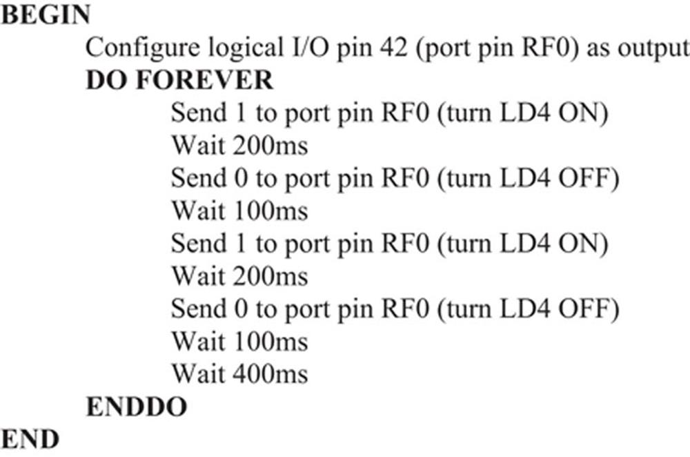
FIGURE 7.12 PDL of Project
7.3.4. Project Program
The program is called LED3, and the program listing is shown in Figure 7.13. At the beginning of the program, the port pin where LD4 is connected to is configured as an output inside the setup() function. The LED is then flashed ON and OFF to simulate the lighthouse signalling Gp Fl(2) as described above.
FIGURE 7.13 Program Listing
7.4. Project 7.4 – LED With Push-Button Switch
7.4.1. Project Description
This is a simple project using LED LD4 with a push-button switch. In this project, the LED is controlled from a push-button switch and is turned ON and OFF when the switch is pushed and released, respectively.
7.4.2. Block Diagram
The block diagram of the project is shown in Figure 7.14.
FIGURE 7.14 Block Diagram of the Project
7.4.3. Project Hardware
In this project, the four-button Pmod module PmodBTN is used (see Figure 7.15). This module consists of four push-button switches labelled BTN0–BTN3 with on-board debounce filters as shown in Figure 7.16.
FIGURE 7.15 PmodBTN Module
FIGURE 7.16 PmodBTN Module Connection Diagram
The PmodBTN module has a six-pin header and is connected to Pmod connector JA on the chipKIT MX3 development board.
The pin connections of the PmodBTN module are as follows:
|
Pin Number |
Pin Function |
|
1 |
BTN0 |
|
2 |
BTN1 |
|
3 |
BTN2 |
|
4 |
BTN3 |
|
5 |
GND |
|
6 |
VCC |
A switch pin is at logic 0 and goes to logic 1 when the switch is pressed. When connected to Pmod connector JA, the interface between the switch and the microcontroller I/O pins when the PmodBTN is connected to the top row of the connector is as follows:
|
Pin Number |
Microcontroller I/O Port Pin |
|
1 |
RE0 (JA-01, logical I/O pin 0) |
|
2 |
RE1 (JA-02, logical I/O pin 1) |
|
3 |
RE2 (JA-03, logical I/O pin 2) |
|
4 |
RE3 (JA-04, logical I/O pin 3) |
In this project, BTN0 is used. This switch has the logical I/O pin number 0 as shown in the above table.
Figure 7.17 shows the PmodBTN module connected to the development board.
FIGURE 7.17 Connecting the PmodBTN Module to the Development Board
7.4.4. Project PDL
The operation of the project is described in the PDL given in Figure 7.18. At the beginning of the program, LD4 (logical port 42) is configured as an output and connector JA-01 pin (logical port 0) is configured as an input. The LED is turned ON when the push-button switch is pressed, that is, when the ButtonState is at logic 1.
FIGURE 7.18 PDL of Project
7.4.5. Project Program
The program is called PUSH1, and the program listing is shown in Figure 7.19. At the beginning of the program, the port pin where LED LD4 is connected to is configured as an output and the port pin where button BTN0 is connected to is configured as an input inside the setup() function. The program then reads the state of the button, and the LED is turned ON whenever the button is pressed; otherwise, the LED is turned OFF.
FIGURE 7.19 Program Listing of Project
7.5. Project 7.5 – Wait Before Flashing the LED
7.5.1. Project Description
This is a simple project similar to Project 7.4. Here, LED LD4 and push-button BTN0 are used as in Project 7.4. THE LED is normally OFF and starts flashing at a rate of 1 s when the push-button switch is pressed.
7.5.2. Block Diagram
The block diagram of the project is as in Figure 7.14.
7.5.3. Project Hardware
The project hardware is as in Project 7.4 where a PmodBTN module is used. This module consists of four push-button switches labelled BTN0–BTN3 with on-board debounce filters, and BTN0 is used in this project. The PmodBTN module is connected to Pmod connector JA, and thus BTN0 has the logical I/O pin number 0 as in the previous project.
7.5.4. Project PDL
The operation of the project is described in the PDL given in Figure 7.20. At the beginning of the program, LD4 (logical port 42) is configured as an output and connector JA-01 pin (logical port 0) is configured as an input. The LED is normally OFF and starts flashing at a rate of 1 s as soon as the switch is pressed.
FIGURE 7.20 PDL of Project
7.5.5. Project Program
The program is called PUSH2, and the program listing is shown in Figure 7.21. At the beginning of the program, the port pin where LED LD4 is connected to is configured as an output and the port pin where button BTN0 is connected to is configured as an input inside the setup() function. The program then reads the state of the button in a loop and waits until the button is pressed. As soon as the button is pressed, the LED starts flashing at a rate of 1 s.
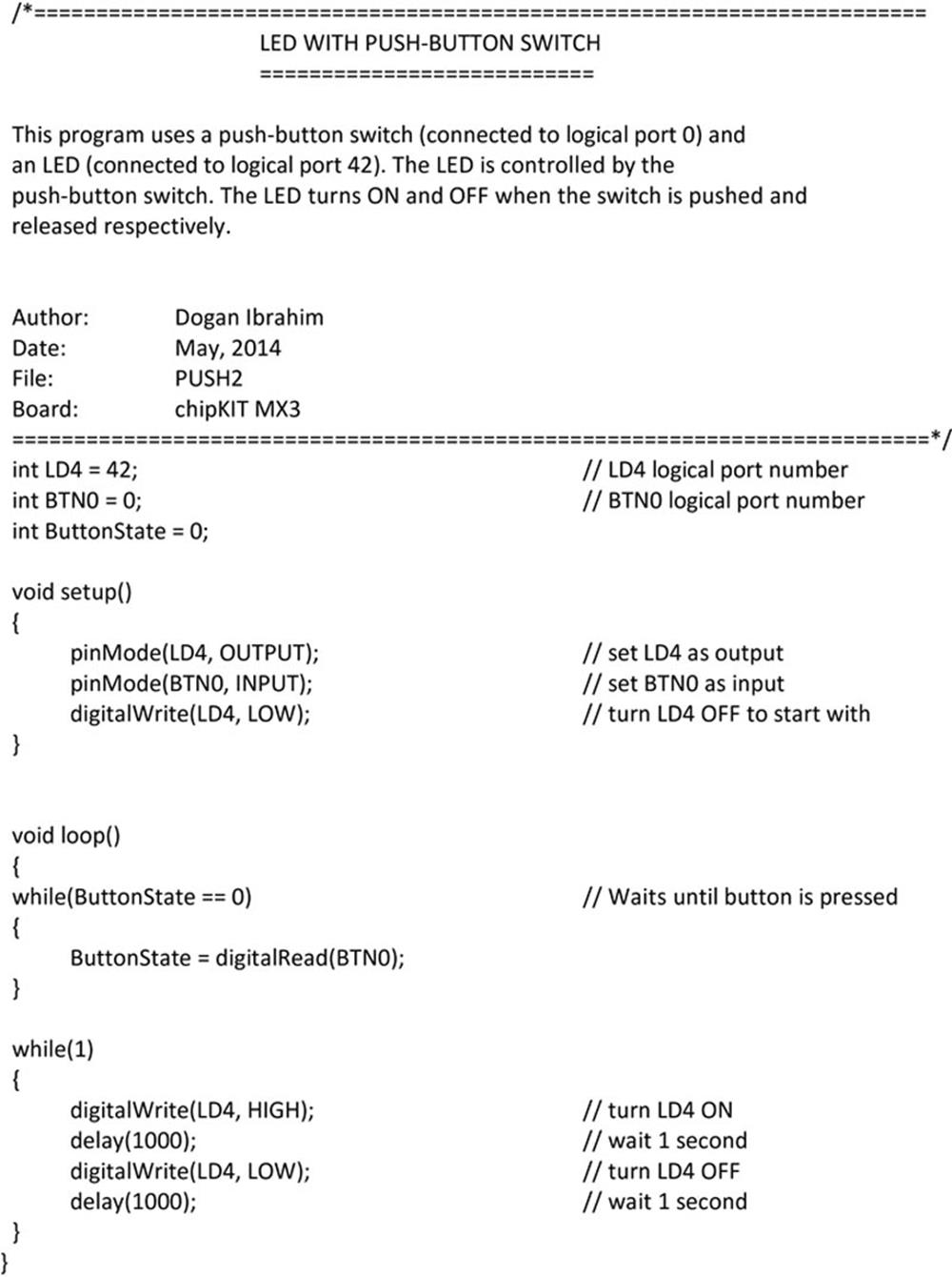
FIGURE 7.21 Program Listing of the Project
7.6. Project 7.6 – LED With Two Push-Button Switches
7.6.1. Project Description
This is a simple project similar to Project 7.4. Here, LED LD4 and two push-button switches BTN0 and BTN1 are used. The LED is normally OFF and starts flashing at a rate of 500 ms when the push-button switch BTN0 is pressed. The LED stops flashing when push-button BTN1 is pressed.
7.6.2. Block Diagram
The block diagram of the project is shown in Figure 7.22.
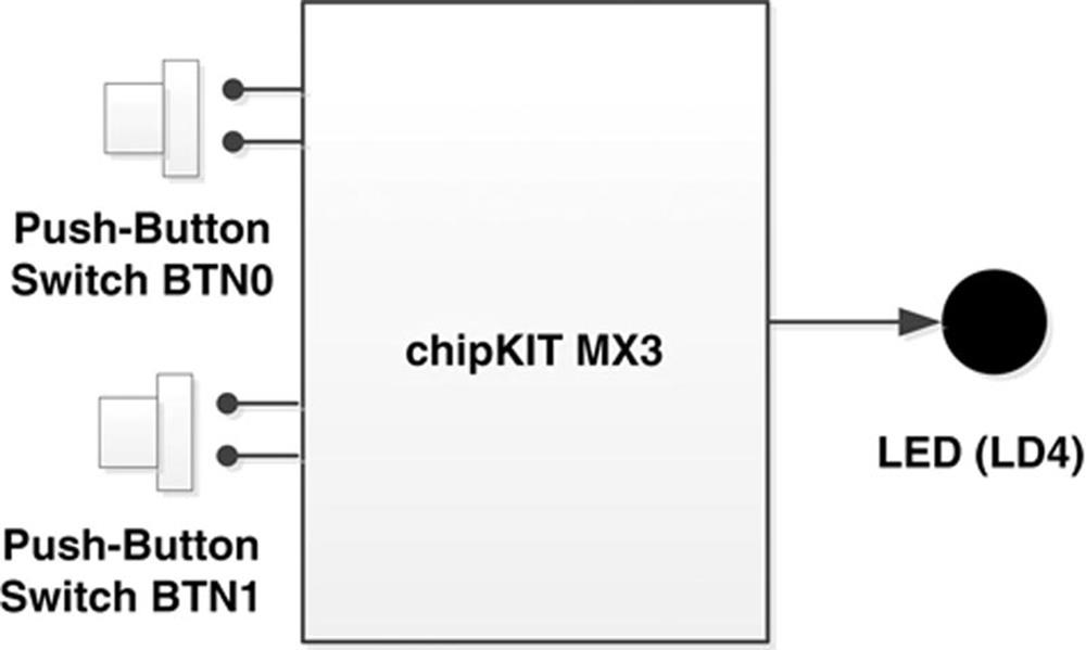
FIGURE 7.22 Block Diagram of the Project
7.6.3. Project Hardware
The project hardware is similar to Project 7.4 where a PmodBTN module is used. This module consists of four push-button switches labelled BTN0–BTN3 with on-board debounce filters. BTN0 is used to start flashing the LED, and BTN1 is used to stop flashing the LED. The PmodBTN module is connected to Pmod connector JA. BTN0 (connector pin JA-01) and BTN1 (connector pin JA-02) have the logical I/O pin numbers 0 and 1, respectively (see Project 7.4).
7.6.4. Project PDL
The operation of the project is described in the PDL shown in Figure 7.23. At the beginning of the program, LD4 (logical port 42) is configured as an output and connector JA-01 pin (BTN0, logical port 0) and JA-02 pin (BTN1, logical port 1) are configured as inputs. The LED is turned ON when the push-button switch BTN0 is pressed. The LED is turned OFF when push-button switch BTN1 is pressed.
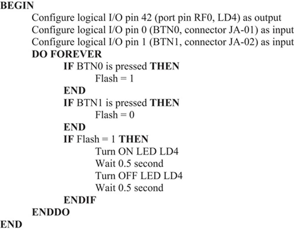
FIGURE 7.23 PDL of the Project
7.6.5. Project Program
The program is called PUSH2, and the program listing is shown in Figure 7.24. At the beginning of the program, the port pin where LED LD4 is connected to is configured as an output and the port pins where buttons BTN0 and BTN1 are connected to are configured as inputs inside the setup() function. The program then reads the state of both buttons. If BTN0 is pressed, then variable Flash is set to 1. If, on the other hand, BTN1 is pressed, then variable Flash is cleared to zero. The LED starts flashing at a rate of 500 ms if variable Flash is set to 1. The flashing stops when variable Flash is cleared.
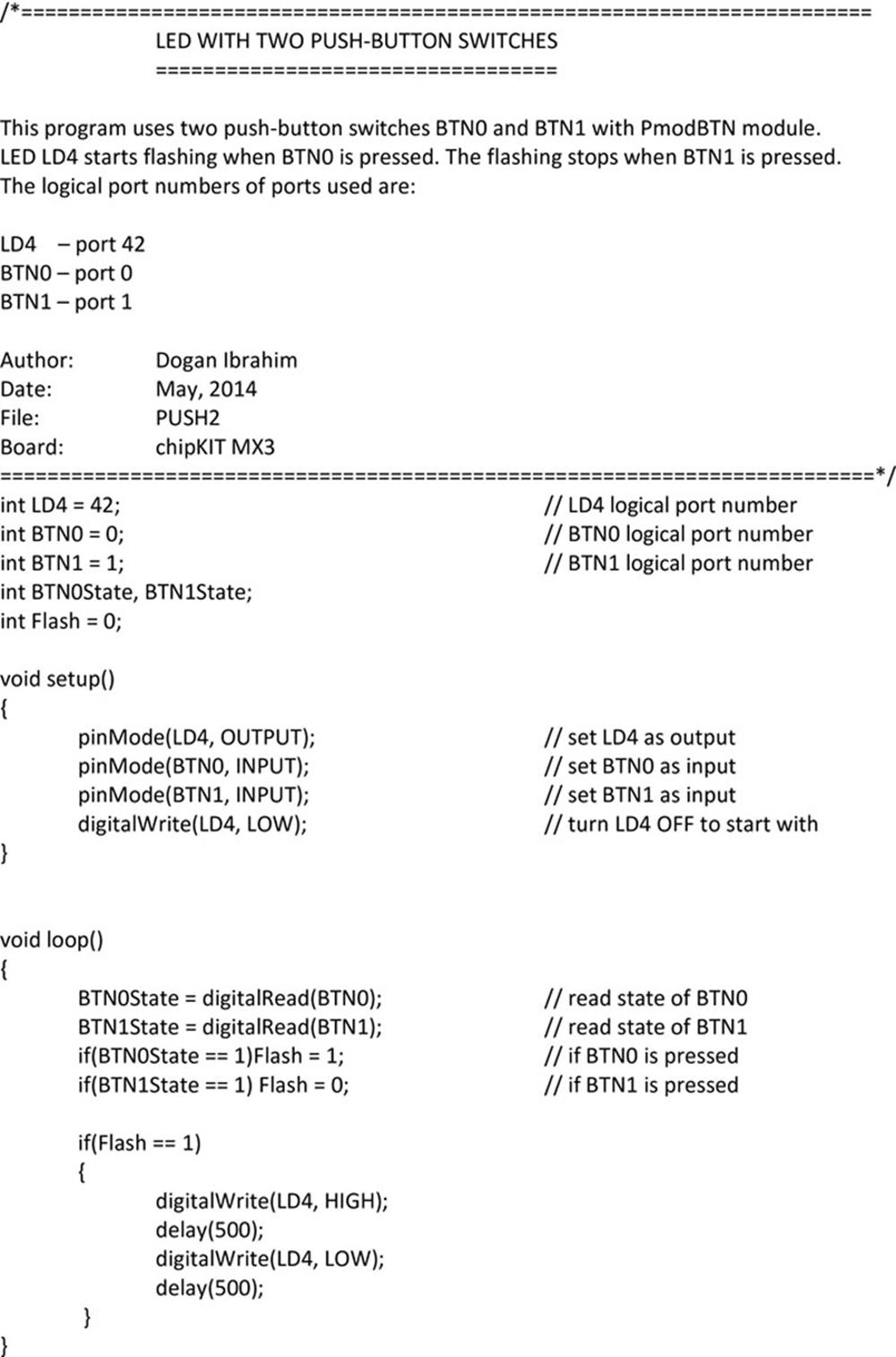
FIGURE 7.24 Program Listing of the Project
7.7. Project 7.7 – Rotating LEDs
7.7.1. Project Description
In this project, four LEDs are used and these LEDs are turned ON in a rotating manner, that is, the ON/OFF pattern of the LEDs is as follows:
7.7.2. Block Diagram
The block diagram of the project is shown in Figure 7.25.
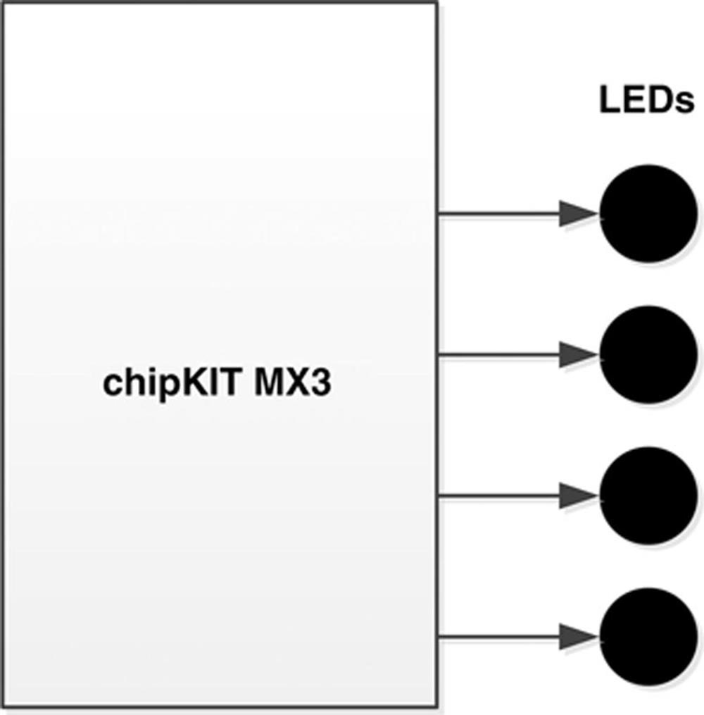
FIGURE 7.25 Block Diagram of the Project
7.7.3. Project Hardware
In this project, the PmodLED module is used. This is a small Pmod module with four LEDs as shown in Figure 7.26. The connection diagram of this module is shown in Figure 7.27. Each LED is driven from a transistor circuit with a minimum of 1 mA current.
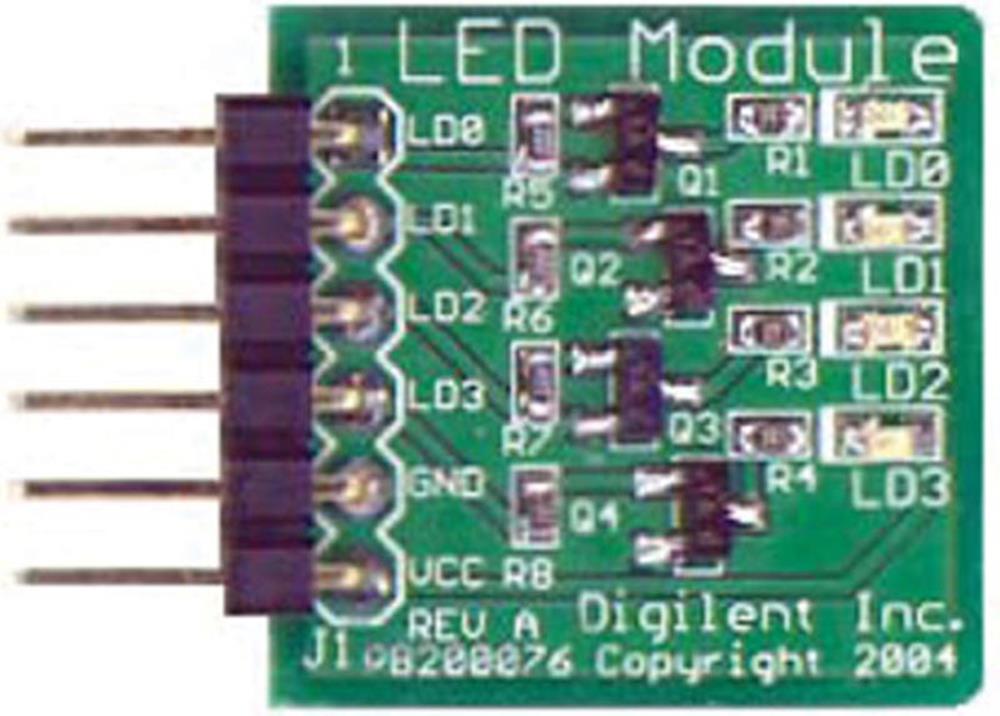
FIGURE 7.26 The PmodLED Module
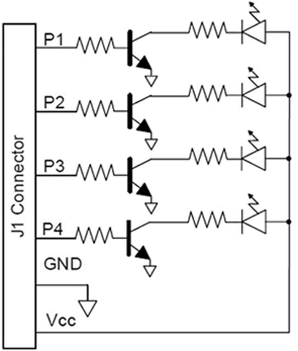
FIGURE 7.27 Connection Diagram of the PmodLED Module
The pin connections of the PmodLED module are as follows:
|
Pin Number |
Pin Function |
|
1 |
LD0 |
|
2 |
LD1 |
|
3 |
LD2 |
|
4 |
LD3 |
|
5 |
GND |
|
6 |
VCC |
When connected to Pmod connector JA, the interface between the module and the microcontroller I/O pins when the PmodLED is connected to the top row of the connector is as follows:
|
Pin Number |
Microcontroller I/O Port Pin |
|
1 |
RE0 (JA-01, logical I/O pin 0) |
|
2 |
RE1 (JA-02, logical I/O pin 1) |
|
3 |
RE2 (JA-03, logical I/O pin 2) |
|
4 |
RE3 (JA-04, logical I/O pin 3) |
Figure 7.28 shows the PmodLED module connected to the development board. The LEDs are configured as follows:

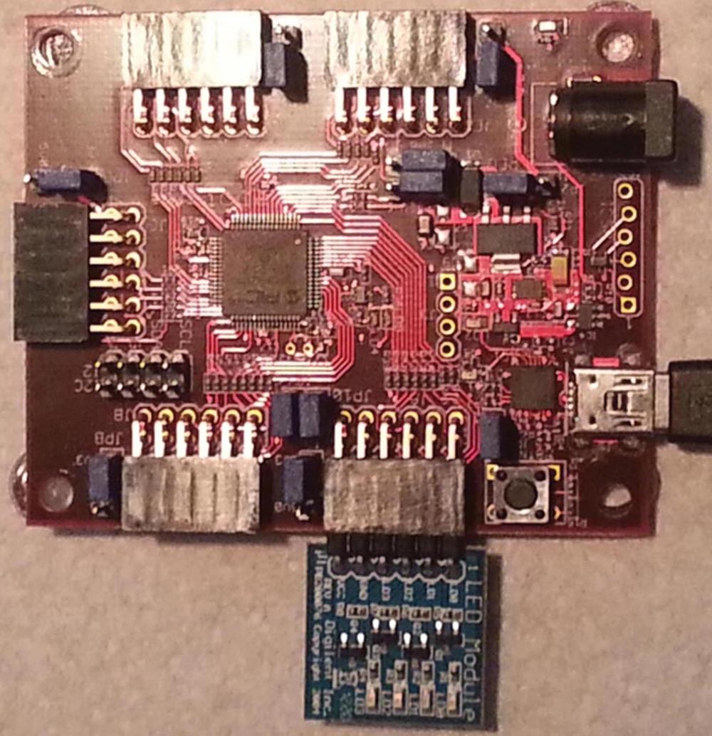
FIGURE 7.28 Connecting the PmodLED Module to the Development Board
7.7.4. Project PDL
The operation of the project is described in the PDL given in Figure 7.29. At the beginning of the program, LD1–LD4 (logical ports 0–3) are configured as outputs. The LEDs are turned ON and OFF in a rotating manner.
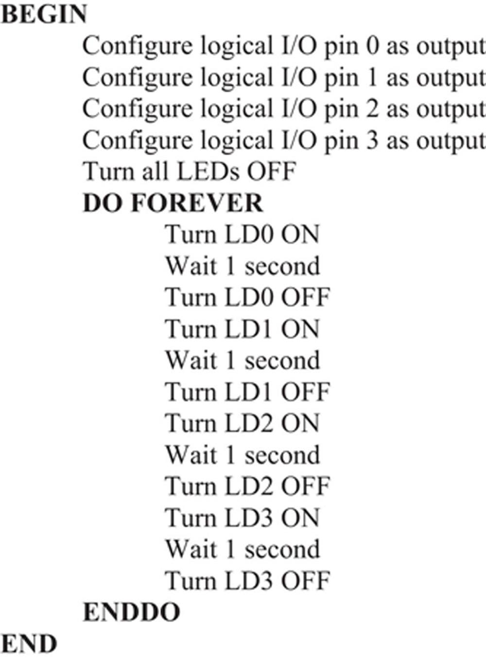
FIGURE 7.29 PDL of the Project
7.7.5. Project Program
The program is called ROTATE1, and the program listing is shown in Figure 7.30. At the beginning of the program, logical ports 0–3 corresponding to LEDs LD0–LD3 are configured as outputs and all the LEDs are turned OFF. Then, the LEDs are turned ON one at a time in a rotating manner with 1-s delay between each output.
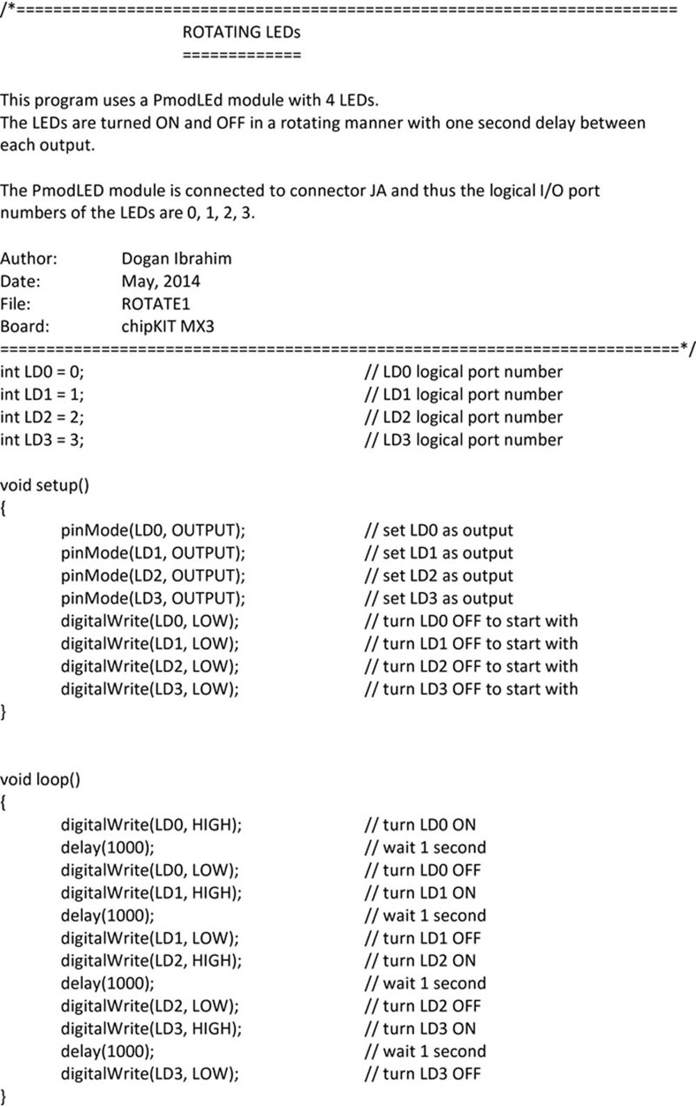
FIGURE 7.30 Program Listing of the Project
7.7.6. Modified Program
The program given in Figure 7.30 can be modified and made more efficient by using an array to store the port I/O logical port numbers. The modified program is called ROTATE2 and is shown in Figure 7.31. In this version of the program, integer array PmodLED is loaded with the logical port I/O numbers. These ports are then configured as outputs inside the setup() function. Inside the main program, a loop is formed to send data to the LEDs in a rotating manner.
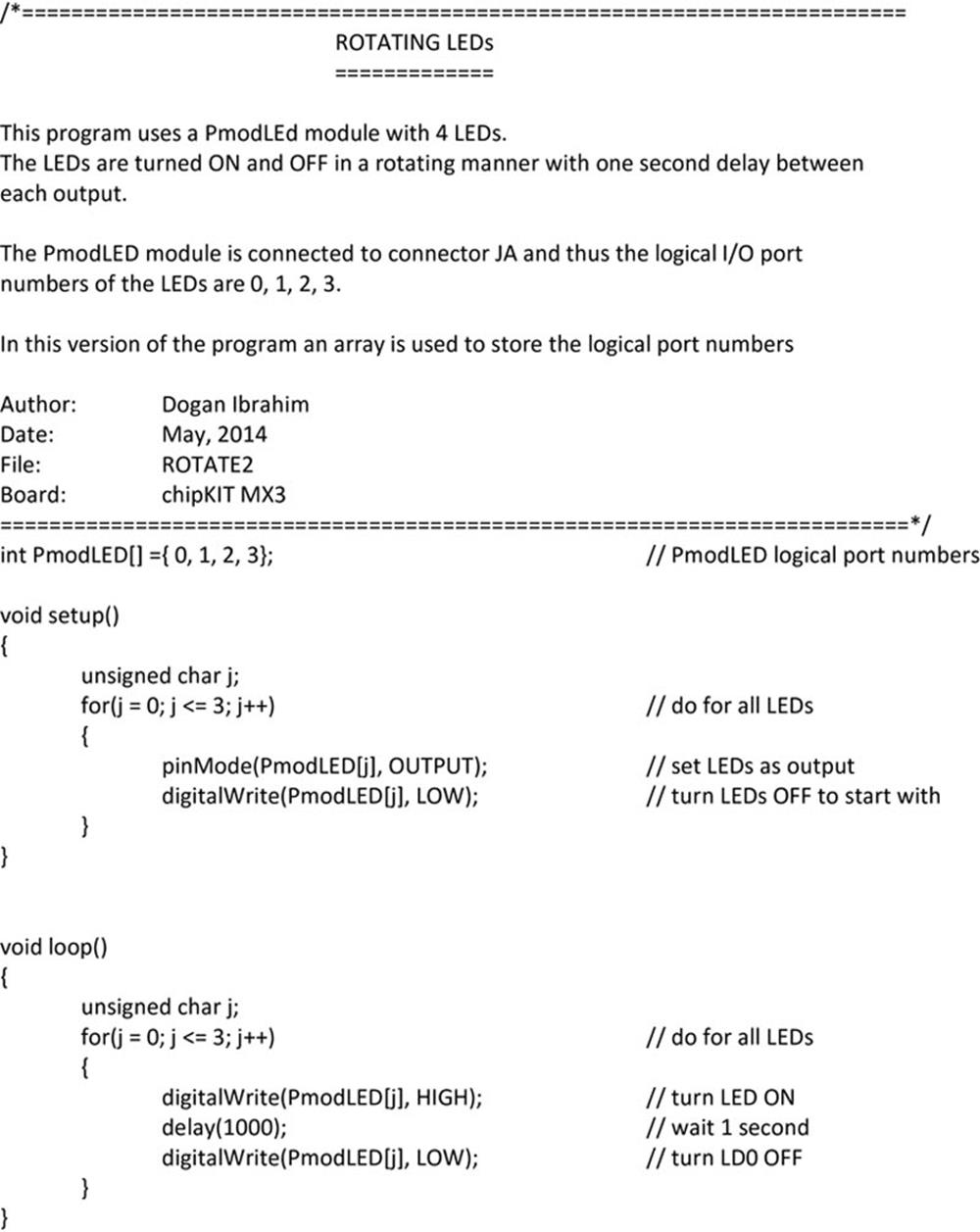
FIGURE 7.31 Modified Program
7.7.7. Another Version of the Program
Another version of the program is given in this section where data is sent to PORTE where the LEDs are connected to in order to turn the LEDs ON and OFF. This version of the program is called ROTATE3 and is shown in Figure 7.32. PORTE is configured as output by clearing the TRISE register. Then, a variable called j is used in the main program loop to turn the LEDs ON and OFF. This variable takes the values of 1, 2, 4, 8, 1, 2, ….
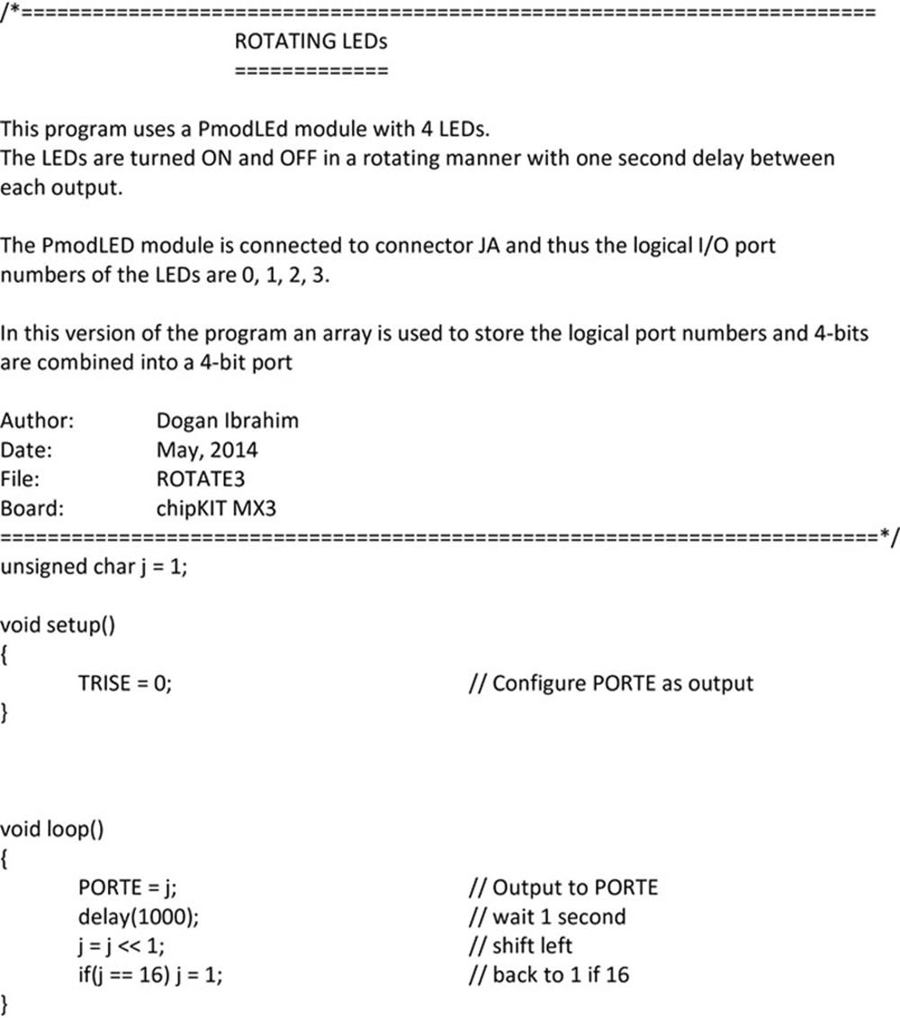
FIGURE 7.32 Another Version of the Program
7.8. Project 7.8 – Random Flashing LEDs
7.8.1. Project Description
In this project, four LEDs are used as in Project 7.7 and these LEDs are turned ON and OFF randomly with 1-s delay between each output.
7.8.2. Block Diagram
The block diagram of the project is as in Figure 7.25.
7.8.3. Project Hardware
In this project, the PmodLED module is used as in Project 7.7 and is connected to Pmod connector JA, that is, the four LEDs are connected to PORTE low nibble.
7.8.4. Project PDL
The operation of the project is described in the PDL given in Figure 7.33. At the beginning of the program, PORTE is configured as output. Then, inside the main program loop, a random number is generated between 1 and 15, and this number is sent to PORTE to turn the LEDs ON and OFF accordingly.
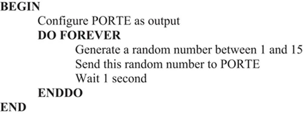
FIGURE 7.33 PDL of the Project
7.8.5. Project Program
The program is called RANDOM, and the program listing is shown in Figure 7.34. At the beginning of the program, register TRISE is cleared to make PORTE pins outputs. Then, inside the main program, a random number is generated between 1 and 15 using the built-in random function, and this number is sent to PORTE. This process is repeated continuously after 1-s delay.
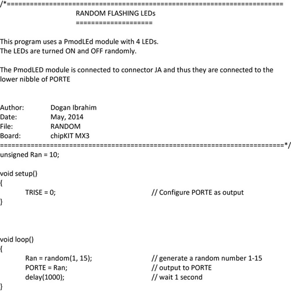
FIGURE 7.34 Program Listing of the Project
7.9. Project 7.9 – Fading LED
7.9.1. Project Description
In this project, an external LED is connected to port pin RD0 (logical port number 22) of the microcontroller through a current-limiting resistor. RD0 is pin JC-09 of the Pmod connector JC. The program changes the brightness of the LED gradually from OFF to full brightness by sending analogue voltage in the form of PWM signal to the LED.
The program uses the built-in function analogWrite(pin, duty), which sends a PWM signal to the specified pin with the specified duty cycle (0–255). The following I/O pins of the microcontroller can be used with the analogWrite function:
|
Pmod Connector |
Logical Pin Number |
Microcontroller I/O Pin |
|
JC-09 |
22 |
RD0 |
|
JC-10 |
23 |
RD1 |
|
JD-02 |
25 |
RD2 |
|
JD-08 |
29 |
RD3 |
|
JB-09 |
14 |
RD4 |
In this project, I/O pin RD0 (logical pin number 22) is used.
7.9.2. Block Diagram
The block diagram of the project is shown in Figure 7.35.
FIGURE 7.35 Block Diagram of the Project
7.9.3. Project Hardware
In this project, the PmodBB module is used. This board contains a small breadboard and Pmod connectors. An LED is placed on the breadboard and connected to pin JC-09 of the microcontroller through a 120 Ω current-limiting resistor and a short Pmod cable. The Pmod cable is connected to the bottom row of the Pmod connector. Pin 9 of connector JC is the third pin position of the bottom connector (bottom connector pins are 7 to 12 from left to right).
The PmodBB module with the LED and the resistor is shown in Figures 7.36 and 7.37. The circuit diagram of the project is shown in Figure 7.38.
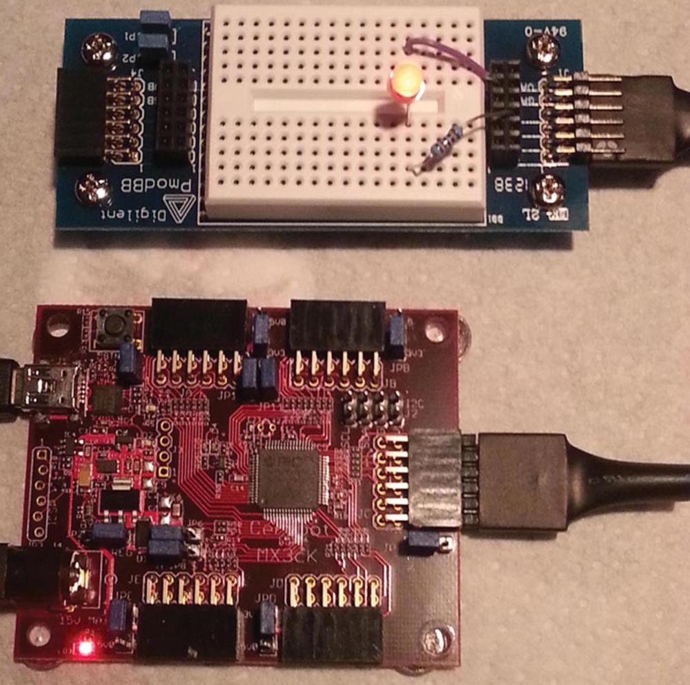
FIGURE 7.36 The PmodBB Module and chipKIT MX3
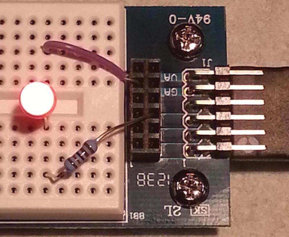
FIGURE 7.37 The PmodBB Module With LED and Resistor
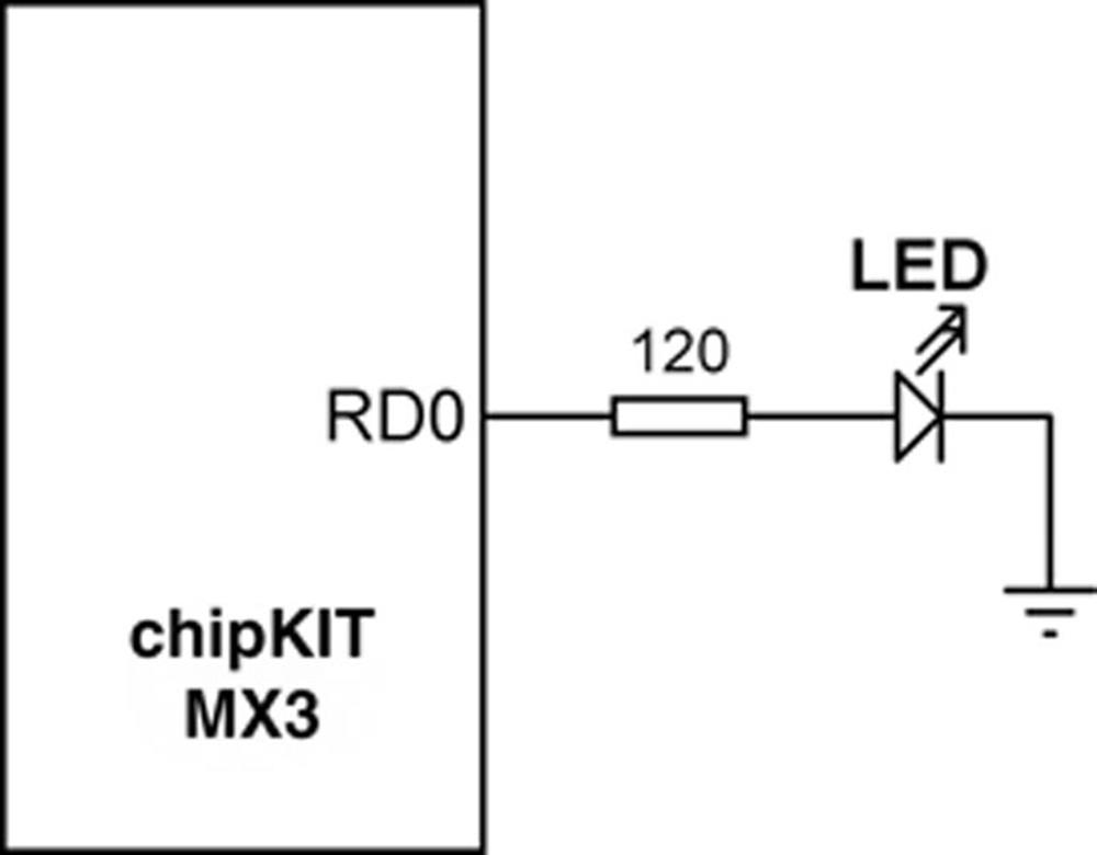
FIGURE 7.38 Circuit Diagram of the Project
7.9.4. Project PDL
The operation of the project is described in the PDL given in Figure 7.39. At the beginning of the program, logical port pin 22 is configured as output. Then, inside the main program loop, a PWM signal is sent to the port with varying duty cycle. As a result, the LED brightness increases gradually.

FIGURE 7.39 PDL of the Project
7.9.5. Project Program
The program is called FADE, and the program listing is shown in Figure 7.40. At the beginning of the program, logical port 22 (port pin RD0) is configured as output. Then, inside the main program loop, function analogWrite is used to send a PWM signal to the port with varying duty cycle. The duty cycle varies between 0 (LED OFF) and 255 (full brightness) in steps of five and with a delay of 100 ms between each output.
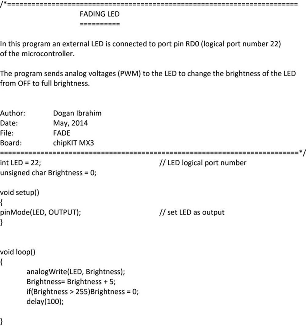
FIGURE 7.40 Program Listing of the Project
7.10. Project 7.10 – Seven-Segment LED
7.10.1. Project Description
In this project, a two-digit seven-segment LED is designed to display the number “27.” The project shows how a two-digit seven-segment LED can be interfaced and used with the chipKIT MX3 development board.
Seven-segment displays are basically LED-based displays, used frequently in electronic circuits to show numeric or alphanumeric values. As shown in Figure 7.41, a seven-segment display basically consists of seven LEDs connected such that numbers from 0 to 9 and some letters can be displayed when appropriate segments of the LEDs are turned ON. Segments are identified by letters from a to g, and Figure 7.42 shows the segment names of a typical seven-segment display.
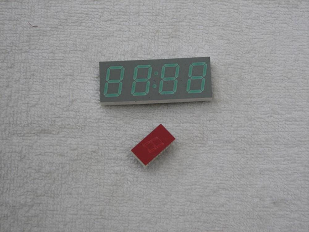
FIGURE 7.41 Four-Digit and One-Digit Seven-Segment Displays
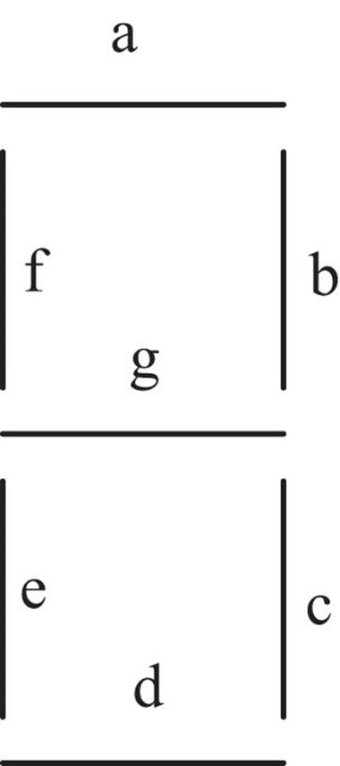
FIGURE 7.42 Segment Names of a Seven-Segment Display
Figure 7.43 shows how numbers from 0 to 9 can be obtained by turning ON different LED segments of the display.
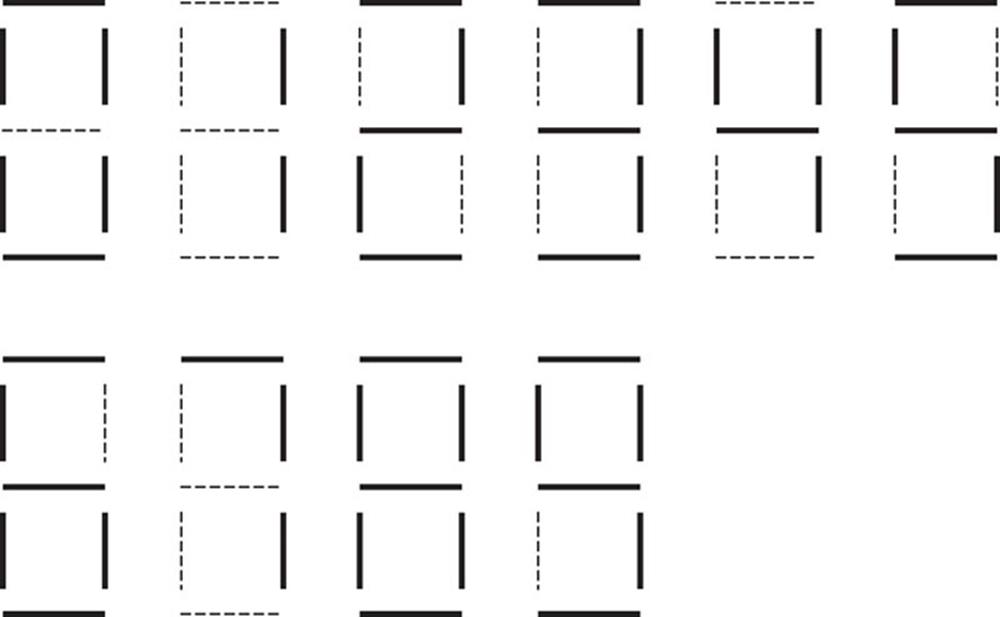
FIGURE 7.43 Displaying Numbers 0–9
Seven-segment displays are available in two different configurations: common cathode and common anode. As shown in Figure 7.44, in common cathode configuration, all the cathodes of all LED segments are connected together to ground. The segments are turned ON by applying a logic 1 to the required LED segment via current-limiting resistors. In common cathode configuration, the seven-segment LED is connected to the microcontroller in current-sourcing mode.
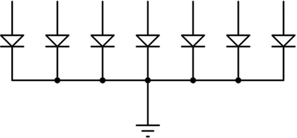
FIGURE 7.44 Common Cathode Seven-Segment Display
In a common anode configuration, the anode terminals of all the LEDs are connected together as shown in Figure 7.45. This common point is then normally connected to the supply voltage. A segment is turned ON by connecting its cathode terminal to logic 0 via a current-limiting resistor. In common anode configuration, the seven-segment LED is connected to the microcontroller in current-sinking mode.
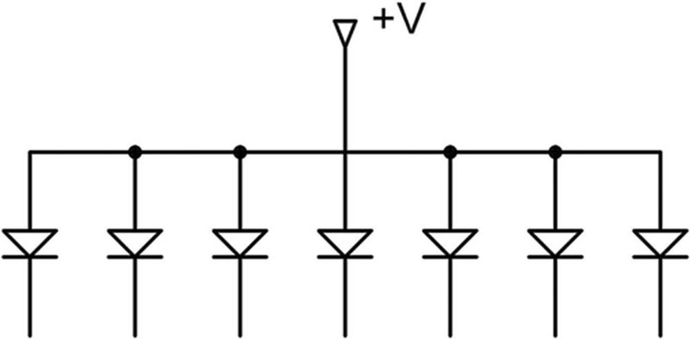
FIGURE 7.45 Common Anode Seven-Segment Display
In seven-segment display applications, a table is normally constructed that shows the relationship between the numbers to be displayed and the LED segments that should be turned ON to display the required number. In single-digit applications (to display 0–9), the common pin is connected to ground or to +V supply depending on whether the display is of type common cathode or common anode.
In multidigit seven-segment display applications (see Figure 7.46), digit pins are tied in parallel except the common pins. The common pin of each digit is turned ON alternately by the microcontroller. By displaying each digit for several milliseconds, the eye cannot differentiate that the digits are not ON all the time. This way we can multiplex any number of seven-segment displays together. For example, to display number 45, we have to send 4 to the first digit and enable its common pin. After a few milliseconds, number 5 is sent to the second digit and the common point of the second digit is enabled. When this process is repeated continuously, the user sees as if both displays are ON continuously.
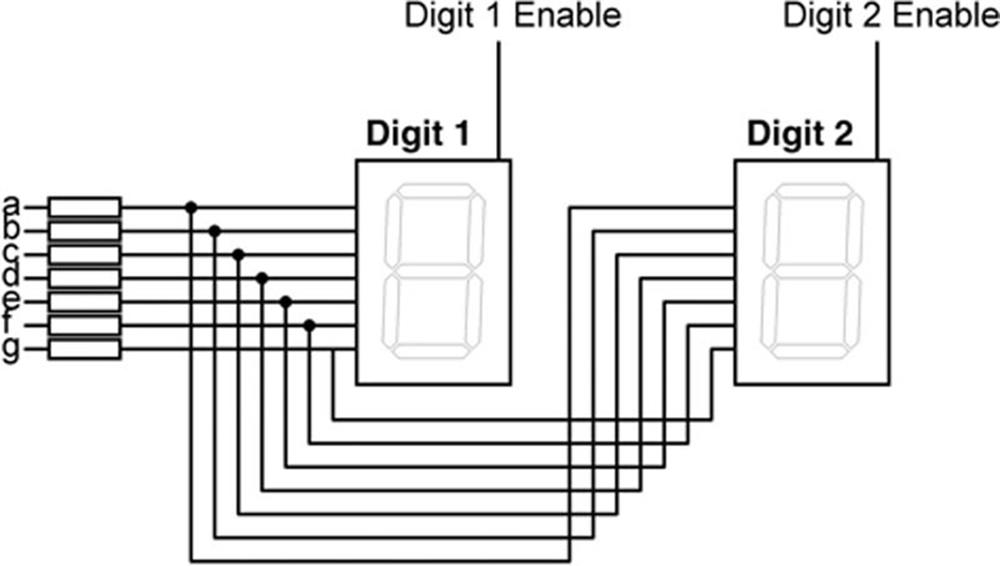
FIGURE 7.46 Multiplexed Two-Digit Seven-Segment Displays
Some manufacturers provide multiplexed multidigit displays in single packages. For example, we can purchase two-, four-, or eight-digit multiplexed displays in a single package. As an example, a two-digit display can be controlled from the microcontroller as follows:
• Send the segment bit pattern for digit 1 to segments a–g.
• Enable digit 1.
• Wait for a few milliseconds.
• Disable digit 1.
• Send the segment bit pattern for digit 2 to segments a–g.
• Enable digit 2.
• Wait for a few milliseconds.
• Disable digit 2.
• Repeat the above process continuously.
In this project, a two-digit, seven-segment Pmod-compatible display module called PmodSSD is used. The block diagram of the project is shown in Figure 7.47.
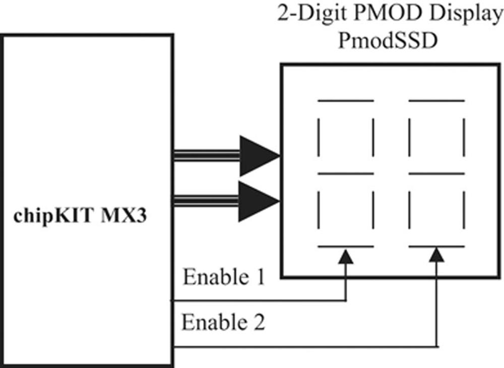
FIGURE 7.47 Block Diagram of the Project
7.10.2. Project Hardware
As shown in Figure 7.48, PmodSSD module is a high-brightness two-digit, common cathode seven-segment display with built-in current-limiting resistors. Figure 7.49 shows the connection diagram of the display.
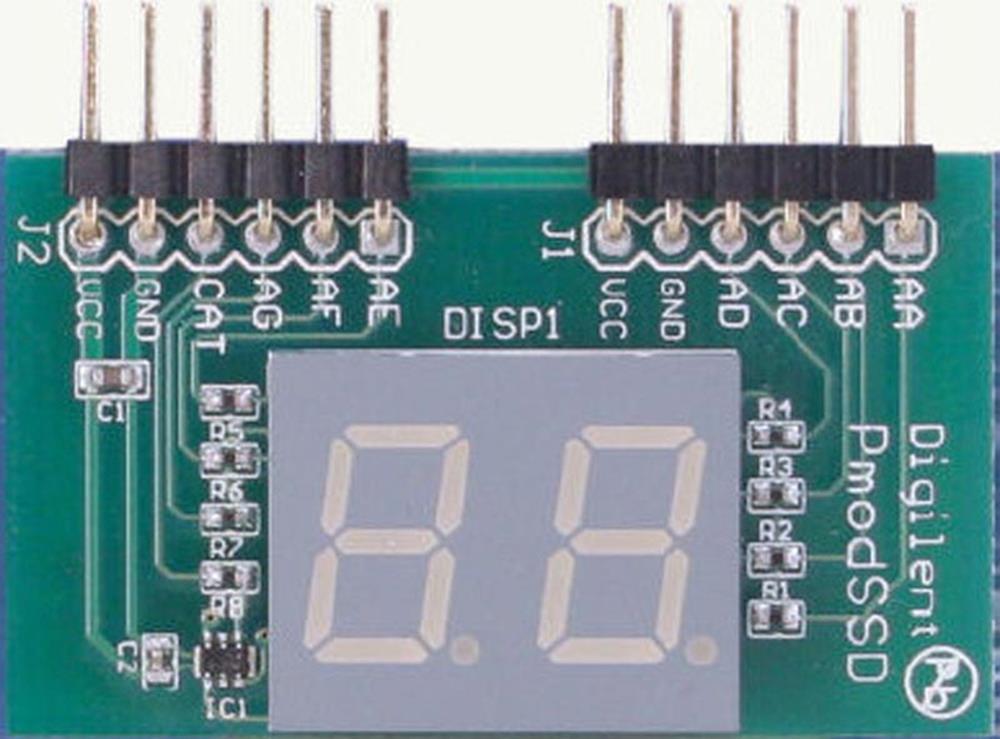
FIGURE 7.48 PmodSSD Two-Digit Seven-Segment Display Module
FIGURE 7.49 Connection Diagram of PmodSSD Module
The PmodSSD module has 2 × 6 pins, and in this project the module is connected to PMOD connectors JA and JB. Therefore, the relationship between the port numbers, port names, and PmodSSD segment are as in Table 7.1. Table 7.2 shows the logical port numbers of the JA and JB connectors. Notice that the digits are enabled from bit 3 of connector JB. The logical port numbers and the bits to be sent to these port pins are shown in Table 7.3 where the horizontal numbers from 0 to 9 are the numbers to be displayed on a digit and numbers on the left-hand side (0, 1, 2, 3, 8, 9, 10) are the logical port numbers. As an example, to display number 2 on the MSD position, we have to send the following bits to the logical ports:
|
Logical Port Number |
Data to Be Sent |
|
0 |
1 |
|
1 |
1 |
|
2 |
0 |
|
3 |
1 |
|
8 |
1 |
|
9 |
0 |
|
10 |
1 |
Table 7.1
Relationship between ports and PmodSSD segments.
|
Number |
x |
g |
f |
e |
d |
c |
b |
a |
JB |
JA |
|
0 |
c |
0 |
1 |
1 |
1 |
1 |
1 |
1 |
0x3 |
0xF |
|
1 |
c |
0 |
0 |
0 |
0 |
1 |
1 |
0 |
0x0 |
0x6 |
|
2 |
c |
1 |
0 |
1 |
1 |
0 |
1 |
1 |
0x5 |
0xB |
|
3 |
c |
1 |
0 |
0 |
1 |
1 |
1 |
1 |
0x4 |
0xF |
|
4 |
c |
1 |
1 |
0 |
0 |
1 |
1 |
0 |
0x6 |
0x6 |
|
5 |
c |
1 |
1 |
0 |
1 |
1 |
0 |
1 |
0x6 |
0xD |
|
6 |
c |
1 |
1 |
1 |
1 |
1 |
0 |
1 |
0x7 |
0xD |
|
7 |
c |
0 |
0 |
0 |
0 |
1 |
1 |
1 |
0x0 |
0x7 |
|
8 |
c |
1 |
1 |
1 |
1 |
1 |
1 |
1 |
0x7 |
0xF |
|
9 |
c |
1 |
1 |
0 |
1 |
1 |
1 |
1 |
0x6 |
0xF |
c is the control bit (0 = enable LSD; 1 = enable MSD).
Table 7.2
Logical pin numbers of connectors JA and JB.
|
JB-04 |
JB-03 |
JB-02 |
JB-01 |
JA-04 |
JA-03 |
JA-02 |
JA-01 |
|
11 |
10 |
9 |
8 |
3 |
2 |
1 |
0 |
|
RF06 |
RF02 |
RF03 |
RD09 |
RE03 |
RE02 |
RE01 |
RE00 |
Table 7.3
Logical port numbers and numbers to be displayed.
|
0 |
1 |
2 |
3 |
4 |
5 |
6 |
7 |
8 |
9 |
|
|
0 |
1 |
0 |
1 |
1 |
0 |
1 |
1 |
1 |
1 |
1 |
|
1 |
1 |
1 |
1 |
1 |
1 |
0 |
0 |
1 |
1 |
1 |
|
2 |
1 |
1 |
0 |
1 |
1 |
1 |
1 |
1 |
1 |
1 |
|
3 |
1 |
0 |
1 |
1 |
0 |
1 |
1 |
0 |
1 |
1 |
|
8 |
1 |
0 |
1 |
0 |
0 |
0 |
1 |
0 |
1 |
0 |
|
9 |
1 |
0 |
0 |
0 |
1 |
1 |
1 |
0 |
1 |
1 |
|
10 |
0 |
0 |
1 |
1 |
1 |
1 |
1 |
0 |
1 |
1 |
In addition, logical port number 11 must be set HIGH to enable the MSD.
The interface between the chipKIT MX3 and the display is shown in Figure 7.50. In this figure, the logical I/O port numbers are shown.
FIGURE 7.50 Display Interface
7.10.3. Project PDL
The operation of the project is described in the PDL given in Figure 7.51. At the beginning of the program, the logical ports used in the project are configured as outputs. Then, number 2 is sent to the display and the MSD is enabled. After a delay of 5 ms, number 7 is sent and the LSD is enabled. The display remains in this state for a further 5 ms. This process is repeated forever, thus displaying number 27.
FIGURE 7.51 PDL of the Project
7.10.4. Project Program
The program is called SSD1, and the program listing is shown in Figure 7.52. At the beginning of the program, logical port pins 0, 1, 2, 3, 8, 9, 10, and 11 are configured as outputs. An array called PmodSSD is created to store the logical pin numbers. Similarly, a two-dimensional array called segment is created to store the bit pattern for each number to be displayed. The program creates a loop for each digit, where inside these loops the logical ports where the display is connected to are selected and the correct column of array segment is accessed (indexed by the number to be displayed, 0–9) and the bits in this column are sent to the display so that the required number can be displayed.
FIGURE 7.52 Program Listing of the Project
Figure 7.53 shows the PmodSSD module connected to the chipKIT MX3 development board.
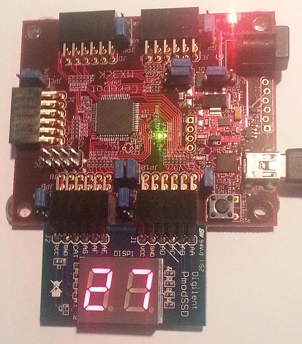
FIGURE 7.53 PmodSSD Module Displaying the Required Number
7.11. Project 7.11 – Seven-Segment Single-Digit LED Counter
7.11.1. Project Description
In this project, one digit of the two-digit PmodSSD module is used to count up from 0 to 9 with 1-s delay between each count.
7.11.2. Project Hardware
In this project, the PmodSSD is connected to connectors JA and JB as in Project 7.10 and only the MSD is used.
7.11.3. Project PDL
The operation of the project is described in the PDL given in Figure 7.54. At the beginning of the program, the logical ports used in the project are configured as outputs. Then, the value of a variable that is incremented every second is sent to the MSD of the display. Thus, the display counts as 0, 1, 2, 3, 4, 5, 6, 7, 8, 9, 0, 1, ….
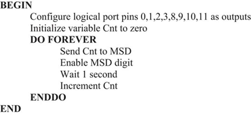
FIGURE 7.54 PDL of the Project
7.11.4. Project Program
The program is called SSD2, and the program listing is shown in Figure 7.55. At the beginning of the program, logical port pins 0, 1, 2, 3, 8, 9, 10, and 11 are configured as outputs. An array called PmodSSD is created to store the logical pin numbers. Similarly, an array called segment is created to store the bit pattern for the number to be displayed. Variable Cnt is used as the counter. The program creates a loop for the digit, where inside the loop the logical ports where the display is connected to are selected and the correct column of array segment is accessed (indexed by variable Cnt) and the bits in this column are sent to the display so that the value of Cnt can be displayed.
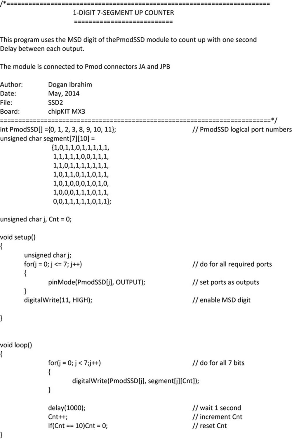
FIGURE 7.55 Program Listing of the Project
7.12. Project 7.12 – Using LCD Display
7.12.1. Project Description
In this project, the use of an LCD display is described. The project displays the text “chipKIT MX3” on the first row of an LCD.
In microcontroller systems, the output of a measured variable is usually displayed using LEDs, seven-segment displays, or LCD-type displays. LCDs have the advantages that they can be used to display alphanumeric or graphical data. Some LCDs have 40 or more character lengths with the capability to display several lines. Some other LCD displays can be used to display graphics images. Some modules offer colour displays while some others incorporate backlighting so that they can be viewed in dimly lit conditions.
There are basically two types of LCDs as far as the interface technique is concerned: parallel LCDs and serial LCDs. Parallel LCDs (e.g., Hitachi HD44780) are connected to a microcontroller using more than one data line and the data is transferred in parallel form. It is common to use either four or eight data lines. Using a four-wire connection saves I/O pins, but it is slower since the data is transferred in two stages. Serial LCDs are connected to the microcontroller using only one data line, and data is usually sent to the LCD using the standard RS-232 asynchronous data communication protocol. Serial LCDs are much easier to use, but they cost more than the parallel ones.
The programming of a parallel LCD is usually a complex task and requires a good understanding of the internal operation of the LCD controllers, including the timing diagrams. Fortunately, most high-level languages provide special library commands for displaying data on alphanumeric as well as on graphical LCDs. All the user has to do is connect the LCD to the microcontroller, define the LCD connection in the software, and then send special commands to display data on the LCD.
7.12.2. HD44780 LCD Module
HD44780 is one of the most popular alphanumeric LCD modules used in industry and also by hobbyists. This module is monochrome and comes in different sizes. Modules with 8, 16, 20, 24, 32, and 40 columns are available. Depending on the model chosen, the number of rows varies between 1, 2, and 4. The display provides a 14-pin (or 16-pin) connector to a microcontroller. Table 7.4 gives the pin configuration and pin functions of a 14-pin LCD module. Below is a summary of the pin functions.
Table 7.4
Pin configuration of HD44780 LCD module.
|
Pin No. |
Name |
Function |
|
1 |
VSS |
Ground |
|
2 |
VDD |
Positive supply |
|
3 |
VEE |
Contrast |
|
4 |
RS |
Register select |
|
5 |
R/W |
Read/write |
|
6 |
E |
Enable |
|
7 |
D0 |
Data bit 0 |
|
8 |
D1 |
Data bit 1 |
|
9 |
D2 |
Data bit 2 |
|
10 |
D3 |
Data bit 3 |
|
11 |
D4 |
Data bit 4 |
|
12 |
D5 |
Data bit 5 |
|
13 |
D6 |
Data bit 6 |
|
14 |
D7 |
Data bit 7 |
VSS is the 0 V supply or ground. The VDD pin should be connected to the positive supply. Although the manufacturers specify a 5 V D.C. supply, the modules will usually work with as low as 3 V or as high as 6 V.
Pin 3 is named VEE, and this is the contrast control pin. This pin is used to adjust the contrast of the display, and it should be connected to a variable voltage supply. A potentiometer is normally connected between the power supply lines with its wiper arm connected to this pin so that the contrast can be adjusted.
Pin 4 is the register select (RS), and when this pin is LOW, data transferred to the display is treated as commands. When RS is HIGH, character data can be transferred to and from the module.
Pin 5 is the read/write (R/W) line. This pin is pulled LOW in order to write commands or character data to the LCD module. When this pin is HIGH, character data or status information can be read from the module.
Pin 6 is the enable (E) pin that is used to initiate the transfer of commands or data between the module and the microcontroller. When writing to the display, data is transferred only on the HIGH-to-LOW transition of this line. When reading from the display, data becomes available after the LOW-to-HIGH transition of the enable pin, and this data remains valid as long as the enable pin is at logic HIGH.
Pins 7–14 are the eight data bus lines (D0–D7). Data can be transferred between the microcontroller and the LCD module either using a single 8-bit byte or as two 4-bit nibbles. In the latter case, only the upper four data lines (D4–D7) are used. 4-Bit mode has the advantage that four less I/O lines are required to communicate with the LCD.
7.12.3. Connecting the LCD to the Microcontroller
In this book, the Pmod LCD module called PmodCLP (Pmod Character Parallel LCD) is used in 8-bit mode. As shown in Figure 7.56, this module has two Pmod connectors: a dual connector called J1 and a single connector called J2 (see Figure 7.57). The module contains a 3.3–5 V converter for the LCD. The interface contains eight data signals and three control signals. The three control signals are the R/W, RS, and E.
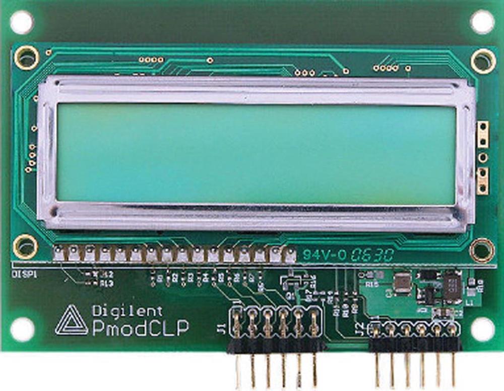
FIGURE 7.56 PmodCLP Module
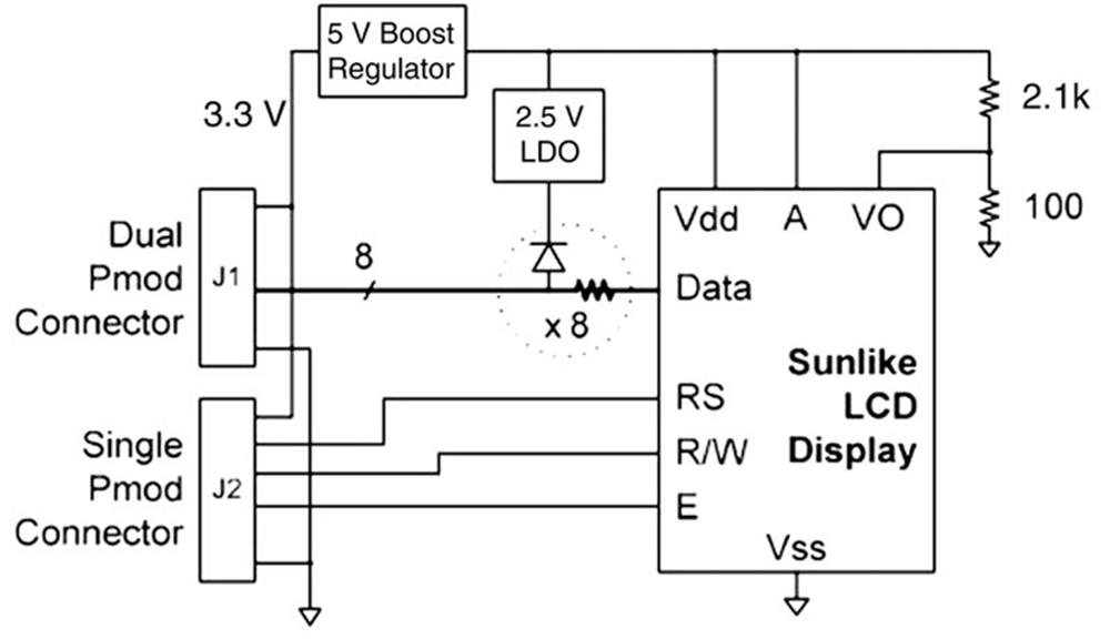
FIGURE 7.57 PmodCLP Connection Diagram
In this project, the PmodCLP module is connected to Pmod connectors JA and JB. The interface between the LCD module and the Pmod connectors is shown in Table 7.5. The brightness of the display is set by a resistive potential divider consisting of a 100 Ω and a 2.1k resistor.
Table 7.5
PmodCLP interface.
|
Connector Pin |
Logical I/O Port Number |
Port Name |
LCD Pin |
LCD Pin Name |
|
JA-01 |
0 |
RE0 |
D0 |
Data 0 |
|
JA-02 |
1 |
RE1 |
D1 |
Data 1 |
|
JA-03 |
2 |
RE2 |
D2 |
Data 2 |
|
JA-04 |
3 |
RE3 |
D3 |
Data 3 |
|
JA-07 |
4 |
RE4 |
D4 |
Data 4 |
|
JA-08 |
5 |
RE5 |
D5 |
Data 5 |
|
JA-09 |
6 |
RE6 |
D6 |
Data 6 |
|
JA-10 |
7 |
RE7 |
D7 |
Data 7 |
|
JB-07 |
12 |
RD6 |
RS |
Register select |
|
JB-08 |
13 |
RD5 |
R/W |
Read/write |
|
JB-09 |
14 |
RD4 |
E |
Enable |
7.12.4. Project Hardware
Figure 7.58 shows the connection between the PmodCLP module and the chipKIT MX3 development board. Here, the logical I/O port numbers are shown.
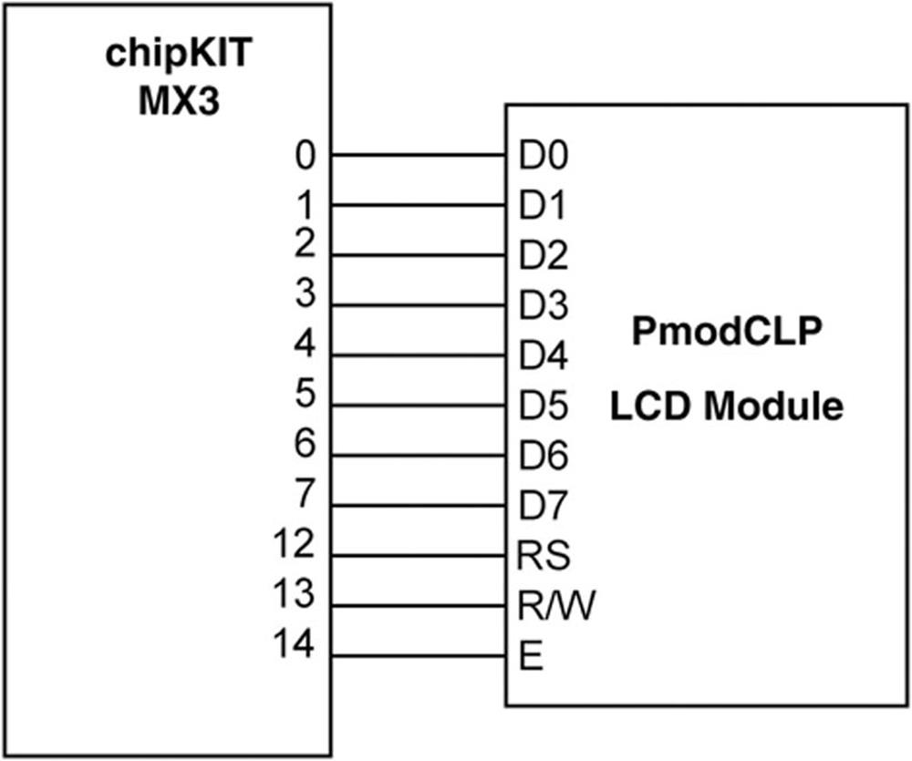
FIGURE 7.58 PmodCLP Interface to the Development Board
7.12.5. LCD Functions
There are many LCD functions that can be used to control the standard HD44780 or compatible LCD. The header file LiquidCrystal.h must be included at the beginning of the program by importing this library into the MPIDE IDE. Some commonly used functions are described in this section briefly (in these functions, variable name lcd is used).
LiquidCrystal lcd(rs, rw, e, d0, d1, d2, d3, d4, d5, d6, d7): This function creates a variable called lcd of type LiquidCrystal and is used to define the interface between the microcontroller logical I/O port numbers and the LCD.
lcd.begin(col, row): This function must be called before any other LCD function, and it initialises the LCD size by specifying its number of rows and columns.
lcd.clear(): This function clears the LCD screen and positions the cursor in the top left-hand corner.
lcd.home(): This function homes the cursor by positioning it in the top left-hand corner.
lcd.setCursor(col, row): This function positions the cursor at the specified column and row position.
lcd.write(byte): This function writes a character (or byte) at the current cursor position.
lcd.print(text): This function writes the text at the current cursor position.
lcd.print(data, BIN|DEC|OCT|HEX): This function writes the data in the specified number base. The data can be byte, integer, long, or string.
lcd.blink() and lcd.noBlink(): These functions start or stop the cursor from blinking.
lcd.cursor and lcd.noCursor(): These functions enable or disable the display of the cursor.
lcd.scrollDisplayLeft() and lcd.scrollDisplayRight(): These functions scroll the display one position to the left or right.
7.12.6. Project PDL
The operation of the project is described in the PDL given in Figure 7.59. At the beginning of the program, the interface between the LCD and the chipKIT MX3 board is specified.

FIGURE 7.59 PDL of the Project
A variable called lcd of type LiquidCrystal is declared. Inside the main program, the text chipKIT MX3 is displayed starting from the home position of the display.
7.12.7. Project Program
The program is called LCD1, and the program listing is shown in Figure 7.60. At the beginning of the program, function LiquidCrystal is called to define the interface between the LCD and the logical I/O ports. Then, the text chipKIT MX3 is displayed starting from the home position of the cursor.
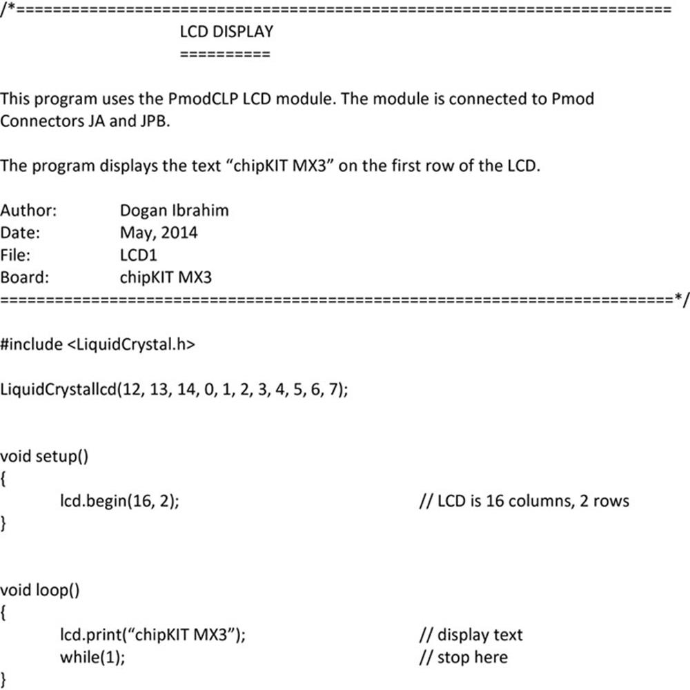
FIGURE 7.60 Program Listing of the Project
Figure 7.61 shows the PmodCLP module connected to the development board and displaying the required text.
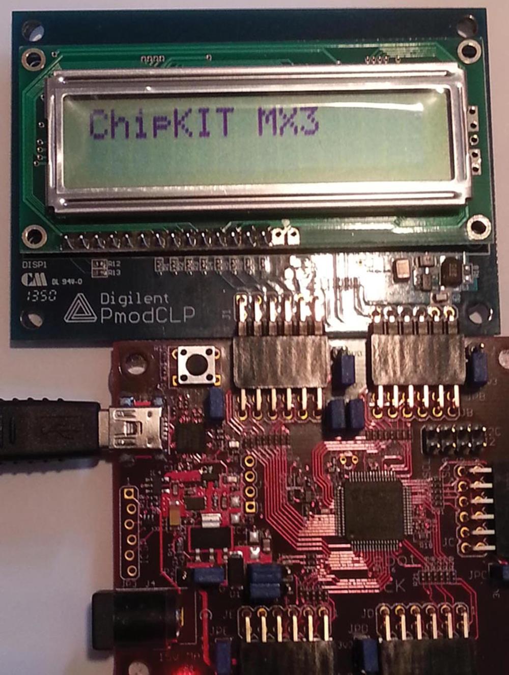
FIGURE 7.61 Displaying Text chipKIT MX3
7.13. Project 7.13 – Scrolling LCD Display
7.13.1. Project Description
In this project, it is shown how text displayed on the LCD can easily be scrolled left and right. The text chipKIT MX3 is initially displayed on the LCD. Then, this text is scrolled to the end of the screen towards the right and then towards the left of the display.
7.13.2. Project Hardware
In this project, the PmodCLP LCD module is used as in the previous project. The connection of the PmodCLP module to the chipKIT MX3 development board is as shown in Figure 7.58.
7.13.3. Project PDL
The operation of the project is described in the PDL shown in Figure 7.62. At the beginning of the program, the interface between the LCD and the chipKIT MX3 board is specified. A variable called lcd of type LiquidCrystal is declared. Inside the main program, the text chipKIT MX3 is initially displayed at the top row of the LCD. Then, the main program loop starts where the text is initially scrolled to the right to the end of the screen (16 positions). After this, the text is scrolled to the left (27 positions) and then to the right (27 positions) continuously. A small delay (200 ms) is used between each output.
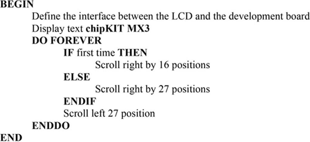
FIGURE 7.62 PDL of the Project
7.13.4. Project Program
The program is called LCD2, and the program listing is shown in Figure 7.63. At the beginning of the program, function LiquidCrystal is called to define the interface between the LCD and the logical I/O ports. Then, the text chipKIT MX3 is displayed starting from the home position of the cursor. Inside the main program, the text is scrolled to the right end of the LCD screen (by either 16 or 27 positions depending on whether this is the first iteration or not). Then, the text is scrolled to the left end of the screen by 27 positions. The program waits 200 ms before each output.
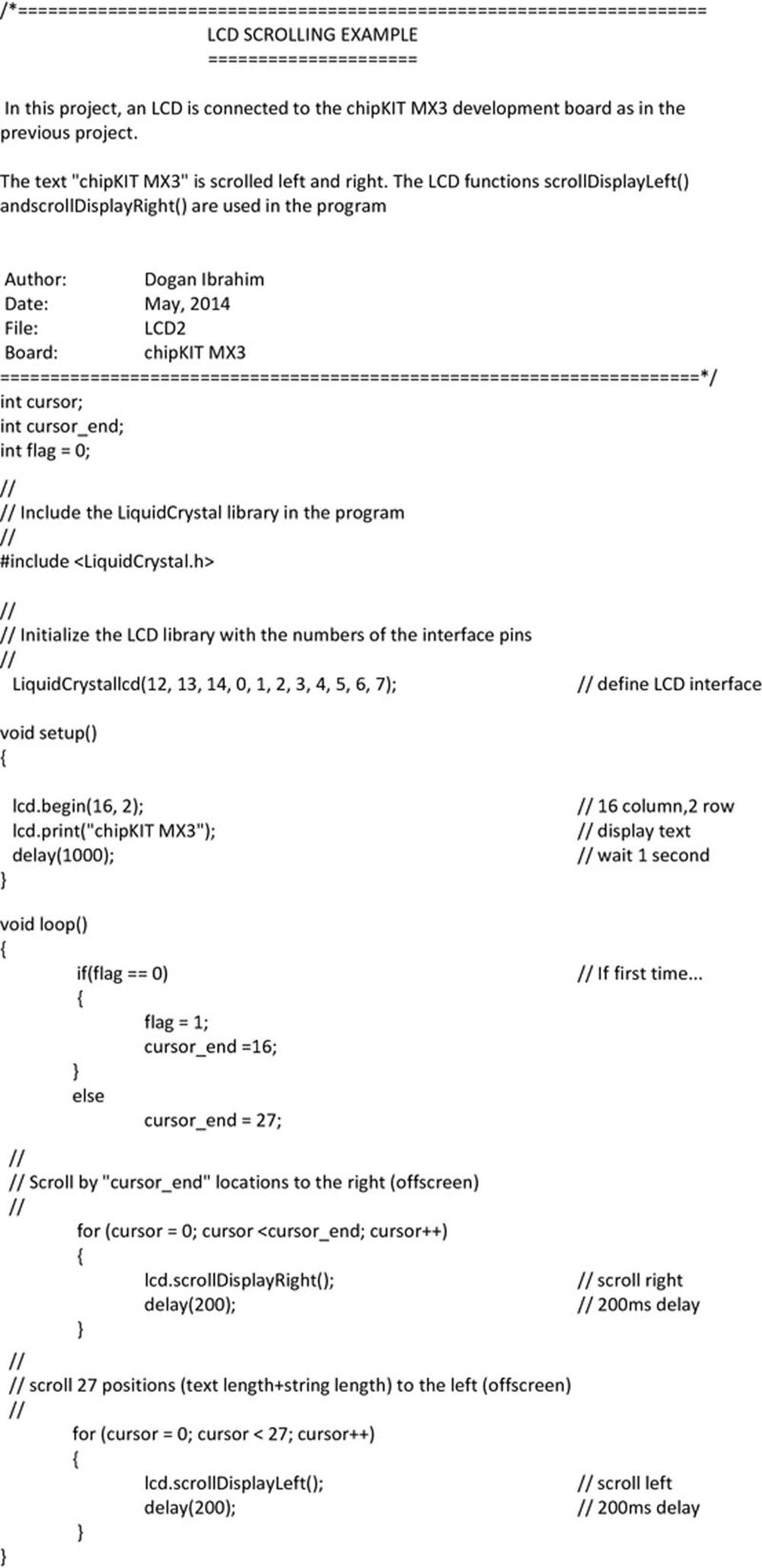
FIGURE 7.63 Program Listing of the Project
7.14. Project 7.14 – Seconds Counter With LCD Display
7.14.1. Project Description
In this project, the PmodCLP LCD module is connected to the chipKIT MX3 board as in the previous project. Here, the LCD counts up in seconds where the display is in the following format:
Count = nn
This project shows how the mixture of both text and numeric data can be displayed on the LCD.
7.14.2. Project Hardware
In this project, the PmodCLP LCD module is used as in the previous project. The connection of the PmodCLP module to the chipKIT MX3 development board is as shown in Figure 7.58.
7.14.3. Project PDL
The operation of the project is described in the PDL shown in Figure 7.64. At the beginning of the program, the interface between the LCD and the chipKIT MX3 board is specified. A variable called lcd of type LiquidCrystal is declared. An integer counter variablecnt is declared. Inside the main program, the value of this variable is displayed after the text Count =. The variable is incremented by 1, and the process is repeated after 1-s delay. Notice that in this program, the built-in function delay is used to create 1-s delay and as a result of this the timing is not accurate.
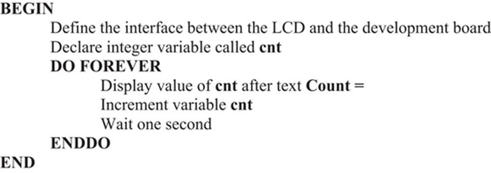
FIGURE 7.64 PDL of the Project
7.14.4. Project Program
The program is called LCD3, and the program listing is shown in Figure 7.65. At the beginning of the program, function LiquidCrystal is called to define the interface between the LCD module and the development board. Integer variable cnt is declared and set to 0. Inside the main program loop, the cursor is set to home position and the value of variable cnt is displayed after the text Count = . Variable cnt is then incremented by 1, and this process is repeated after 1-s delay.
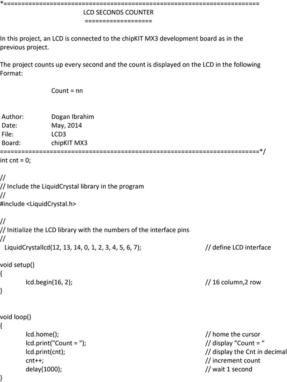
FIGURE 7.65 Program Listing of the Project
Figure 7.66 shows the LCD display as the program is running.
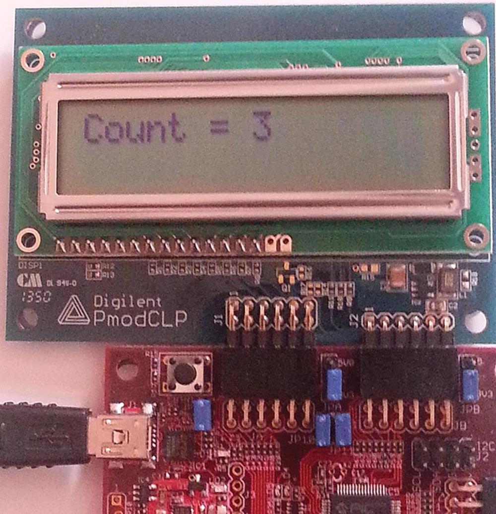
FIGURE 7.66 The LCD Display
7.15. Project 7.15 – Event Counter With LCD Display
7.15.1. Project Description
In this project, the PmodCLP LCD module is connected to the chipKIT MX3 board as in the previous project. Here, the LCD counts external events and displays the number of events on the LCD in the following format:
Event = nn
External events are said to occur when microcontroller pin RB08 (Pmod connector JPC pin JC-01, logical I/O port number 16) goes from logic 0 to logic 1. In this project, the PmodBTN button module is connected to Pmod connector JC and button BTN 0 is used to simulate an external event.
7.15.2. Project Hardware
In this project, the PmodCLP LCD module is connected to Pmod connectors JA and JB. The PmodBTN module is connected to the top row of Pmod connector JC. Thus, BTN0 is effectively connected to logical port number 16 (connector JC-01).
The connections of the PmodCLP and the PmodBTN modules to the chipKIT MX3 development board are as shown in Figure 7.67.
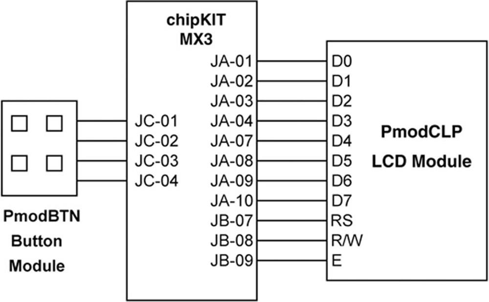
FIGURE 7.67 Connecting the PmodCLP and PmodBTN to the Development Board
7.15.3. Project PDL
The operation of the project is described in the PDL shown in Figure 7.68. At the beginning of the program, the interface between the LCD and the chipKIT MX3 board is specified. A variable called lcd of type LiquidCrystal is declared. An integer counter variablecnt is then declared and set to 0. Inside the main program, the push-button BTN0 is checked continuously, and when the button is pressed (BTN0 going from 0 to 1) and released (BTN going from 1 to 0), the value of cnt is incremented by 1 and its value is sent to the LCD. Thus, the LCD displays the number of external events occurring.
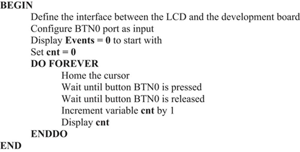
FIGURE 7.68 PDL of the Project
7.15.4. Project Program
The program is called LCD4, and the program listing is shown in Figure 7.69. At the beginning of the program, function LiquidCrystal is called to define the interface between the LCD module and the development board. Variable cnt is declared and is set to 0. Also, BTN0 is assigned to logical I/O port number 16. Inside the setup() function, the LCD is configured as 2 rows, 16 columns, BTN0 is configured as input port, the cursor is set to home position, and text Events = 0 is displayed to start with. Inside the main program loop, the state of BTN0 is checked continuously, and when the button is pressed (and then released), the value of cnt is incremented by 1 and its value is displayed on the LCD. Thus, the LCD displays the number of external events occurring.
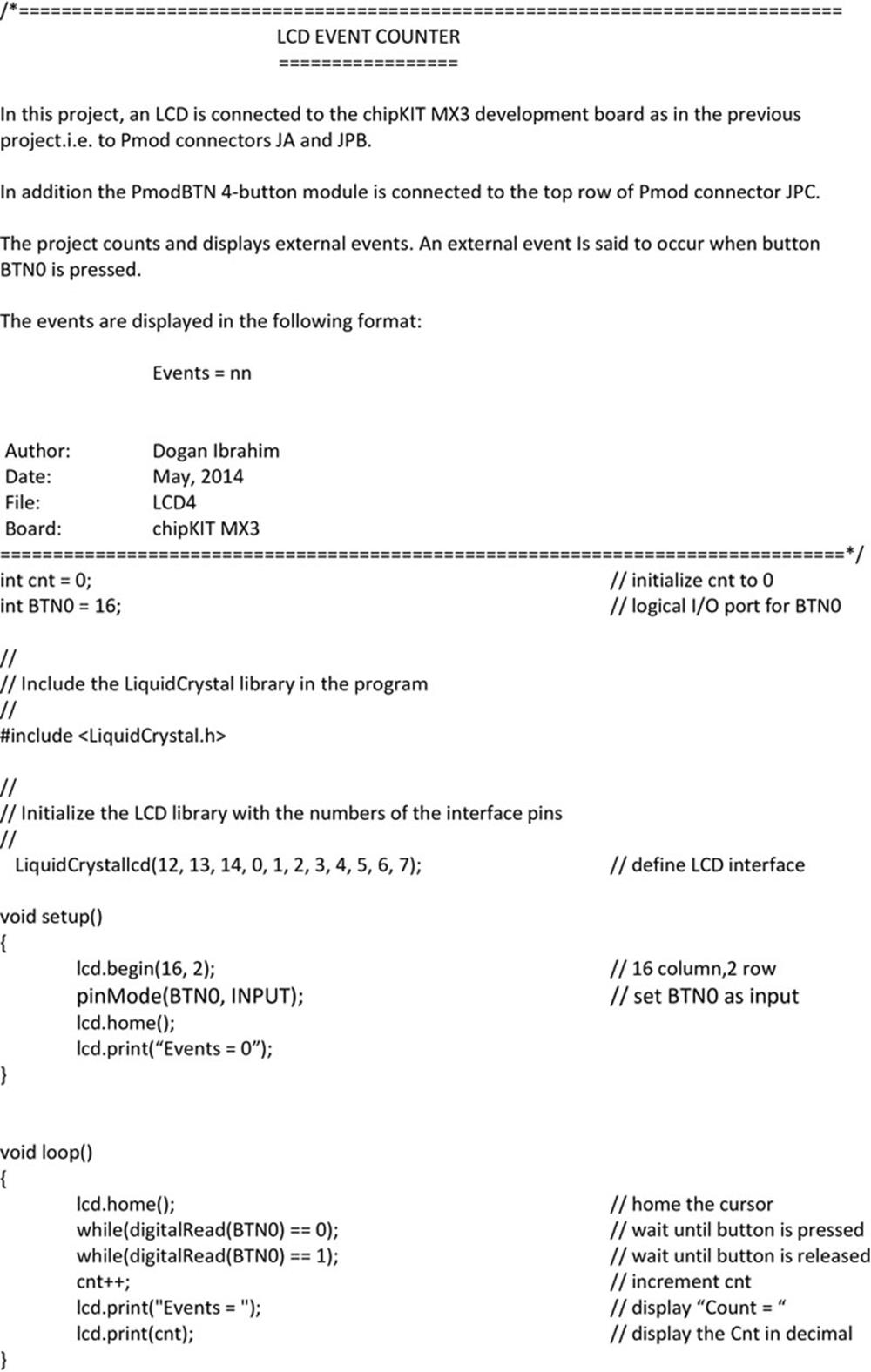
FIGURE 7.69 Program Listing of the Project
Figure 7.70 shows the project hardware setup.
FIGURE 7.70 Project Hardware Setup
7.16. Project 7.16 – External Interrupt–Driven Event Counter With LCD Display
7.16.1. Project Description
In this project, the PmodCLP LCD module is connected to Pmod connectors JA and JB as in the previous few projects. The PmodBTN module is used to generate an external interrupt when button BTN0 is pressed, and this simulates an external event. Inside the interrupt service routine, the value of a variable is incremented by 1 and then displayed on the LCD. Thus, the LCD displays the event count.
PIC32 microcontroller has five external interrupt sources INT0–INT4 (or EXT_INT0 to EXT_INT4). Using the MPIDE development environment, these interrupt sources are accessed using the attachInterrupt() and detachInterrupt() functions. The following Pmod connector positions are available for external interrupts:
INT0: JB-04, logical I/O port 11 (port pin RF6)
INT1: JE-07, logical I/O port 36 (port pin RD8)
INT2: JB-01, logical I/O port 8 (port pin RD9)
INT3: JD-03, logical I/O port 26 (port pin RD10)
INT4: JD-09, logical I/O port 39 (port pin RD11)
In this project, a PmodBTN four-button Pmod module is connected to the bottom row of Pmod connector JE. Thus, BTN0 corresponds to logical port number 36, that is, interrupt number 1 (INT1).
7.16.2. Project Hardware
The PmodCLP LCD module is connected to Pmod connectors JA and JB. The PmodBTN module is connected to the bottom row of Pmod connector JPE. Thus, BTN0 is effectively connected to logical port number 36 (connector JE-07).
The connections of the PmodCLP and the PmodBTN modules to the chipKIT MX3 development board are as shown in Figure 7.71.
FIGURE 7.71 Connecting the PmodCLP and PmodBTN to the Development Board
7.16.3. Project PDL
The operation of the project is described in the PDL shown in Figure 7.72. At the beginning of the program, the interface between the LCD and the chipKIT MX3 board is specified. A variable called lcd of type LiquidCrystal is declared. The interrupt service routine is then configured. A variable is incremented inside the interrupt service routine, and its value is sent to the display to show the event count.
FIGURE 7.72 PDL of the Project
7.16.4. Project Program
The program is called INT, and the program listing is shown in Figure 7.73. At the beginning of the program, function LiquidCrystal is called to define the interface between the LCD module and the development board. Variable cnt is declared and is set to 0. Inside the setup() function, the LCD is configured as 2 rows, 16 columns, the cursor is set to home position, and text Events = 0 is displayed to start with. In addition, function attachInterrupt is used to configure external interrupt INT1 such that the program jumps to routine ISR when the state of the external interrupt pin INT1 (interrupt number 1) changes from 0 to 1, that is, when the button is pressed.
FIGURE 7.73 Program Listing of the Project
Figure 7.74 shows the project hardware setup.
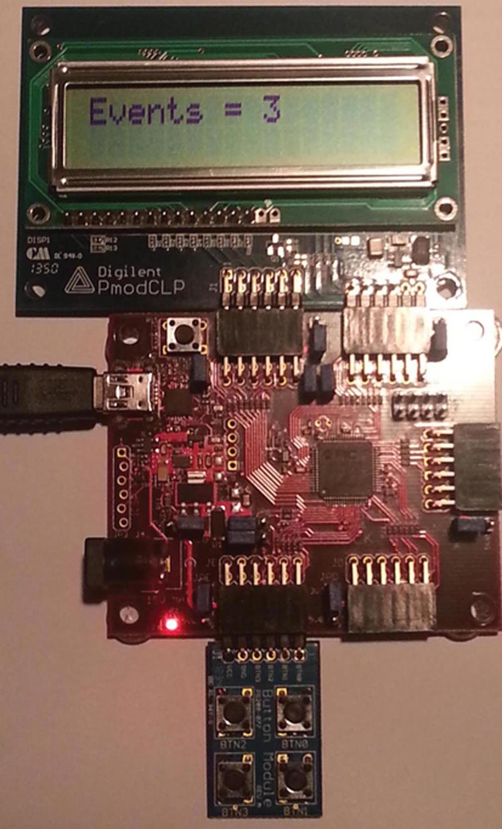
FIGURE 7.74 Project Hardware Setup
7.17. Project 7.17 – Voltmeter
7.17.1. Project Description
In this project, the analogue-to-digital converter (ADC) of the PIC32MX320 microcontroller is used to design a voltmeter. The project measures the external analogue voltage in the range 0 to +3.3 V and displays it on the LCD.
The PIC32MX320 microcontroller has 10-bit multiplexed ADC with 16 channels. The chipKIT MX3 development board provides access to 11 of these ADCs through the Pmod connectors. Because the ADC is 10-bit wide, the converted voltage has digital value in the range 0–1023.
The analogue inputs are accessed using the built-in function analogRead(). The analogue input pin number is specified using the symbols A0–A10 (the digital pin numbers 0–10 can also be used if desired).
The Pmod connector references, logical I/O pin numbers, and microcontroller pin names of the analogue channels are given as follows:
|
Analogue Channel |
Pmod Connector |
Digital Pin Number |
Microcontroller Pin |
|
A0 |
JC-01 |
16 |
RB8 |
|
A1 |
JC-04 |
19 |
RB14 |
|
A2 |
JC-07 |
20 |
RB0 |
|
A3 |
JC-08 |
21 |
RB1 |
|
A4 |
JD-01 |
24 |
RB2 |
|
A5 |
JD-04 |
27 |
RB9 |
|
A6 |
JD-07 |
28 |
RB12 |
|
A7 |
JD-10 |
31 |
RB13 |
|
A8 |
JE-08 |
37 |
RB5 |
|
A9 |
JE-09 |
38 |
RB4 |
|
A10 |
JE-10 |
39 |
RB3 |
In this project, analogue channel A0 is used. The external analogue voltage is applied directly to this pin.
The lower reference voltage for the ADC is Vref−, while the upper reference voltage is Vref+. The reference voltage can be either external or internal. When internal reference is used, Vref− is connected to Vss and Vref+ is connected to VDD. Thus, the reference voltage is +3.3 V and an input voltage of +3.3 V will convert to digital value 1023. When external reference is used, an external voltage source can be connected to the Vref+ input. In this case, Vref− is shared with AN1 (RB1), and Vref+ is shared with AN0 (RB0).
In this project, the internal voltage reference is used. Built-in function analogReference() is used to select the ADC reference voltage. The following reference voltage values can be selected:
• DEFAULT (Vref− = 0 and Vref+ = +3.3 V)
• INTERNAL (same as DEFAULT)
• EXTERNAL (Vref− = 0 and Vref+ = voltage at pin A2)
• EXTMINUS (Vref− = voltage at pin A3 and Vref+ = +3.3 V)
• EXTPLUSMINUS (Vref− = voltage at pin A3 and Vref+ = voltage at pin A2)
Figure 7.75 shows the block diagram of the project.
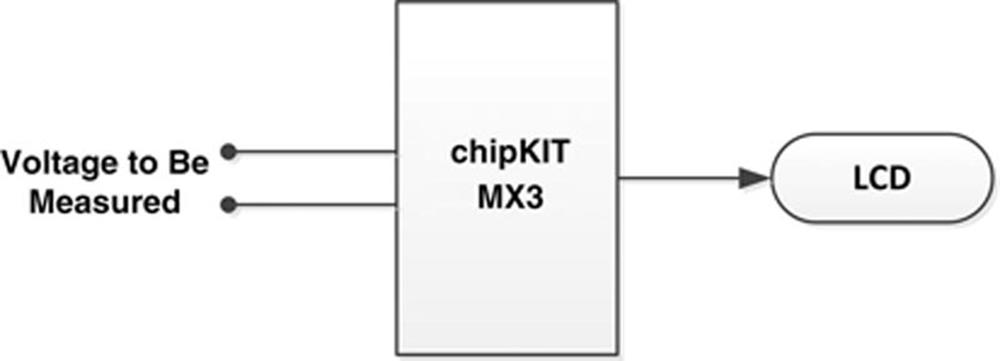
FIGURE 7.75 Block Diagram of the Project
7.17.2. Project Hardware
The voltage to be measured is applied to analogue input A0 (Pmod connector JC-01, logical I/O number 16, pin RB8). As shown in Figure 7.76, the PmodCLP LCD module is connected to Pmod connectors JA and JB as in the previous projects. External analogue voltages up to +3.3 V can be measured and displayed on the LCD. The breadboard Pmod module PmodBB is used to connect the voltage to be measured to Pmod connector JC-01. Pins JC-01 and JC-05 (ground) of connector JC are used to measure the external voltage. Figure 7.77 shows the hardware setup.
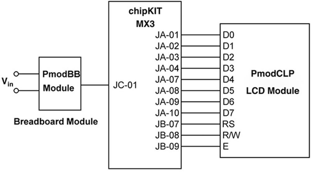
FIGURE 7.76 The Project Hardware
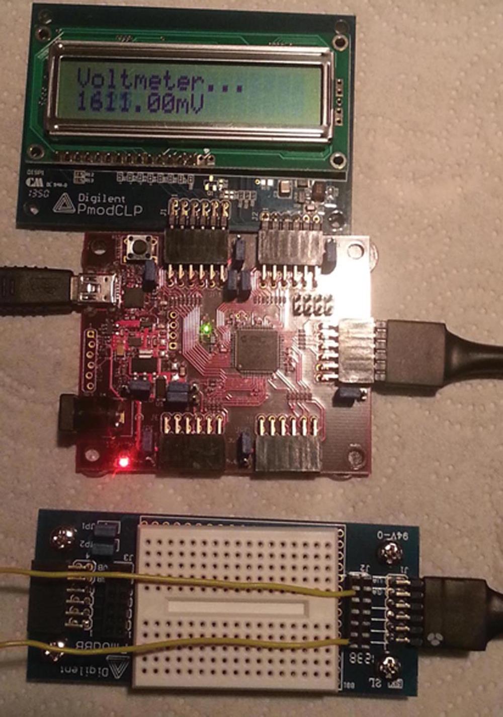
FIGURE 7.77 The Hardware Setup
7.17.3. Project PDL
The operation of the project is described in the PDL shown in Figure 7.78. At the beginning of the program, the interface between the LCD and the chipKIT MX3 board is specified. A variable called lcd of type LiquidCrystal is declared. The conversion factor is then defined that converts the read analogue input voltage into millivolts. A heading is displayed, and the ADC reference voltage is set to INTERNAL. The program then reads the analogue voltage and displays on the LCD every second.
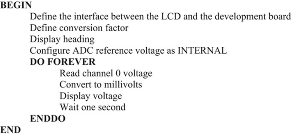
FIGURE 7.78 PDL of the Project
7.17.4. Project Program
The program is called VOLTMETER, and the program listing is shown in Figure 7.79. At the beginning of the program, function LiquidCrystal is called to define the interface between the LCD module and the development board. The conversion factor conv, when multiplied by the digital value, converts it into voltage in millivolts. The heading Voltmeter… is displayed on the top row of the LCD, and the ADC reference voltage is set to INTERNAL (+3.3 V). Inside the main program loop, the analogue voltage is read from channel 0 using function analogRead(Channel), where Channel is set to 0. The voltage in millivolts is then found by multiplying with conv and is displayed on the second row of the LCD. This process is repeated forever after 1-s delay.
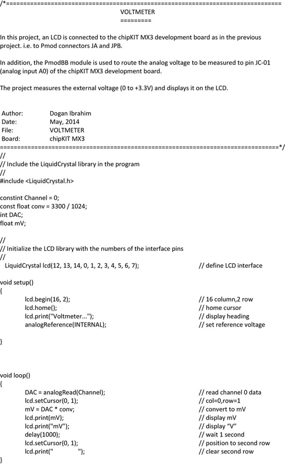
FIGURE 7.79 Program Listing of the Project
The design given in this circuit can be modified to measure higher input voltages by using potential divider resistors at the input circuit. For example, by attenuating the input voltage by about a factor of 10, input voltages up to 33 V can be measured. It is also recommended to use diodes at the input circuit to protect against excessive voltages and against reversed input polarity.
In Figure 7.80, the voltage at the ADC input is:

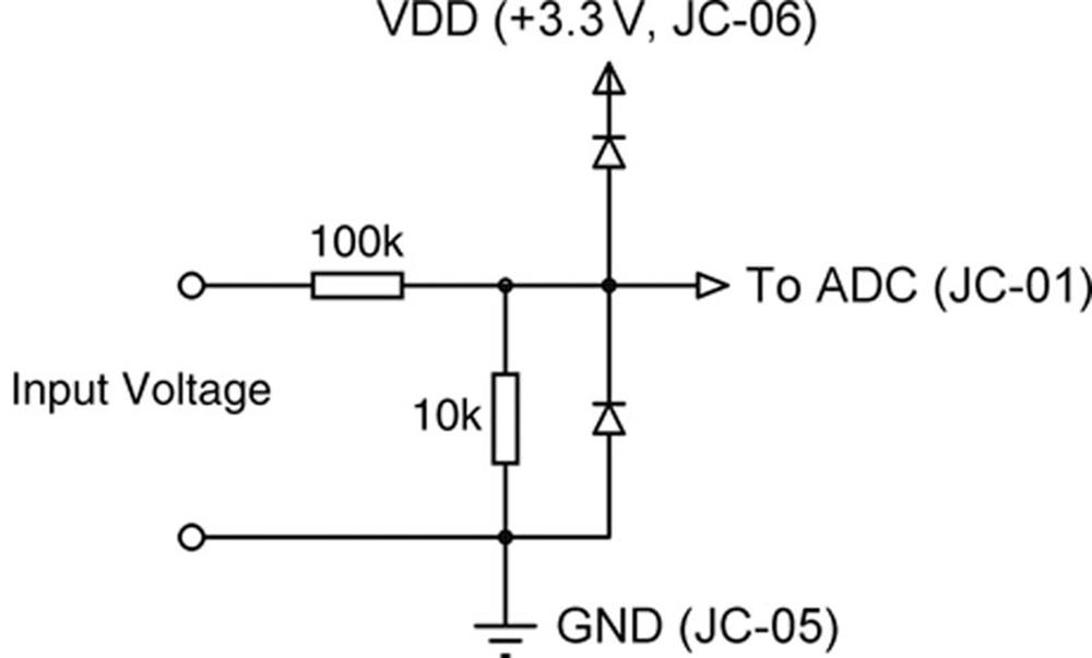
FIGURE 7.80 Increasing the Input Range
Thus, the maximum input voltage that can be measured is 3.3 V/0.0909 ≍ 36 V.
7.18. Project 7.18 – Temperature Measurement
7.18.1. Project Description
In this project, the ADC of the PIC32MX320 microcontroller is used to design a digital thermometer. The project measures the ambient temperature using a LM35DZ-type temperature sensor chip and then displays the temperature on the LCD in the following format:
Thermometer…
nn.nnC
In this project, analogue channel A0 is used as in the previous project. The output pin of the temperature sensor chip is directly connected to this channel. In this project, the internal voltage reference is used. Built-in function analogReference() is used to select the ADC reference voltage as INTERNAL (i.e., +3.3 V).
LM35DZ is a three-pin temperature sensor chip (see Figure 7.81 for pin configuration), having the following features:
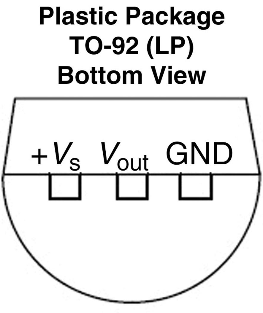
FIGURE 7.81 LM35DZ Temperature Sensor Pin Configuration
• Operation in the range of 4–39 V
• Measurement in the range of −55°C to +150°C
• Linear output voltage at 10 mV/°C
• Less than 60 μA current consumption
• Self-heating less than 0.1°C
• Plastic TO-92 transistor packaging
Figure 7.82 shows the block diagram of the project.
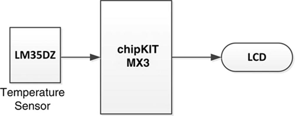
FIGURE 7.82 Block Diagram of the Project
7.18.2. Project Hardware
The LM35DZ temperature sensor chip is connected to analogue input A0 (Pmod connector JC-01, logical I/O number 16, pin RB8). As shown in Figure 7.83, the PmodCLP LCD module is connected to Pmod connectors JA and JB as in the previous projects. The breadboard Pmod module PmodBB is used to connect the LM35DZ chip to Pmod connector JC-01. Pmod JPC connector power supply selection jumper is set to +5 V since the LM35DZ requires at least 4 V for its operation.
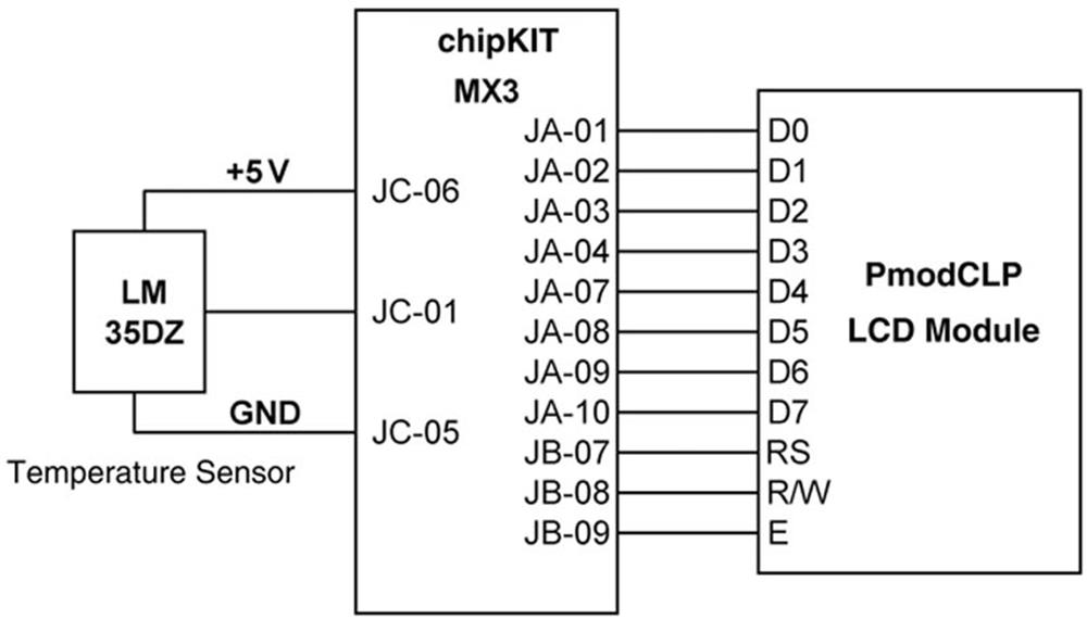
FIGURE 7.83 The Project Hardware
Figure 7.84 shows the hardware setup.
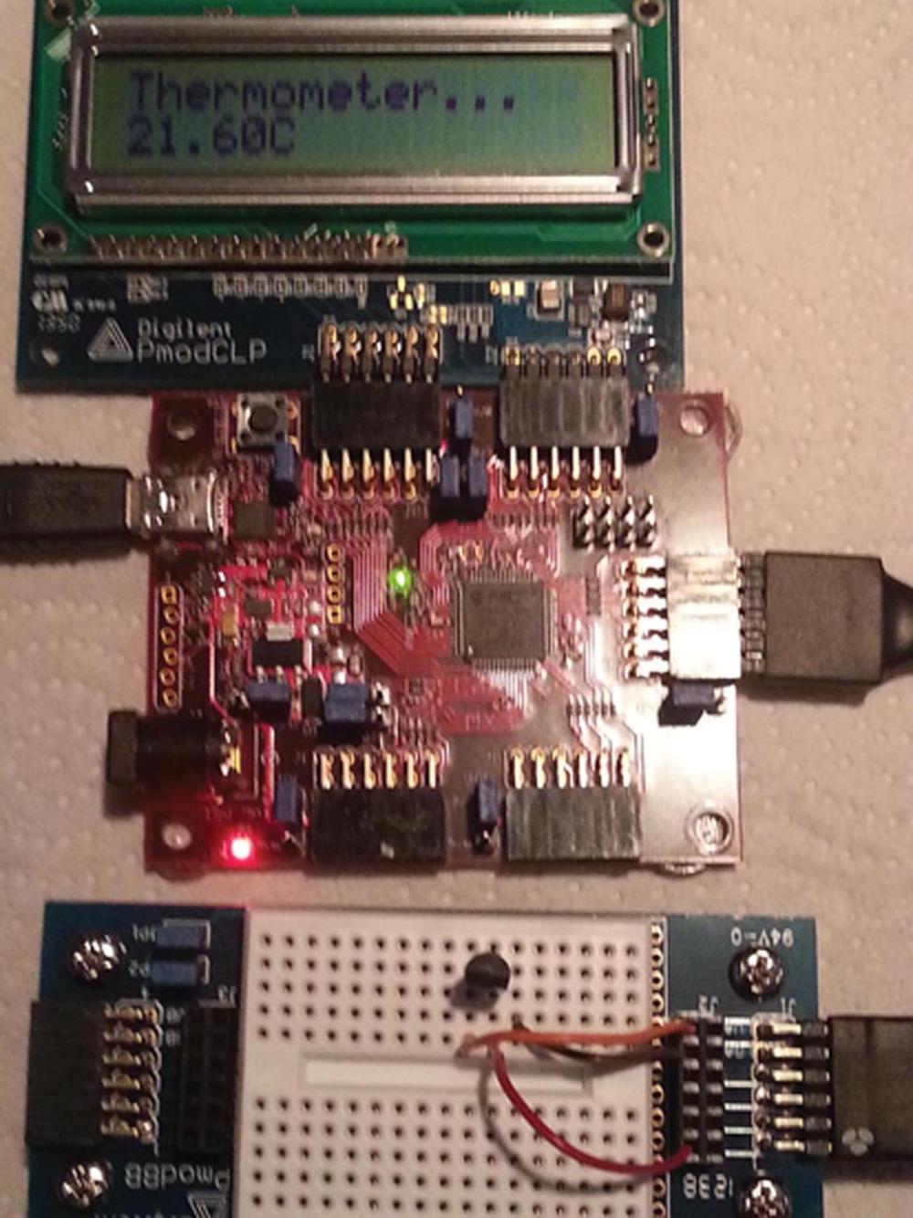
FIGURE 7.84 The Hardware Setup
7.18.3. Project PDL
The operation of the project is described in the PDL shown in Figure 7.85. At the beginning of the program, the interface between the LCD and the chipKIT MX3 board is specified. A variable called lcd of type LiquidCrystal is declared. The conversion factor is then defined that converts the read analogue input voltage into millivolts. A heading is displayed, and the ADC reference voltage is set to INTERNAL. The program then reads the analogue voltage, converts into millivolts, and divides by 10 to find and display the ambient temperature on the LCD every second.
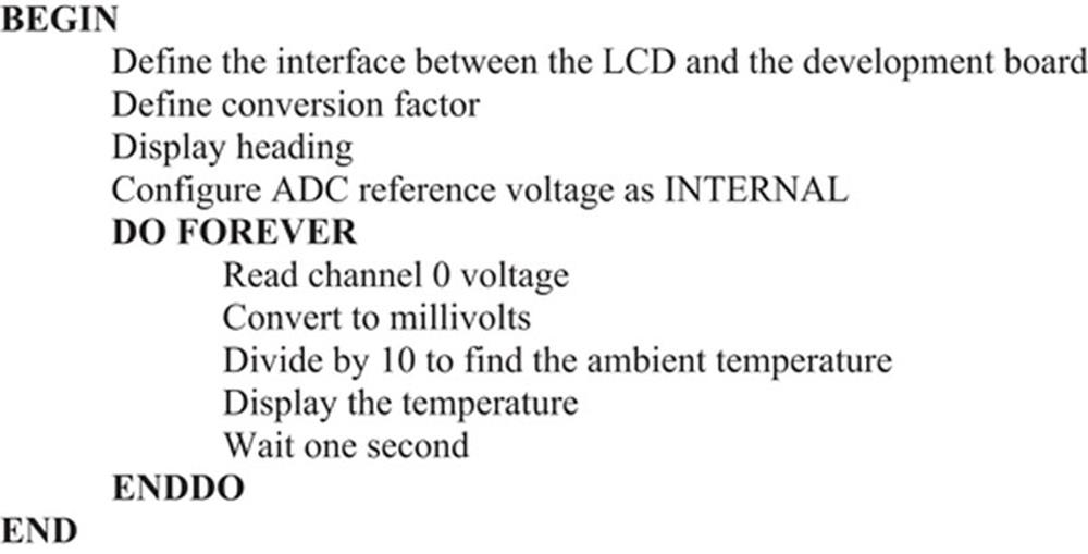
FIGURE 7.85 PDL of the Project
7.18.4. Project Program
The program is called THERMO1, and the program listing is shown in Figure 7.86. At the beginning of the program, function LiquidCrystal is called to define the interface between the LCD module and the development board. The conversion factor conv, when multiplied by the digital value, converts it into voltage in millivolts. The heading Thermometer… is displayed on the top row of the LCD, and the ADC reference voltage is set to INTERNAL (+3.3 V). Inside the main program loop, the analogue voltage is read from channel 0 using function analogRead(Channel), where Channel is set to 0. The voltage in millivolts is then found by multiplying with conv and then dividing by 10 to find the temperature in degrees centigrade. The temperature is displayed on the LCD every second.
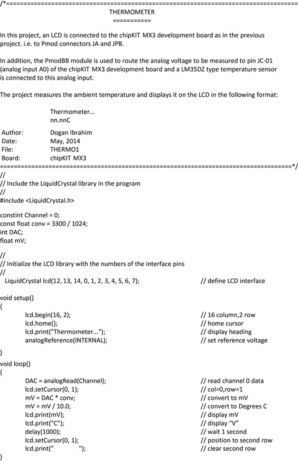
FIGURE 7.86 Program Listing of the Project
7.19. Project 7.19 – Temperature Measurement With Serial Monitor Display
7.19.1. Project Description
This project is very similar to the previous project where the ambient temperature is measured and displayed every second. In this project, the temperature is displayed on the MPIDE Serial Monitor.
In this project, the LM35DZ temperature sensor chip is used as in the previous project and is connected to analogue channel A0.
Figure 7.87 shows the block diagram of the project.
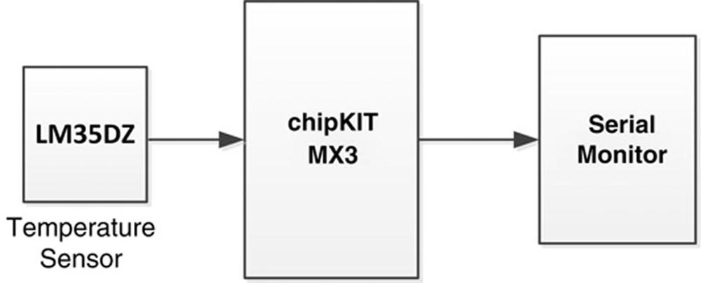
FIGURE 7.87 Block Diagram of the Project
7.19.2. Project Hardware
As shown in Figure 7.88, the LM35DZ temperature sensor chip is connected to analogue input A0 (Pmod connector JC-01, logical I/O number 16, pin RB8). The breadboard Pmod module PmodBB is used to connect the LM35DZ chip to Pmod connector JC-01. Pmod JPC connector power supply selection jumper is set to +5 V since the LM35DZ requires at least 4 V for its operation.
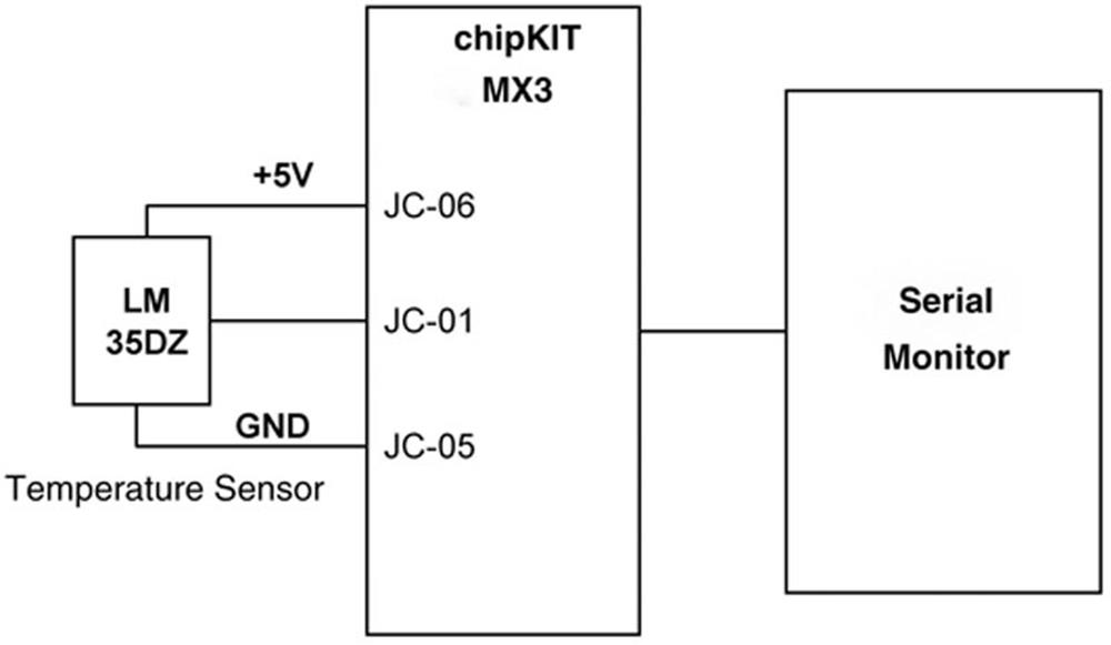
FIGURE 7.88 The Project Hardware
7.19.3. Project PDL
The operation of the project is described in the PDL shown in Figure 7.89. At the beginning of the program, the Serial Monitor interface is initialised to 9600 Baud. A heading is displayed, and the ADC reference voltage is set to INTERNAL. The program then reads the analogue voltage, converts into millivolts, and divides by 10 to find and display the ambient temperature on the Serial Monitor every second.
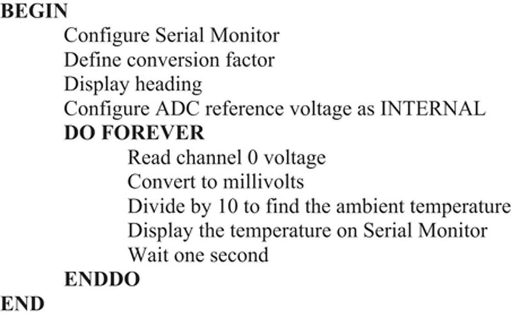
FIGURE 7.89 PDL of the Project
7.19.4. Project Program
The program is called THERMO2, and the program listing is shown in Figure 7.90. At the beginning of the program, the conversion factor conv, when multiplied by the digital value, converts it into voltage in millivolts. Serial Monitor is configured to operate at 9600 Baud using function Serial.begin(9600). The heading Thermometer… is displayed on the top row of the Serial Monitor using function Serial.print(“Thermometer…\n”), and the ADC reference voltage is set to INTERNAL (+3.3 V). Inside the main program loop, the analogue voltage is read from channel 0 using function analogRead(Channel), where Channel is set to 0. The voltage in millivolts is then found by multiplying with conv and then dividing by 10 to find the temperature in degrees centigrade. The temperature is displayed on the Serial Monitor every second as shown in Figure 7.91. Notice that a newline character (\n) is inserted at the end of the print command (the command Serial.println() could also be used to insert a newline after the display).
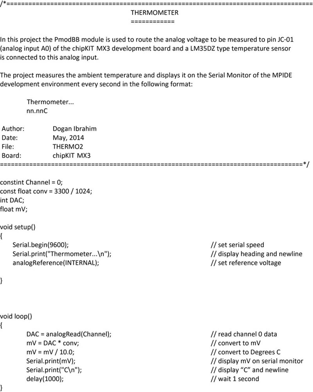
FIGURE 7.90 Program Listing of the Project
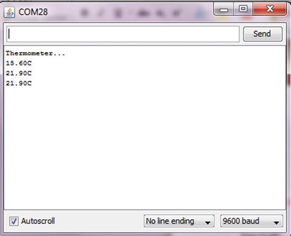
FIGURE 7.91 Displaying the Temperature on Serial Monitor
The Serial Monitor is accessed by clicking the menu options Tools → Serial Monitor on the MPIDE development environment.
7.20. Project 7.20 – NPN Transistor Tester
7.20.1. Project Description
This is an NPN transistor tester project. The project displays the various parameters of an NPN transistor on the Serial Monitor of the MPIDE development environment. The project demonstrates how two analogue ports of the microcontroller can easily be used.
The block diagram of the project is shown in Figure 7.92.
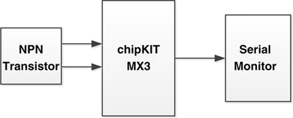
FIGURE 7.92 Block Diagram of the Project
7.20.2. Project Hardware
The transistor whose parameters are to be measured is connected to analogue ports A0 and A1 of the microcontroller as shown in the circuit diagram of Figure 7.93. The transistor is connected to the +3.3 V supply voltage (VCC) through a 1k resistor. The base of the transistor is connected to the collector through a 100k resistor.
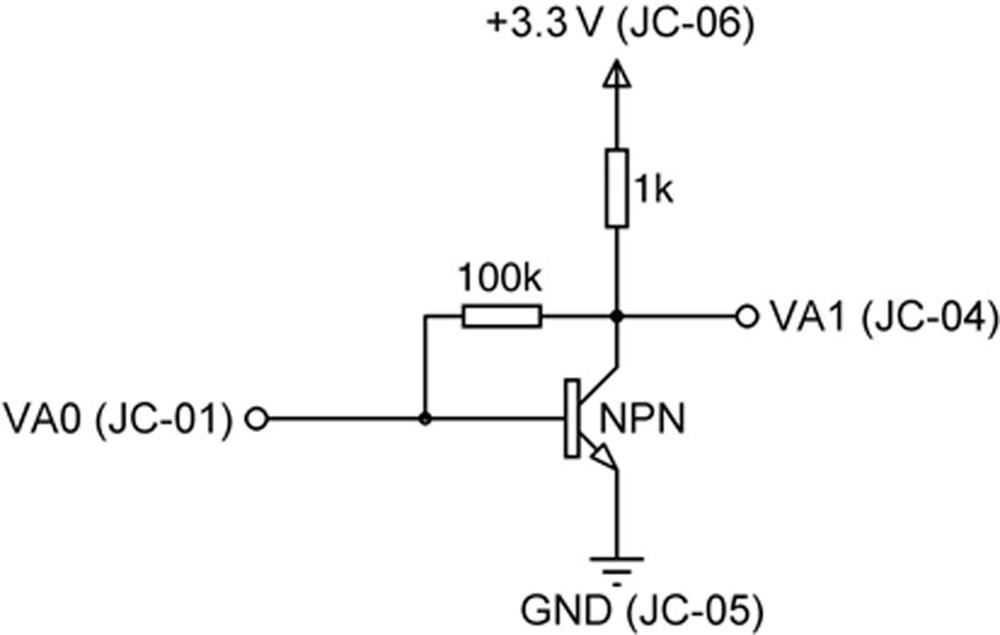
FIGURE 7.93 Project Circuit Diagram
In reference to Figure 7.93 and assuming a silicon-type transistor, we can write the following equations about the various parameters of an NPN transistor:
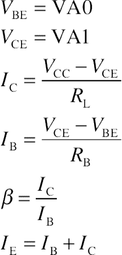
In this project, RL and RB are chosen as 1k and 100k, respectively. The ADC reference voltage is chosen as +3.3 V (INTERNAL). All the currents are expressed in milliamperes, and all the voltages are expressed in volts.
As shown in Figure 7.94, the base of the transistor is connected to analogue input A0 (Pmod connector JC-01, logical I/O number 16, pin RB8) and the collector is connected to A1 (Pmod connector JC-04, logical I/O number 19, pin RB14). The breadboard Pmod module PmodBB is used to connect the transistor to be tested to Pmod connector JC. The hardware setup is shown in Figure 7.95.
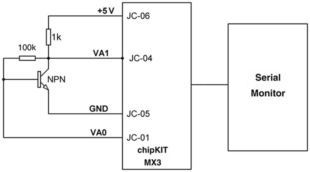
FIGURE 7.94 Project Hardware
FIGURE 7.95 Hardware Setup
7.20.3. Project PDL
The operation of the project is described in the PDL shown in Figure 7.96. At the beginning of the program, the Serial Monitor interface is initialised to 9600 Baud. A heading is displayed, and the ADC reference voltage is set to INTERNAL. The program then reads the base and collector analogue voltages, calculates the various currents and voltages in the circuit, and then displays them on the Serial Monitor.
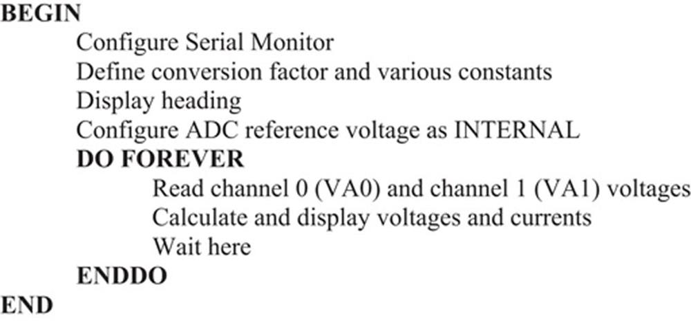
FIGURE 7.96 PDL of the Project
7.20.4. Project Program
The program is called NPN, and the program listing is shown in Figure 7.97. At the beginning of the program, various constants used in the program are declared. Then, the Serial Monitor is configured to operate at 9600 Baud. Inside the main program loop, all the required voltages and currents are calculated using the formulas given earlier and displayed via the Serial Monitor.
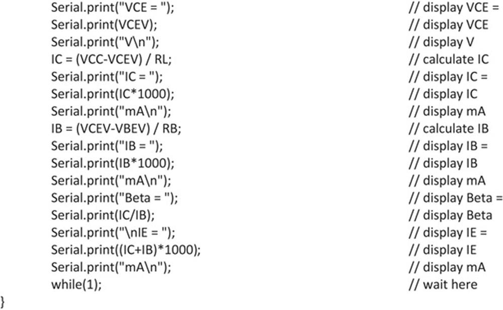
FIGURE 7.97 Program Listing
Figure 7.98 shows a typical output from the program (in this example, a BC108-type NPN transistor was used).
FIGURE 7.98 A Typical Output From the Program
7.21. Project 7.21 – Writing to SD Card
7.21.1. Project Description
In this and the next few projects, we will be using SD cards as storage devices. But before going into the details of these projects, we should take a look at the basic principles and operation of SD card memory devices.
SD cards are commonly used in many electronic devices where large amount of nonvolatile data storage is required. Some application areas are:
• Digital cameras
• Camcorders
• Printers
• Laptop computers
• Global Positioning System (GPS) receivers
• Electronic games
• PDAs
• Mobile phones
• Embedded electronic systems
Figure 7.99 shows the picture of a typical SD card.
FIGURE 7.99 A Typical SD Card
The SD card is a flash memory storage device designed to provide high-capacity, nonvolatile, and rewritable storage in small size. The memory capacities of the SD cards are increasing all the time. Currently, they are available in capacities from several gigabytes to over 128 GB. SD cards are in three sizes: standard SD card, miniSD card, and the microSD card. Table 7.6 lists the main specifications of different size cards.
Table 7.6
Different size SD card specifications.
|
Standard SD |
miniSD |
microSD |
|
|
Dimensions (mm) |
32 × 24 × 2.1 |
21.5 × 20 × 1.4 |
15 × 11 × 1 |
|
Card weight (g) |
2.0 |
0.8 |
0.25 |
|
Operating voltage (V) |
2.7–3.6 |
2.7–3.6 |
2.7–3.6 |
|
Write protect |
Yes |
No |
No |
|
Pins |
9 |
11 |
8 |
|
Interface |
SD or SPI |
SD or SPI |
SD or SPI |
|
Current consumption (mA) |
100 (write) |
100 (write) |
100 (write) |
SD card specifications are maintained by the SD Card Association that has over 600 members. MiniSD and microSD cards are electrically compatible with the standard SD cards, and they can be inserted in special adapters and used as standard SD cards in standard card slots.
SD card speeds are measured in three different ways: in kilobytes per second, in megabytes per second, or in an “x” rating similar to that of CD-ROMS, where “x” is the speed corresponding to 150 KB/s. Thus, the various “x”-based speeds are:
• 4x: 600 KB/s
• 16x: 2.4 MB/s
• 40x: 6.0 MB/s
• 66x: 10 MB/s
As far as the memory capacity is concerned, we can divide SD cards into three families: Standard-Capacity (SDSC), High-Capacity (SDHC), and eXtended-Capacity (SDXC). SDSC are the older cards with capacities 1–2 GB. SDHC have capacities 4–32 GB, and SDXC cards have capacities greater than 32–128 GB. The SD and SDHC families are available in all three sizes, but the SDXC family is not available in the mini size.
In the projects in this book, we shall be using the standard SD cards only. The use of smaller-size SD cards is virtually the same and is not described here any further.
SD cards can be interfaced with microcontrollers using two different protocols: SD card protocol and the Serial Peripheral Interface (SPI) protocol. The SPI protocol is the most commonly used protocol and is the one used in the projects in this book. SPI bus is currently used by microcontroller interface circuits to talk to a variety of devices such as:
• Memory devices (SD cards)
• Sensors
• Real-time clocks
• Communications devices
• Displays
The advantages of the SPI bus are:
• Simple communication protocol
• Full duplex communication
• Very simple hardware interface
In addition, the disadvantages of the SPI bus are:
• Requires four pins
• No hardware flow control
• No slave acknowledgement
It is important to realise that there are no SPI standards governed by any international committee. As a result of this, there are several versions of the SPI bus implementation. In some applications, two data lines are combined into a single data line, thus reducing the line requirements into three. Some implementations have two clocks, one to capture (or display) data and another to clock it into the device. Also, in some implementations, the chip select line may be active-high rather than active-low.
The standard SD card has nine pins with the pin layout shown in Figure 7.100. Depending on the interface protocol used, pins have different functions. Table 7.7 gives the function of each pin both in SD mode and in SPI mode of operation.
FIGURE 7.100 Standard SD Card Pin Layout
Table 7.7
Standard SD card pin definitions.
|
Pin |
Name |
SD Description |
SPI Description |
|
1 |
CD/DAT3/CS |
Data line 3 |
Chip select |
|
2 |
CMD/Datain |
Command/response |
Host to card command and data |
|
3 |
VSS |
Supply ground |
Supply ground |
|
4 |
VDD |
Supply voltage |
Supply voltage |
|
5 |
CLK |
Clock |
Clock |
|
6 |
VSS2 |
Supply voltage ground |
Supply voltage ground |
|
7 |
DAT0 |
Data line 0 |
Card to host data and status |
|
8 |
DAT1 |
Data line 1 |
Reserved |
|
9 |
DAT2 |
Data line 2 |
Reserved |
Before going into details of the SD card projects, it is worthwhile to look at the operation of the SPI bus briefly.
Figure 7.101 shows a simplified block diagram of an SPI bus implementation with a master and three slave devices communicating over the SPI bus. In this figure, the slaves are selected by the slave select (SS) signals generated by the master. The clock and data lines are common to all the devices.
FIGURE 7.101 A Master and Three Slave Devices on the SPI Bus
7.21.2. chipKIT MX3 SPI Signals
The PIC32 microcontroller contains two SPI bus interfaces named SPI1 and SPI2. The SPI bus signals on the PIC32 are labelled as SS, serial data out (SDO), serial data in (SDI), and serial clock (SCL).
SPI1 is accessed via Pmod connector JB, and SPI2 is accessed via Pmod connector JE. The SPI bus interface pins are:
• JB-01: RD9 (used for SS output)
• JB-02: SDO1
• JB-03: SDI1
• JB-04: SCL1
• JE-01: SS2
• JE-02: MOSI
• JE-03: MISO
• JE-04: SCL2
SPI1 supports SPI master, but it can also be used as SPI slave by using external wiring, and when used as a slave, the SS1 signal is obtained from Pmod connector JD-01.
SPI2 can be used as an SPI master or slave. Jumpers JP6 and JP8 are used to select between master and slave by switching the microcontroller signals SDO2 and SDI2 between the SPI signals MOSI and MISO at the Pmod connector (M position for SPI master operation and S position for SPI slave operation).
The chipKIT SPI library or the Digilent DSPI library can be used to access the SPI bus when using the MPIDE development environment. The chipKIT library supports the SPI2 interface, while the DSPI library supports both SPI1 and SPI2 ports.
The SD card library (sd.h) distributed with the MPIDE development system uses the software-implemented SPI library with the following connections:
• JC-01: SS
• JC-02: SDO
• JC-03: SDI
• JC-04: SCL
7.21.3. Operation of the SD Card in SPI Mode
When the SD card is operated in SPI mode, only seven pins are used:
• Two power supply ground (pins 3 and 6)
• Power supply (pin 4)
• Chip select (pin 1)
• Data out (pin 7)
• Data in (pin 2)
• CLK (pin 5)
Three pins are used for the power supply, leaving four pins for the SPI mode of operation:
• Chip select (pin 1)
• Data out (pin 7)
• Data in (pin 2)
• CLK (pin 5)
At power-up, the SD card defaults to the SD bus protocol. The card is switched to the SPI mode if the CS signal is asserted during the reception of the reset command. When the card is in SPI mode, it only responds to SPI commands. The host may reset a card by switching the power supply off and on again.
Most high-level language compilers normally provide a library of commands for initialising, reading, and writing to SD cards. In general, it is not necessary to know the internal structure of an SD card before it can be used since the available library functions can easily be used. It is, however, important to have some knowledge about the internal structure of an SD card so that it can be used efficiently. In this section, we shall be looking briefly at the internal architecture and the operation of SD cards.
An SD card has a set of registers that provide information about the status of the card. When the card is operated in SPI mode, these registers are:
• Card Identification Register (CID)
• Card-Specific Data Register (CSD)
• SD Configuration Register (SCR)
• Operation Control Register (OCR)
The CID register consists of 16 bytes, and it contains the manufacturer ID, product name, product revision, card serial number, manufacturer date code, and a checksum byte.
The CSD register consists of 16 bytes, and it contains card-specific data such as the card data transfer rate, R/W block lengths, R/W currents, erase sector size, file format, write protection flags, checksum, etc.
The SCR register is 8 bytes long, and it contains information about the SD card’s special features and capabilities such as the security support, data bus widths supported, etc.
The OCR register is only 4 bytes long, and it stores the VDD voltage profile of the card. The OCR shows the voltage range in which the card data can be accessed.
All SD card SPI commands are 6 bytes long with the MSB transmitted first. First byte is known as the “command” byte, and the remaining 5 bytes are “command arguments.” Bit 6 of the command byte is set to “1,” and the MSB bit is always “0.” With the remaining 6 bits, we have 64 possible commands, named CMD0–CMD63. Some of the important commands are:
• CMD0: GO_IDLE_STATE (resets the SD card)
• CMD1: SEND_OP_COND (initialises the card)
• CMD9: SEND_CSD (gets CSD register data)
• CMD10: SEND_CID (gets CID register data)
• CMD16: SET_BLOCKLEN (selects a block length in bytes)
• CMD17: READ_SINGLE_BLOCK (reads a block of data)
• CMD24: WRITE_BLOCK (writes a block of data)
• CMD32: ERASE_WR_BLK_START_ADDR (sets the address of the first write block to be erased)
• CMD33: ERASE_WR_BLK_END_ADDR (sets the address of the last write block to be erased)
• CMD38: ERASE (erases all previously selected blocks)
In response to a command, the card sends a status byte known as R1. The MSB bit of this byte is always “0,” and the other bits indicate various error conditions.
Reading data
SD card in SPI mode supports single block and multiple block read operations. The host should set the block length, and after a valid read command the card responds with a response token, followed by a data block, and a cyclic redundancy check (CRC). The block length can be between 1 and 512 bytes. The starting address can be any valid address range of the card.
In multiple block read operations, the card sends data blocks with each block having its own CRC attached to the end of the block.
Writing data
SD card in SPI mode supports single or multiple block write operations. After receiving a valid write command from the host, the card will respond with a response token, and will wait to receive a data block. A 1-byte “start block” token is added to the beginning of every data block. After receiving the data block, the card responds with a “data response” token and the card will be programmed as long as the data block has been received with no errors.
In multiple write operations, the host sends the data blocks one after the other, each preceded with a “start block” token. The card sends a response byte after receiving each data block.
A card can be inserted and removed from the bus without any damage. This is because all data transfer operations are protected by CRC codes and any bit changes as a result of inserting or removing a card can easily be detected. SD cards operate with a typical supply voltage of 2.7 V. The maximum allowed power supply voltage is 3.6 V. If the card is to be operated from a standard 5.0 V supply, a voltage regulator should be used to drop the voltage to 2.7 V.
Using an SD card requires the card to be inserted into a special card holder with external contacts (see Figure 7.102). Connections can then be made easily to the required card pins.
FIGURE 7.102 SD Card Holder
In this project, a file called MYFILE.TXT is created on the SD card and the following text is written to the file:
This book is about the chipKIT MX3 development board.
The book gives the features of this development board.
In addition, many projects are given in the book.
The block diagram of the project is shown in Figure 7.103.
FIGURE 7.103 Block Diagram of the Project
7.21.4. Project Hardware
The Pmod module PmodSD is used in this project. As shown in Figure 7.104, PmodSD is a 2 × 6 pin module with a standard size SD card holder. The connection diagram of this module is shown in Figure 7.105.
When used in SPI data mode, only the pins at the top row (1–6) are used. The WP signal (pin 10) is the optional write protect and can be set by a switch on the SD card to prevent writing or erasing the card accidentally. The CD signal (pin 9) is optional and can be used by the microcontroller to indicate that a card is in the SD card slot.
In this project, the PmodSD module is connected to Pmod connector JC (see Figure 7.106). Therefore, the interface between the PmodSD module and the development board is as follows (notice that JC-01 is at logical I/O port number 16):
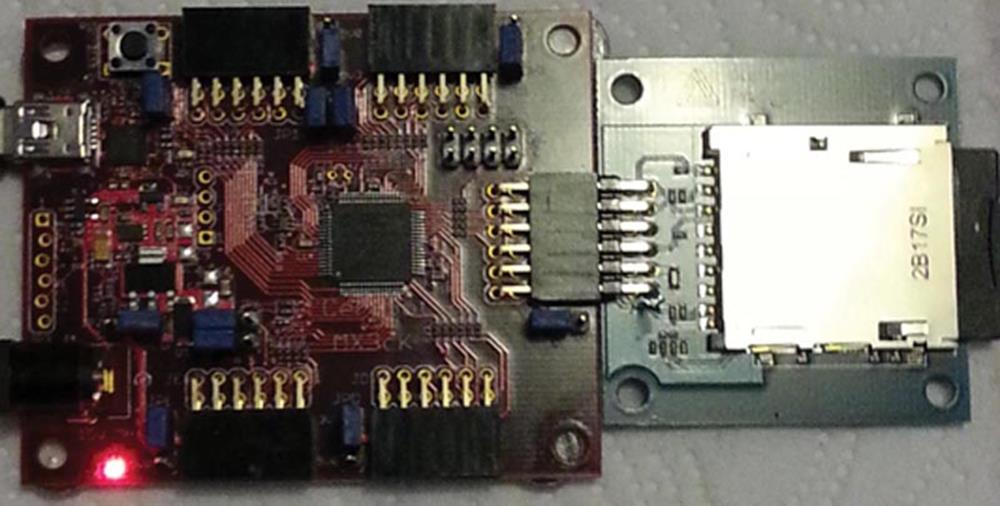
FIGURE 7.106 Hardware Setup
|
Pmod JPC Connector |
SPI Signal Name |
SD Card SPI Signal |
|
JC-01 |
SS |
CS |
|
JC-02 |
SDO |
DI |
|
JC-03 |
SDI |
DO |
|
JC-04 |
SCL |
CLK |
Figure 7.107 shows the circuit diagram of the project (notice that LEDs LD4 and LD5 are not shown in this figure as they are mounted on the chipKIT MX3 board).
7.21.5. Project PDL
Before looking at the programming details, it is worthwhile to see what type of SD card library functions are available for managing SD card–based applications. A brief summary of the commonly used SD card library functions is given below.
The SD card library supports both FAT16 and FAT32 file systems on standard SD and SDHC cards. Files can have names made up of up to 8 characters, followed by an extension made up of 3 characters (8.3 file naming convention).
SD.begin(cs): This function initialises the SD card library. The cs is optional and defaults to the SS line for the hardware SPI bus. The function returns True on success and False on failure.
SD.exists(filename): This function checks to see whether or not the specified file exists in the current directory. The forward slash character “/” can be used to look for the file in a directory. The function returns a True if file exists, or False if the file does not exist.
SD.mkdir(name): This function creates a folder on the SD card with the specified name. A subdirectory can be specified using forward slashes. A True is returned if the requested directory is created; otherwise, a False is returned.
SD.remove(filename): This function deletes the specified file on the SD card. A True is returned if the file is removed successfully; otherwise, a False is returned.
SD.rmdir(name): This function deletes a directory on the SD card. The directory must be empty before it can be removed. A True is returned if the operation is successful; otherwise, a False is returned.
SD.open(filename, mode): This function opens an existing file on the SD card. If the file does not exist, then a new file with the specified name will be created. Notice that the filename can contain directory names if required. The directory names must be specified using the forward slash character. Mode specifies whether the file will be opened for reading or writing. FILE_READ opens the file for reading, and the file pointer is positioned at the beginning of the file. FILE_WRITE opens the file for reading and writing. If the file exists, then the file pointer is positioned at the end of the file.
file.close(): This function writes any remaining data to the file and closes the file. file is an instance of the file class returned by SD.open().
file.read(): This function is used to read a byte (next byte) from the file. file is an instance of the file class returned by SD.open().
file.available(): This function checks if there are any bytes available for reading from the file. The number of bytes available for reading is returned as an integer. file is an instance of the file class returned by SD.open().
file.write(data): This function is used to write a byte to the already opened file. file is an instance of the file class returned by SD.open().
file.write(buffer, len): This function is used to write an array of characters of length len to the file. file is an instance of the file class returned by SD.open(). The number of bytes written to the file is returned as a byte.
file.flush(): This function ensures that all the bytes belonging to the file are physically written to the file (the close function automatically flushed the data before closing the file).
file.position(): This function returns (as an unsigned long) the position of the next location in the file where data is to be written to or read from. file is an instance of the file class returned by SD.open().
file.size(): This function returns the size of the file in bytes. file is an instance of the file class returned by SD.open().
file.print(data): This function writes data to the file. The data can be byte, integer, long, or string. file is an instance of the file class returned by SD.open(). An optional BASE parameter can be used to specify the base of the number to be printed. Valid BASE parameters are BIN (binary), DEC (decimal), OCT (octal), or HEX (hexadecimal). The number of bytes written to the file is returned by the function.
file.println(data): This function is similar to file.print(data), but here newline characters (carriage return and line feed) are also written to the file.
Figure 7.108 shows the PDL of the project. At the beginning, the chip select is configured as logical I/O port number 16 (JC-01). Then the two on-board LEDs LD4 and LD5 are configured as outputs. These LEDs are used to indicate error conditions. The SD card library is then started. If there is an error in starting the library, then LD4 is turned ON and the program stops. Otherwise, file MYFILE.TXT is created on the SD card and the following text is written inside this file. If the file cannot be opened, then both LD4 and LD5 are turned ON to indicate an error condition:
This book is about the chipKIT MX3 development board.
The book gives the features of this development board.
In addition, many projects are given in the book.
7.21.6. Project Program
The header file sd.h must be included at the beginning of a program that uses the SD card library. The program is called FILEW, and the program listing is shown in Figure 7.109. At the beginning of the program, the chip select pin (logical I/O port number 16) and the LD4 (logical I/O port number 42) and LD5 (logical I/O port number 43) are configured as outputs. The remainder of the program is executed inside the setup() routine. Here, both LEDs are turned OFF initially to indicate that there are no errors to start with. Then, the SD card library is initialised by calling function SD.begin(). If there is an error in initialising this library, then LD4 is turned ON and the program stops. Otherwise, file MYFILE.TXT is created on the SD card and the required text is written inside this file. If the file cannot be opened, then both LEDs LD4 and LD5 are turned ON to indicate the error condition.
Figure 7.110 shows contents of file MYFILE.TXT displayed on the PC using the Notepad program after inserting the card to the PC via an SD card reader.
FIGURE 7.110 Contents of File MYFILE.TXT
7.22. Project 7.22 – Reading From SD Card and Displaying on Serial Monitor
7.22.1. Project Description
This project is similar to the previous one, but here the file MYFILE.TXT created in the previous project is opened for reading and its contents are displayed on the Serial Monitor.
The block diagram of the project is shown in Figure 7.111.
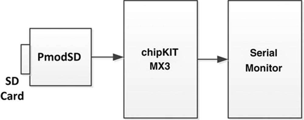
FIGURE 7.111 Block Diagram of the Project
7.22.2. Project Hardware
As in the previous project, the PmodSD module is connected to Pmod connector JPC (see Figures 7.106 and 7.107).
7.22.3. Project PDL
The project PDL is shown in Figure 7.112. At the beginning, the chip select is configured as logical I/O port number 16 (JC-01), and Serial Monitor is also initialised. The SD card library is then started. If there is an error in starting the library, then an appropriate message is sent to the Serial Monitor and the program stops. Otherwise, file MYFILE.TXT is opened for reading and its contents are read and displayed on the Serial Monitor. If the file cannot be opened, then an appropriate message is sent to the Serial Monitor.
7.22.4. Project Program
The program is called FILER, and the program listing is shown in Figure 7.113. At the beginning of the program, the chip select pin (logical I/O port number 16) is configured as output, and Serial Monitor is initialised to operate at 9600 Baud. The remainder of the program is executed inside the setup() routine. Here, the SD card library is initialised, file MYFILE.TXT is opened for reading, and the contents of this file are displayed on the Serial Monitor.
Figure 7.114 shows the Serial Monitor displaying contents of the file.
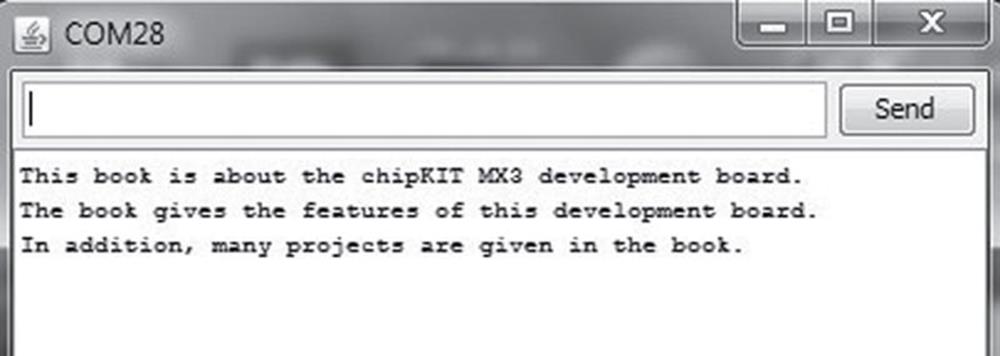
FIGURE 7.114 The Serial Monitor
7.23. Project 7.23 – Temperature Data Logging on SD Card
7.23.1. Project Description
This project measures the ambient temperature as in Project 7.19. In this project, the temperature is read every 5 s and is stored on an SD card in a file called TEMPS.TXT. The program runs for 1 min where 12 records are written to the file.
The block diagram of the project is shown in Figure 7.115. As in Project 7.19, the temperature sensor chip LM35DZ is used in this project. LM35DZ is a three-pin temperature sensor chip whose output voltage is proportional to the ambient temperature and is given by: Vo = 10 mV/°C. Thus, for example, at 20°C the output voltage is 200 mV, at 30°C the output voltage is 300 mV, and so on.
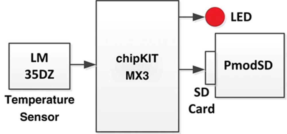
FIGURE 7.115 Block Diagram of the Project
7.23.2. Project Hardware
As in Project 7.22, the PmodSD module is connected to Pmod connector JC (see Figures 7.106 and 7.107). When using the MPIDE development environment with the PIC32 microcontrollers, the available analogue input channels are given as in the following table:
|
Analogue Channel |
Pmod Connector |
Digital Pin Number |
Microcontroller Pin |
|
A0 |
JC-01 |
16 |
RB8 |
|
A1 |
JC-04 |
19 |
RB14 |
|
A2 |
JC-07 |
20 |
RB0 |
|
A3 |
JC-08 |
21 |
RB1 |
|
A4 |
JD-01 |
24 |
RB2 |
|
A5 |
JD-04 |
27 |
RB9 |
|
A6 |
JD-07 |
28 |
RB12 |
|
A7 |
JD-10 |
31 |
RB13 |
|
A8 |
JE-08 |
37 |
RB5 |
|
A9 |
JE-09 |
38 |
RB4 |
|
A10 |
JE-10 |
39 |
RB3 |
Because Pmod connector JC is used for the SD card, the output of the temperature sensor chip is connected to analogue port A4 (Pmod connector JD-01). The Pmod breadboard module PmodBB is used to interface to the LM35DZ temperature sensor chip.
Figure 7.116 shows the project hardware setup. The circuit diagram of the project is shown in Figure 7.117 (LED LD4 is not shown here since it is on the chipKIT MX4 board).
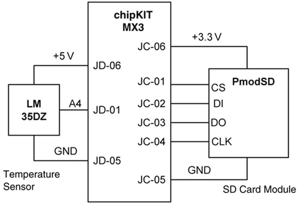
FIGURE 7.117 Circuit Diagram of the Project
7.23.3. Project PDL
The project PDL is shown in Figure 7.118. At the beginning, the chip select is configured as logical I/O port number 16 (JC-01) and the analogue-to-digital conversion factor is declared. The SD card library is then started. If there is an error in starting the library, then LED LD4 is turned ON and the program stops. Otherwise, file TEMPS.TXT is created and the temperature is written to the file every 5 s. The data is recorded for up to 1 min (i.e., 12 records), and after this time the file is closed and the program stops. If the file cannot be created, then the LED LD4 is turned ON to indicate the error condition.
7.23.4. Project Program
The program is called LOGGER, and the program listing is shown in Figure 7.119. At the beginning of the program, the chip select pin (logical I/O port number 16) is configured as an output. The SD card library is started using SD library function SD.begin(). If the library is started successfully, then file TEMPS.TXT is created on the SD card and the heading TEMPERATURE DATA LOGGER is written to the file. The program then reads the temperature every 5 s and writes it to the file. This process continues for 1 min where a total of 12 records are written to the file.
Figure 7.120 shows the contents of file TEMPS.TXT displayed on the PC using the Notepad program.
7.24. Project 7.24 – Generating Sound Using a Buzzer
7.24.1. Project Description
This project uses a small piezoelectric buzzer to generate sound. In this project, the SOS Morse code (…---…) is output from the buzzer, where the sound frequency is set to 440 Hz. The basic dot duration is set to 150 ms.
The block diagram of the project is shown in Figure 7.121.
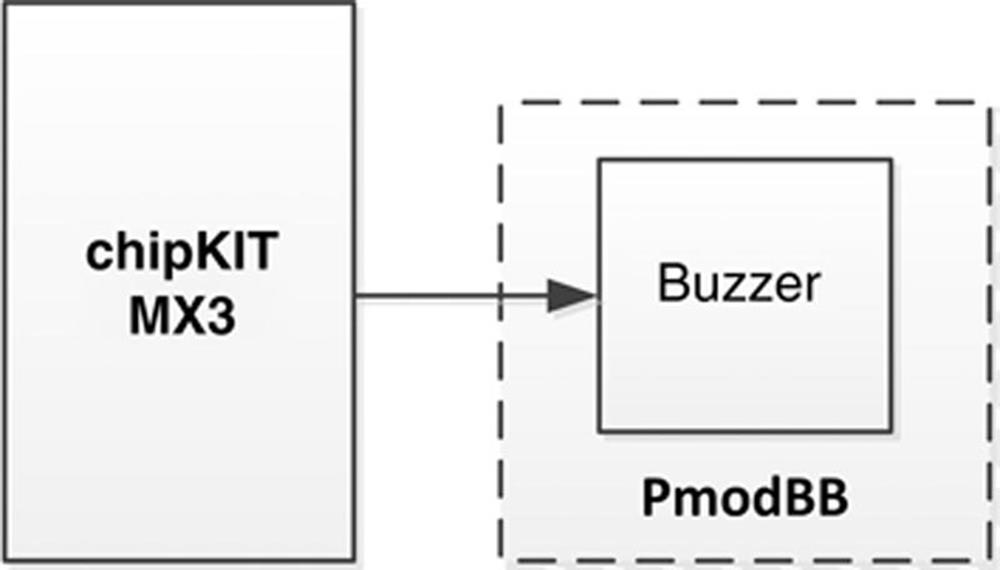
FIGURE 7.121 Block Diagram of the Project
The Morse code dot and dash timings are as follows:
• Basic unit is the dot time.
• Dash time is three times the dot time.
• The gap between dots and dashes is equal to one dot time.
• The gap between letters is equal to three dot times.
• The gap between words is seven dot times.
7.24.2. Project Hardware
As shown in the circuit diagram in Figure 7.122, a small piezoelectric buzzer is connected to logical port pin 0 (Pmod connector JA-01) through a switching transistor. The buzzer sounds when the transistor is turned ON.
The MPIDE built-in sound functions tone() and noTone() are used in this project. As mentioned earlier, the tone(pin, frequency, duration) function has three arguments. The first argument is the pin number used, second argument is the frequency of the tone to be generated (in Hz), and duration is the tone duration (in milliseconds). The duration is optional and can be omitted if desired. Function noTone() has no arguments, and calling this function stops generating tone.
The PDL of the project is shown in Figure 7.123. In this project, the piezoelectric buzzer is connected to logical port number 0 (Pmod connector JA-01) using the PmodBB breadboard module. The program configures the port as output and then calls to functions called DOTS and DASHES to generate the required SOS sound on the buzzer.
7.24.4. Project Program
The program is called SOS, and the program listing is shown in Figure 7.124. At the beginning of the program, logical port 0 is configured as output. Inside the main program, functions DOTS and DASHES are called to generate the three dots and three dashes for the SOS signal. Function DOTS generates three short tones with durations equal to the basic dot time. Similarly, function DASHES generates three short notes with durations equal to three dot times.
7.25. Project 7.25 – Generating Melody Using a Buzzer
7.25.1. Project Description
This project shows how sound with different frequencies can be generated using a simple buzzer. The project shows how the simple melody Happy Birthday can be played using a buzzer.
The block diagram of the project is same as in Figure 7.121.
7.25.2. Project Hardware
The project hardware is same as in Figure 7.122.
7.25.3. Project PDL
When playing a melody, each note is played for a certain duration and with a certain frequency. In addition, a certain gap is necessary between two successive notes. The frequencies of the musical notes starting from middle C (i.e., C4) are given below. The harmonic of a note is obtained by doubling the frequency. For example, the frequency of C5 is 2 × 262 = 524 Hz.
|
Notes |
C4 |
C4# |
D4 |
D4# |
E4 |
F4 |
F4# |
G4 |
G4# |
A4 |
A4# |
B4 |
|
Frequency (Hz) |
261.63 |
277.18 |
293.66 |
311.13 |
329.63 |
349.23 |
370 |
392 |
415.3 |
440 |
466.16 |
493.88 |
In order to play the tune of a song, we need to know its musical notes. Each note is played for certain duration, and there is a certain time gap between two successive notes.
In this project, we will be generating the classic Happy Birthday melody and thus we need to know the notes and their durations. These are given in the following table where the durations are in milliseconds and should be multiplied by 400 to give correct values:
|
Note |
C4 |
C4 |
D4 |
C4 |
F4 |
E4 |
C4 |
C4 |
D4 |
C4 |
G4 |
F4 |
C4 |
C4 |
C5 |
A4 |
F4 |
E4 |
D4 |
A4# |
A4# |
A4 |
F4 |
G4 |
F4 |
|
Duration |
1 |
1 |
2 |
2 |
2 |
3 |
1 |
1 |
2 |
2 |
2 |
3 |
1 |
1 |
2 |
2 |
2 |
2 |
2 |
1 |
1 |
2 |
2 |
2 |
4 |
The PDL of the project is shown in Figure 7.125. Basically two tables are used to store the notes and their corresponding durations. Then the tone() function is called in a loop to play all the notes. The melody repeats after 3-s delay.
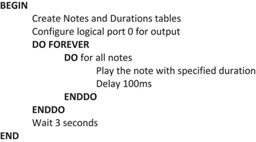
FIGURE 7.125 PDL of the Project
7.25.4. Project Program
The program is called MELODY, and its listing is given in Figure 7.126. At the beginning of the program, logical port 0 is configured for output and tables Notes and Durations store the frequencies (Hz) and durations (1/400 ms) of each note, respectively. Inside the main program loop, each note is played with the specified duration. A 100-ms gap is used between each note. The durations and the gap can be changed to increase or decrease the speed of the melody.
7.26. Project 7.26 – Using an Audio Amplifier
7.26.1. Project Description
This project is similar to Project 7.25, but here an audio amplifier is used to amplify the tones and output on a speaker.
Buzzers are normally used as alarm warning devices, and they do not produce tones at different frequencies. In this project, an audio amplifier is used to generate good-quality tones for our melody.
The block diagram of the project is shown in Figure 7.127.
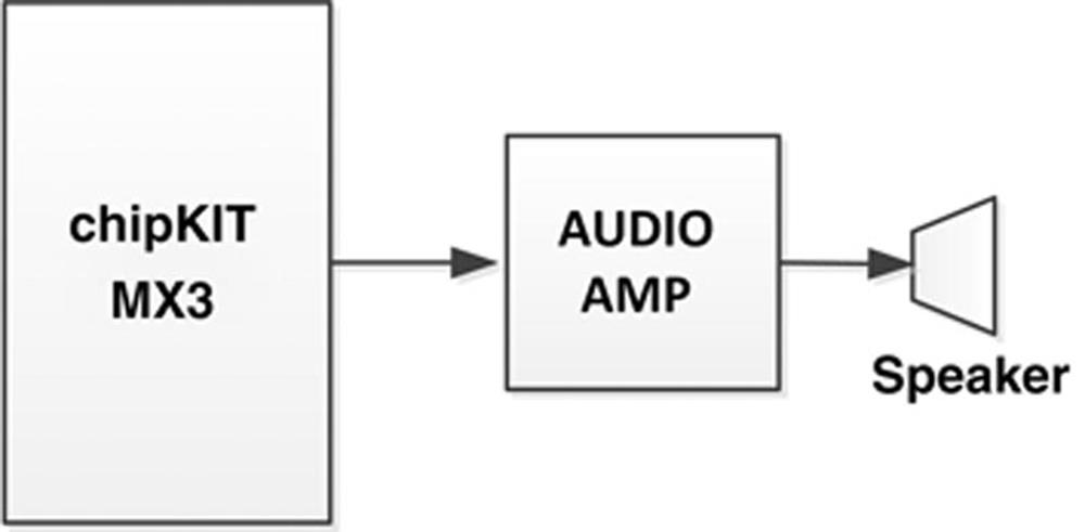
FIGURE 7.127 Block Diagram of the Project
7.26.2. Project Hardware
In this project, the audio amplifier module called AUDIO AMP manufactured by mikroElektronika (www.mikroe.com) is used. As shown in Figure 7.128, this is a small audio amplifier board that operates with +5 V supply. Audio signal is fed from one end of the board through a pair of screw-type connectors. The output of the amplifier board is connected to a speaker for high-volume and high-quality sound output.
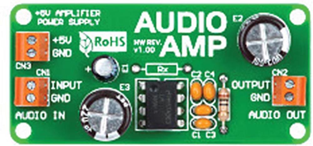
FIGURE 7.128 The mikroElektronika Audio Amplifier Board
The audio amplifier board uses an LM386-type audio amplifier chip, and its circuit diagram is shown in Figure 7.129.
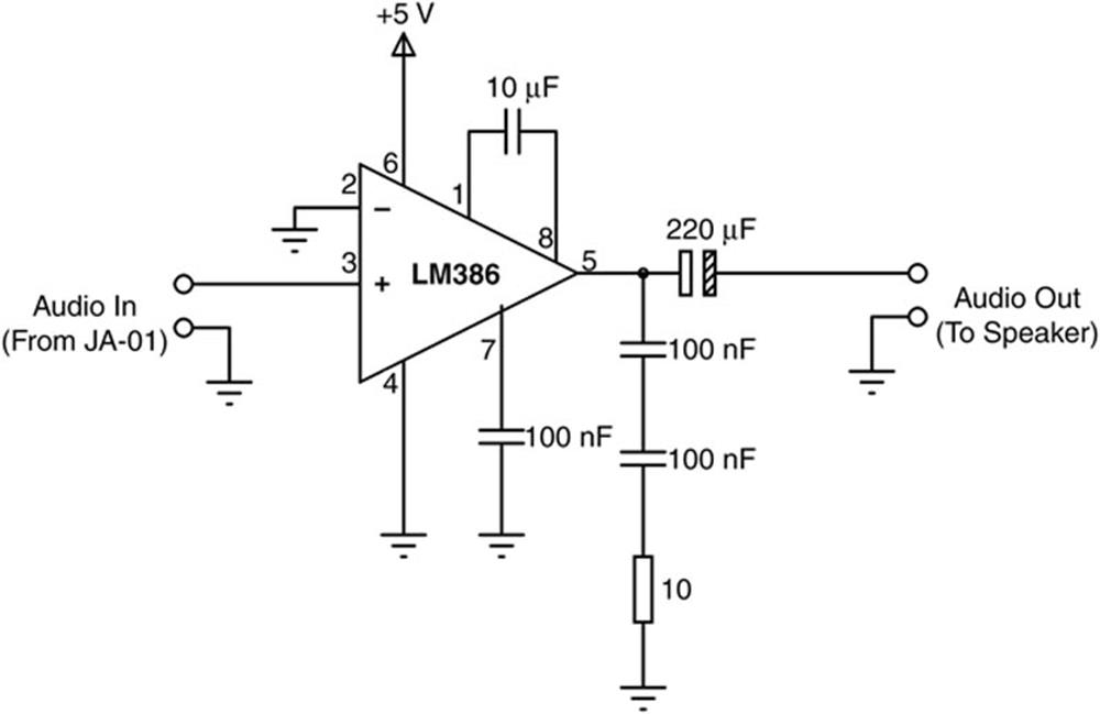
FIGURE 7.129 Circuit Diagram of the Audio Amplifier
Pmod connector power jumper is set to +5 V, and power is applied from pins JA-05 and JA-06 to the audio amplifier board. Pin JA-01 of the Pmod connector is connected to the audio input of the amplifier board. Figure 7.130 shows the hardware setup of the project.
The basic features of the audio amplifier board used in this project are as follows:
• LM386 audio power amplifier
• +5 V operation
• Easy connectivity using provided input and output screw terminals
The project PDL and project program are same as in Figures 7.125 and 7.126, respectively.
7.27. Project 7.27 – Waveform Generation: Using DAC
7.27.1. Project Description
Waveform generation is very important in digital signal processing. In this project, we will be seeing how to generate simple waveforms using a digital-to-analogue converter (DAC) module.
Figure 7.131 shows the block diagram of a typical microcontroller-based waveform generation system. Here, the microcontroller generates the required waveform as a digital signal and then the DAC converts this signal into analogue. In practical applications, a low-pass filter is used after the DAC to clean the signal and remove any high-frequency components.
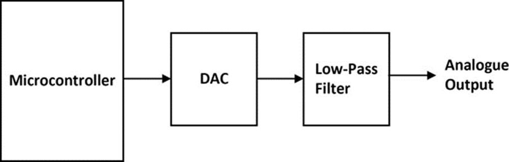
FIGURE 7.131 Block Diagram of Microcontroller-Based Waveform Generation
Basically two methods are used for waveform generation:
• The microcontroller calculates the waveform points in real time and sends them to the DAC.
• The waveform points are stored in a look-up table. The microcontroller reads these points from the table and sends them to the DAC (this method is used to generate any arbitrary waveform, or to generate higher-frequency waveforms).
As we shall see later, the rate at which the waveform points are sent to the DAC determines the frequency of the waveform.
Before going into the details of actually generating waveforms, it is worthwhile to look at the operation of a typical DAC. There are several forms of DACs available in the market. In this project, we will be using the R2R-type DAC that simply consists of resistors. The DAC we will be using in this project is the Pmod peripheral module PmodR2R, and it provides 8-bit conversion with up to 25 MHz operation. R2R-type DAC converters are cheap as they consist of only resistors and they are also fast.
Figure 7.132 shows a picture of the PmodR2R module. The connection diagram of the module is shown in Figure 7.133.
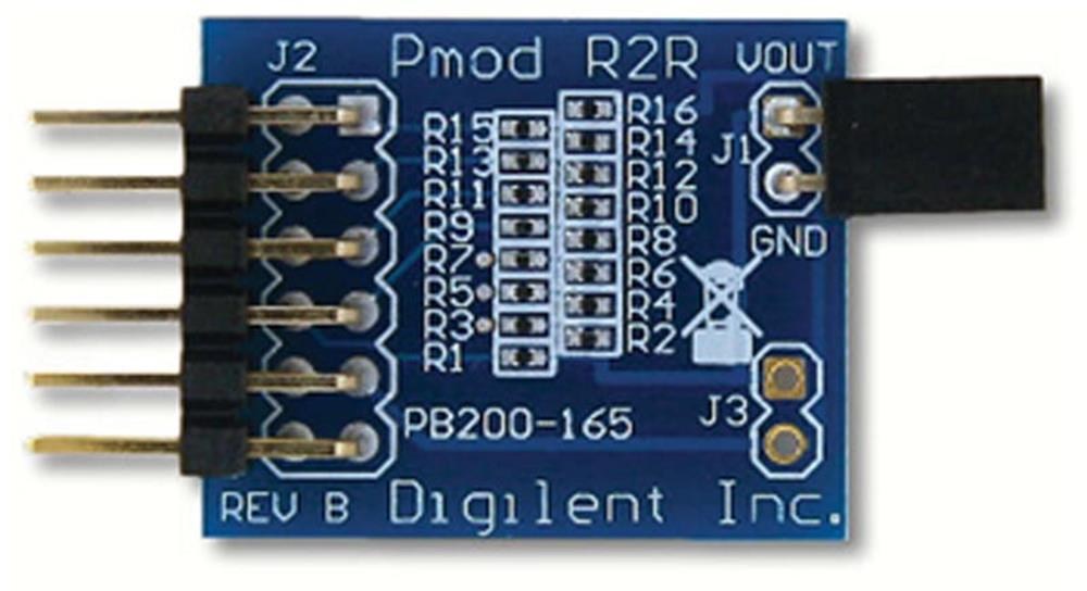
FIGURE 7.132 The PmodR2R DAC Module
The PmodR2R module contains a 2 × 6 connector, and it can be connected to any of the Pmod connectors on the chipKIT MX3 development board. The converted analogue signal is available on header J1.
For a digital value D, of a R2R DAC, the output voltage is given by:
The PmodR2R is 8-bit wide and, therefore, N = 8, 2N = 256. With Vref = 3.3 V (typical CMOS logic HIGH voltage), Vout will be:

For D = 1, we have

For D = 255, we have

Thus, the output voltage of the DAC changes from 0 to +3.28 V and the step size is 12.89 mV.
7.27.2. Project Hardware
The PmodR2R DAC module is connected to Pmod connector JA. Thus, the connection between the DAC module and the logical I/O ports is as follows:
|
PmodR2R Pin |
Logical I/O Port |
JA Connector Pin |
|
D0 |
0 |
JA-01 |
|
D1 |
1 |
JA-02 |
|
D2 |
2 |
JA-03 |
|
D3 |
3 |
JA-04 |
|
D4 |
4 |
JA-07 |
|
D5 |
5 |
JA-08 |
|
D6 |
6 |
JA-09 |
|
D7 |
7 |
JA-10 |
Figure 7.134 shows the hardware setup. The circuit diagram of the project is shown in Figure 7.135.
Generating square waveform
In general, a square waveform with an amplitude equal to logic 1, that is, about +3.3 V (or +5 V) at audio frequencies can easily be generated by toggling an output pin of the microcontroller. In this section, we shall be using the DAC to generate a square waveform with an amplitude of +1.0 V and period of 10 ms, with a duty cycle of 50%, that is, 5 ms ON time and 5 ms OFF time.
The required program listing is shown in Figure 7.136. Logical port numbers 0–7 are configured as outputs. Then, for 1 V output, the data to be sent to the port is:
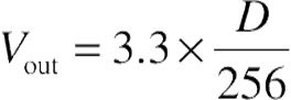
or
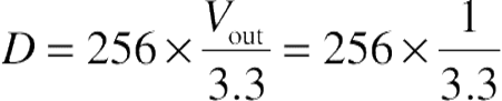
or
![]()
Inside the main program loop, decimal number 77 is sent to the port and the port state is toggled every 5 ms so that the period of the square waveform is 10 ms. Array PmodDAC stores the logical I/O port numbers for the port at connector JA. These port pins are configured as output inside the setup() routine. In addition, the bit pattern of number 77 is found and stored in an array called Bits. Inside the main program loop, the bits are sent to the port pins for 5 ms. After this, the port pins are returned to 0 for 5 ms and this process is repeated, thus generating the required square wave. Function port converts a given byte into its bits and stores these bits in array Bits, where Bits[0] corresponds to the LSB bit and Bits[7] corresponds to the MSB bit.
FIGURE 7.137 The Generated Waveform
The program given in Figure 7.136 can be simplified by noticing that the pins JA-01 to JA-10 actually constitute PORTE of the microcontroller. Thus, we can send a byte directly to PORTE. The modified and simpler program is shown in Figure 7.138.
Generating sawtooth waveform
In this part of the project, we will be generating sawtooth waveform with the following specifications:
Output voltage: 0 to +3.3 V
Frequency: 100 Hz (period: 10 ms)
Step size: 0.1 ms
The block diagram and the circuit diagram of the project are as in the previous project. The PmodR2R module is connected to Pmod connector JA as before.
The program is called SAWTOOTH, and the program listing is given in Figure 7.139. At the beginning of the program, PORTE is configured as output. Inside the main program loop, the steps of the sawtooth waveform are sent out. Since there are 10 steps in the waveform and the required frequency is 100 Hz, that is, period 10 ms, the duration of each step should be 10,000/10 = 1000 μs. The delayMicroseconds() function is used to generate the required delay in microseconds.
Figure 7.140 shows the output waveform obtained using the PSCGU250 digital oscilloscope. Here the vertical axis is 1 V/division and the horizontal axis is 5 ms/division. The graph is moved down the 0 V point for clarity.
Generating sine waveform
In this part of the project, we will see how to generate a low-frequency sine wave using the built-in trigonometric sin function, and then send the output to the DAC. The generated sine wave has amplitude of ±1 V, frequency of 50 Hz, and D.C. offset of 2.0 V.
The frequency of the sine wave to be generated is 50 Hz. This wave has a period of 20 ms, or 20,000 μs. If we assume that the sine wave will consist of 100 samples, then each sample should be output at 20,000/100 = 200 μs intervals. The sample values will be calculated using the trigonometric sin function of the compiler.
The sin function will have the following format:

where T is the period of the waveform and is equal to 100 samples. Count is a variable that ranges from 0 to 100 and is incremented by 1 at each iteration. Thus, the sine wave is divided into 100 samples and each sample is output at 200 μs. The above formula can be rewritten as:
![]()
It is required that the amplitude of the waveform should be ±1 V. With a reference voltage of +3.3 V and an 8-bit R2R DAC converter, 1 V is equal to decimal number 77 (see previous project). Thus, we will multiply our sine function with the amplitude at each sample to give:
![]()
The DAC converter used in this project is unipolar and cannot output negative values. Therefore, a D.C. offset is added to the sine wave to shift it so that it is always positive. The offset should be larger than the absolute value of the maximum negative value of the sine wave, which is −77 when the sin function above is equal to −1. In this project, we wish to add 2.0 V D.C. offset, which corresponds to a decimal value of 155 at the DAC output. Thus, at each sample, we will calculate and output the following value to the DAC:
![]()
The program is called SINE, and its listing is shown in Figure 7.141. The sine wave amplitude is set to 77, offset is set to 155, and variable R is defined as 2π/100. The sine waveform values for a period are obtained in the setup() routine outside the main program loop. The reason for calculating these values outside the main program loop is to minimise the loop time so that higher-frequency sine waves can be generated. The sine values are calculated as follows:
for(i = 0; i < 100; i++)sins[i] = offset + Amplitude*sin(R*i);
Inside the main program, the sine samples are output with 200 μs delays so that the waveform has the required frequency.
Figure 7.142 shows the waveform generated by the program. It is clear from this figure that the generated sine waveform has period 20 ms as designed. Here, the vertical axis is 1 V/division and the horizontal axis is 5 ms/division.
7.28. Project 7.28 – Using a Keypad
7.28.1. Project Description
Keypads are small keyboards that are used to enter numeric or alphanumeric data to microcontroller systems. Keypads are available in a variety of sizes and styles from 2 × 2 to 4 × 4 or even bigger.
In this project, the PmodKYPD module is used. This is a 4 × 4 keypad with 2 × 6 pins and keys labelled 0–9 and A–F. Figure 7.143 shows a picture of the PmodKYPD module.
This is a simple project where the Serial Monitor displays the key pressed on the keypad.
7.28.2. Keypad Structure
Figure 7.144 shows the structure of a typical 4 × 4 keypad, consisting of 16 switches, formed in a 4 × 4 array. Assuming the keypad is connected to PORT C, the steps to detect which key is pressed are as follows:
• A logic 1 is applied to first column via RC0.
• Port pins RC4–RC7 are read. If the data is nonzero, then a switch is pressed. If RC4 is 1, key 1 is pressed; if RC5 is 1, key 4 is pressed; if RC6 is 1, key 9 is pressed; and so on.
• A logic 1 is applied to second column via RC1.
• Again port pins RC4–RC7 are read. If the data is nonzero, then a switch is pressed. If RC4 is 1, key 2 is pressed; if RC5 is 1, key 6 is pressed; if RC6 is 1, key 0 is pressed; and so on.
• The above process is repeated for all four columns continuously.
Table 7.8 shows the pin layout of the PmodKYPD module. Assuming that the keypad is connected to Pmod connector JA, the column and row numbers and corresponding I/O port logical names are shown in Table 7.9.
Table 7.8
PmodKYPD pin layout.
|
Connector J1 – Column/Row Indicators |
||
|
Pin |
Signal |
Description |
|
1 |
COL4 |
Column 4 |
|
2 |
COL3 |
Column 3 |
|
3 |
COL2 |
Column 2 |
|
4 |
COL1 |
Column 1 |
|
5 |
GND |
Power supply ground |
|
6 |
VCC |
Power supply (3.3 V) |
|
7 |
ROW4 |
ROW4 |
|
8 |
ROW3 |
ROW3 |
|
9 |
ROW2 |
ROW2 |
|
10 |
ROW1 |
ROW1 |
|
11 |
GND |
Power supply ground |
|
12 |
VCC |
Power supply (3.3 V) |
Table 7.9
PmodKYPD module and logical I/O port numbers.
|
PmodKYPD Signal |
I/O Logical Port Number (Assuming PmodKYPD Connected to JA) |
|
COL4 |
0 |
|
COL3 |
1 |
|
COL2 |
2 |
|
COL1 |
3 |
|
ROW4 |
4 |
|
ROW3 |
5 |
|
ROW2 |
6 |
|
ROW1 |
7 |
Figure 7.145 shows the block diagram of the project.
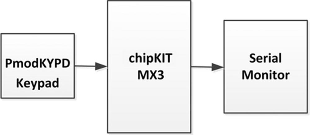
FIGURE 7.145 Block Diagram of the Project
7.28.3. Project Hardware
Figure 7.146 shows the hardware setup where the PmodKYPD module is connected to Pmod connector JA. The circuit diagram of the project is shown in Figure 7.147.
7.28.4. Project PDL
Before going into details of programming the keypad, it is worthwhile to look at the functions available for using the keypad.
The keypad library is available as a zip file at the Digilent web site under the PmodKYPD module specifications (document number DSD-0000337). Assuming that you have installed MPIDE in the default directory, the steps for loading the keypad library are given as follows:
• Copy the keypad library to a folder and unzip it. You should have the following files:
KYPD: C++ source file
KYPD: header file
keywords: text file
documents: folder (keypad documentation)
examples: folder (keypad example)
• Create a new folder with the name KYPD under the following subdirectory (assuming you have the same version of MPIDE) and copy all the unzipped files into this directory:
C:\MPIDE\mpide-0023-windows-20130715\hardware\pic32\libraries
• Start the MPIDE. Click Sketch → Import Library → KYPD.
You should see the header file KYPD.h copied to the beginning of your file.
After including the header file, we have to define the number of rows and columns on our keypad. For a 4 × 4 keypad, this can be done as follows:
const byte ROWS = 4;
const byte COLS = 4;
Then, we have to specify the structure of our keypad. For the 4 × 4 keypad that we will be using, this can be done as follows (notice that the characters on the keyboard matrix can be changed if desired):
We should now define the interface between the keypad and the chipKIT MX3 development board. In reference to Table 7.9, we can define the interface rows and columns as follows, starting from row 1 and column 1:
unsigned int RowPins[ROWS] = {7, 6, 5, 4};
unsigned int ColPins[COLS] = {3, 2, 1, 0};
Then, a keypad object should be created from the Keypad class as follows:
KYPD mykpd;
We can now use object mykpd with the various functions of the keypad library. A brief summary of the commonly used functions is given as follows:
mykpd.begin(): This function sets column pins for outputs and row pins for inputs.
mykpd.setPins(rows, cols): This function sets the pins for rows and columns.
mykpd.setKeyMap(keys): This function maps the key table.
mykpd.end(): This function releases the pins.
mykpd.getKey(): This function returns the key that is pressed (if any). The function is nonblocking. Returns −1 if no keys were pressed.
mykpd.getColRow(): This function returns 32-bit result. The column is returned in the most significant 16-bit, and the row in the least significant 16-bit. Returns −1 if no keys were pressed.
mykpd.getKey(colrow): In this function, colrow is the column–row indicator. The function returns the key pressed.
We can find the key pressed by either calling the getKey() function directly or calling the getColRow() function to find the column and row indicator and then use this value in the call getKey(colrow) to find the actual key pressed.
The project PDL is shown in Figure 7.148.
7.28.5. Project Program
The program is called KEYPAD1, and the program listing is given in Figure 7.149. At the beginning of the program, the keypad library KYPD.h is declared. Then, the structure and the interface of the keypad are defined in the setup() routine and also the Serial Monitor is initialised at 9600 Baud. Inside the main program loop, the program checks if a key is pressed and if so displays the pressed key on the Serial Monitor.
Figure 7.150 shows an example output from the program where the following keys were pressed on the keypad: 1237899FED.
7.29. Project 7.29 – Keypad Calculator
7.29.1. Project Description
In this project, we design a simple four-function (+, −, ×, /) calculator using the PmodKYPD keypad and the Serial Monitor.
The user first enters two numbers and then the operation to be performed. The result is calculated and displayed on the Serial Monitor.
In this project, the keypad is organised as follows:
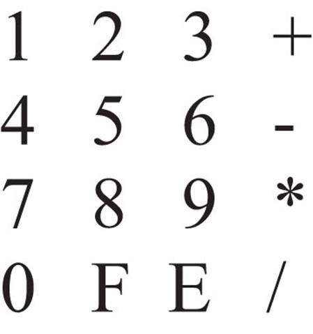
where E is the entry (return) key. The F key is not used. The operation of the calculator is shown as follows for multiplying two numbers as an example:
7.29.2. Project Hardware
The hardware setup and the circuit diagram are as in Figures 7.146 and 7.147, respectively.
7.29.3. Project PDL
The project PDL is shown in Figure 7.151.
7.29.4. Project Program
The program is called CALC, and its listing is shown in Figure 7.152. At the beginning of the program, the keypad library KYPD.h is included and various keypad keys are defined. The keypad map is stored in an array called keys. Inside the setup() routine, the Serial Monitor is initialised and the keypad library is mapped to the I/O ports.
Inside the main program loop, the first number, the second number, and the operation to be performed are read. The numbers are read using the following code:
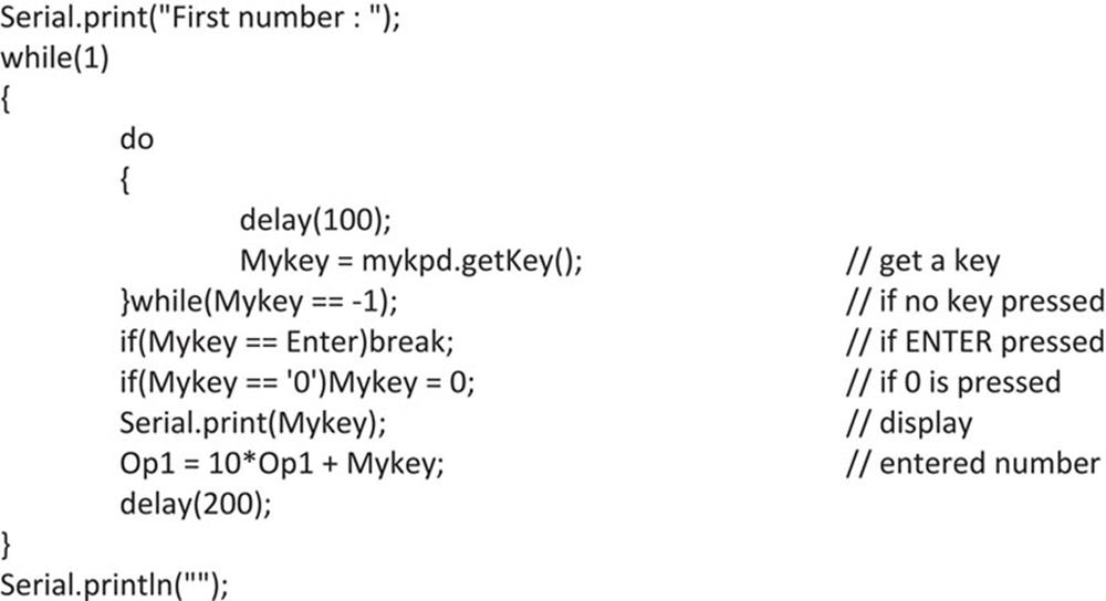
Keypad library routine mykpd.getKey() is used in a while loop until a key is pressed by the user. Notice that a small delay is used inside this loop to avoid multiple key presses. The program exits the while loop when the Enter key is pressed. Otherwise, the entered numbers are collected and the total number is stored in a variable called Op1 (or Op2 for the second number).
A switch loop is used to perform the required operation:
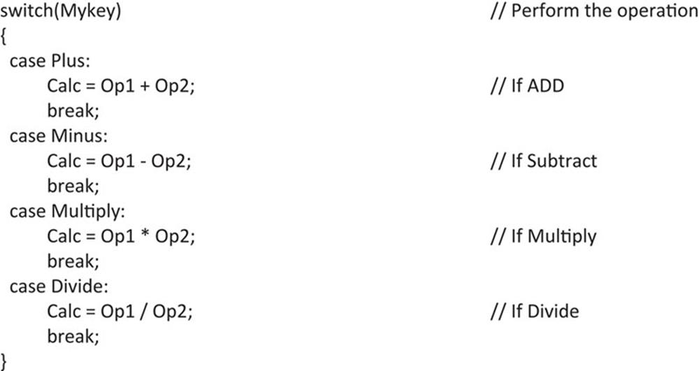
The result is in variable Calc and is displayed on the Serial Monitor.
A typical run of the program is shown in Figure 7.153.
7.30. Project 7.30 – Using Graphics LCD
7.30.1. Project Description
Graphics LCDs (GLCDs) are very useful in many embedded applications, requiring visual graphical outputs. There are many types of GLCDs such as monochrome, colour, TFT, organic (OLED), etc.
Two sizes of GLCDs are available as Pmod modules: the small-size PmodOLED and the bigger-size PmodOLED2. In this project, the smaller PmodOLED is used.
The PmodOLED is an organic 128 × 32 pixel GLCD having size 0.9 inches. The display uses the Solomon Systech SSD1306 display controller and is controlled from the standard SPI bus interface. The display module is model UG2832, and it operates at clock rates up to 10 MHz and is connected to the chipKIT MX3 development board through a 12-pin connector.
Figure 7.154 shows a picture of the PmodOLED module.
The origin of the display is the top left-hand corner with the X-axis running horizontal from 0 to 127. Similarly, the vertical axis is the Y-axis and runs from 0 to 31. Figure 7.155 shows the display coordinates.
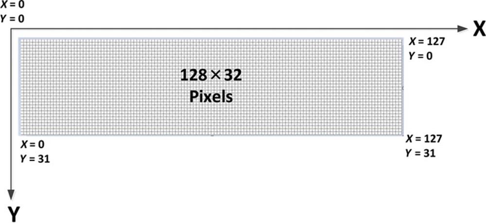
FIGURE 7.155 Display Coordinates
In this project, various shapes are drawn on the PmodOLED module in order to illustrate the principles of using the display.
The block diagram of the project is shown in Figure 7.156.
7.30.2. Project Hardware
The PmodOLED display is connected to Pmod connector JE where the SPI bus is located. The pin configuration of the display is shown in Table 7.10. Figure 7.157 shows the hardware setup. The circuit diagram of the project is shown in Figure 7.158.
Table 7.10
PmodOLED pin configuration
|
Connector J1 |
||
|
Pin |
Signal |
Description |
|
1 |
CS |
SPI chip select (slave select) |
|
2 |
SDIN |
SPI data in (MOSI) |
|
3 |
None |
Unused pin |
|
4 |
SCLK |
SPI clock |
|
7 |
D/C |
Data/command control |
|
8 |
RES |
Power reset |
|
9 |
VBATC |
VBAT battery voltage control |
|
10 |
VDDC |
VDD logic voltage control |
|
5, 11 |
GND |
Power supply ground |
|
6, 12 |
VCC |
Power supply |
The PmodOLED module has two power supplies: VDD is the power to the display logic, and Vbat is the power to the actual display. The display/control (D/C) pin determines whether the bytes sent to the display should be interpreted as data or commands. The RES pin when driven LOW resets the display, and must be set HIGH for normal operation. The CS, SDIN, and SCLK are the standard SPI bus interface signals.
7.30.3. Project PDL
The PmodOLED library provides a large number of functions for using the display. This library is available in the Digilent PmodOLED product page (DSD-0000319) and should be installed into the MPIDE environment before it can be used. Assuming that you have installed MPIDE in the default directory, the steps for loading the OLED library are given as follows:
• Copy the OLED library to a folder and unzip it. You should have the following files:
OLED: C++ source file
OLED: header file
keywords: text file
documents: folder (keypad documentation)
examples: folder (keypad example)
Some other files
• Create a new folder with the name OLED under the following subdirectory (assuming you have the same version of MPIDE) and copy all the unzipped files into this directory:
C:\MPIDE\mpide-0023-windows-20130715\hardware\pic32\libraries
• Start the MPIDE. Click Sketch → Import Library → OLED.
The following header files must be included at the beginning of your file:
#include <OLED.h>
#include <DSPI.h>
The display memory is organised such that the first byte (byte 0) corresponds to a vertical column of eight pixels at the left side of the display, with the least significant bit the uppermost pixel in the column. The next byte corresponds to the next column of eight pixels to the right of the first. This continues across the display to byte 127, which is the rightmost column of eight pixels. Byte 128 corresponds to the next column of eight pixels at the left of the display.
The display can operate in graphics or in character mode. The character can be selected. With the standard character size = 1, the character set is 5 × 7 dot matrix. With one pixel margin at the right and one pixel margin at the bottom, the character size is 6 × 8 pixels. The selected size value multiplies the height and width by the size. For example, with size = 2, the character will be (2 × 6) × (2 × 8) = 12 × 16 pixels. With 128 × 32 pixels and size = 1, there can be up to 4 lines of text and each line can have 128 /6 = 21 characters across, that is, the character display size is 4 rows × 21 columns (the character coordinates are 0 based, that is, 0–3 rows and 0–20 columns). With size = 2, there can be up to 2 lines of text and each line can have 128/12 = 10 characters across, that is, the character display size is 2 rows × 10 columns (0–1 row and 0–9 columns).
A brief summary of the commonly used OLED functions is given below.
General functions
OLED.begin(): This function initialises the display and turns power to the display. It must be called before calling any other OLED function.
OLED.end(): This function turns power off to the display and frees the SPI pins used for the display.
OLED.displayON():This function activates the display.
OLED.displayOFF():This function blanks the display.
OLED.clear():This function clears the memory buffer and hence the display.
Character functions
OLED.setCursor(horz, vert): This function sets the horizontal (x) and vertical (y) character positions to the specified location.
OLED.getCursor(horz, vert): This function returns the horizontal (x) and vertical (y) character positions.
OLED.setCharUpdate(f): This function enables (nonzero) or disables (zero) automatic character update.
OLED.putchar(c): This function writes the specified character at the current cursor position and advances the cursor.
OLED.putString(str): This function writes the specified NULL terminated string to the display and advances the cursor.
Graphics functions
OLED.setDrawColor(clr): This function sets the foreground colour used for pixel draw.
OLED.getstdPattern(pat): This function returns a pointer for the specified pattern number.
OLED.setFillPattern(pat): This function sets a pointer to a fill pattern. There are eight fill patterns to choose from.
OLED.moveTo(x, y): This function sets the current graphics drawing coordinate to x, y.
OLED.getPos(x, y): This function returns the current graphics drawing coordinate.
OLED.drawPixel(): This function sets the pixel at the current drawing position.
OLED.drawLine(x, y): This function draws a line from the current pixel position to the specified position. Cursor is set at the new position.
OLED.drawRect(x, y): This function draws a rectangle bounded with the current location and the specified corners.
OLED.drawFillRect(x, y): This function fills a rectangle without drawing an outline around the rectangle.
OLED.putBmp(x, y, bmp): This function draws the specified bitmap.
OLED.drawChar(c): This function draws the specified character at the current location.
OLED.drawstring(str): This function writes the specified NULL terminated string to the display.
The PDL of the program is shown in Figure 7.159. The program displays the following strings and shapes:
“chipKIT”
“MX3”
“Development”
“Kit”
Rectangle at centre of display
Rectangle at centre of display with eight different fill patterns
X–Y-axis at the centre of display
X–Y-axis at bottom left of the display
7.30.4. Project Program
The program is named OLED1, and its listing is given in Figure 7.160. At the beginning of the program, the SPI library and the OLED library are included in the program. In the setup() routine, the OLED is initialised and power applied to the module. Inside the main program loop, the character cursor is positioned to the left-hand side of the display and the following text is displayed:
Row 1: “chipKIT”
Row 2: “MX3”
Row 3: “Development”
Row 4: “Kit”
The program then waits for 5 s and blinks the display ON and OFF three times with 1-s delay between each blinking. After 5-s delay, the program displays a rectangle at the centre of the display. The graphics cursor is first set at coordinate (55, 1), which is the top left corner of the rectangle. The bottom right-hand corner of the rectangle is then set to (75, 27). The rectangle is displayed for 5 s. The program then establishes a for loop that executes eight times. Inside this loop, a rectangle is drawn and is filled with a different pattern at each iteration (pattern 0 is with no filling). Each pattern is displayed for 2 s. After 5-s delay, the program draws an X–Y-axis where the origin is at the centre of the display. Finally, another X–Y-axis is drawn with the centre at the bottom left corner of the display.
Figures 7.161–7.165 show the outputs on the display.
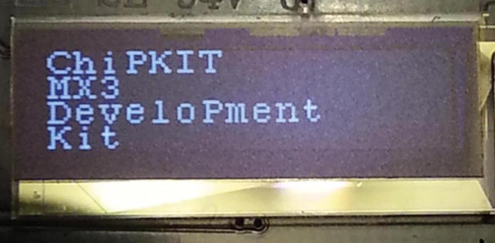
FIGURE 7.161 Displaying the Text
FIGURE 7.162 Displaying a Rectangle
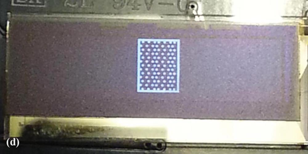
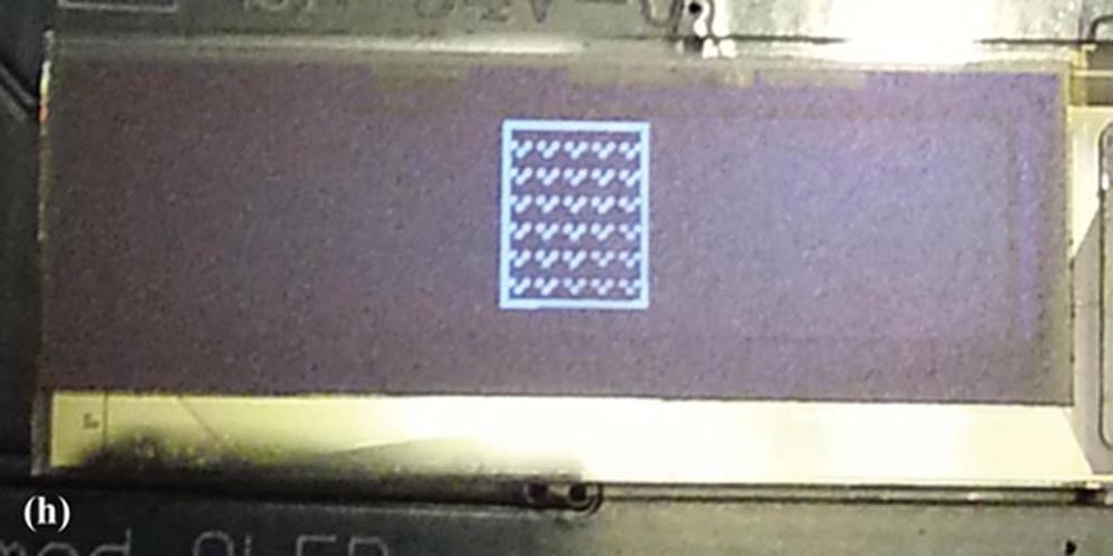
FIGURE 7.163 (a) Rectangle With Pattern 0. (b) Rectangle With Pattern 1. (c) Rectangle With Pattern 2. (d) Rectangle With Pattern 3. (e) Rectangle With Pattern 4. (f) Rectangle With Pattern 5. (g) Rectangle With Pattern 6. (h) Rectangle With Pattern 7.
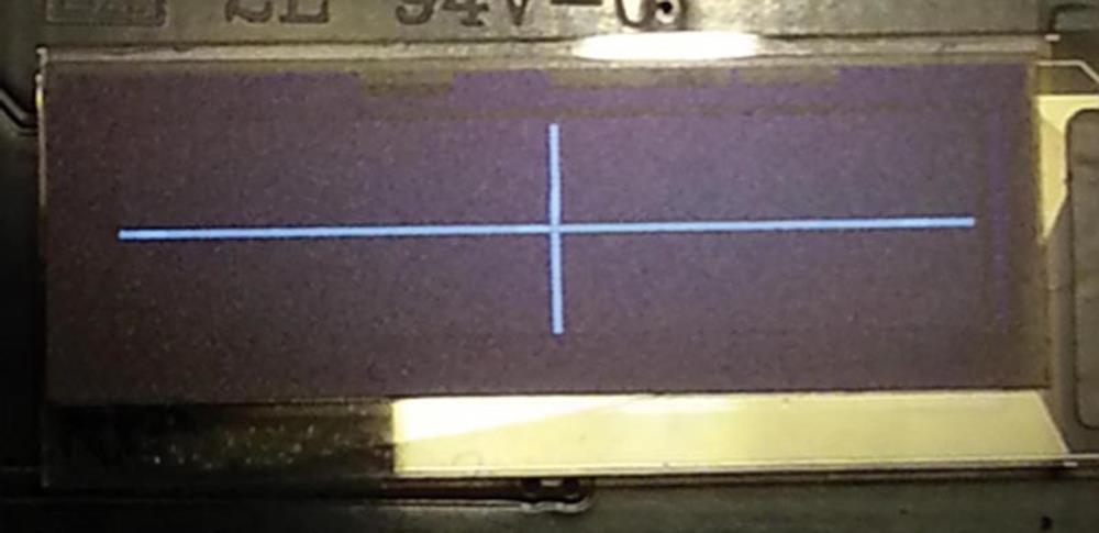
FIGURE 7.164 X–Y-Axis at the Centre of the Display
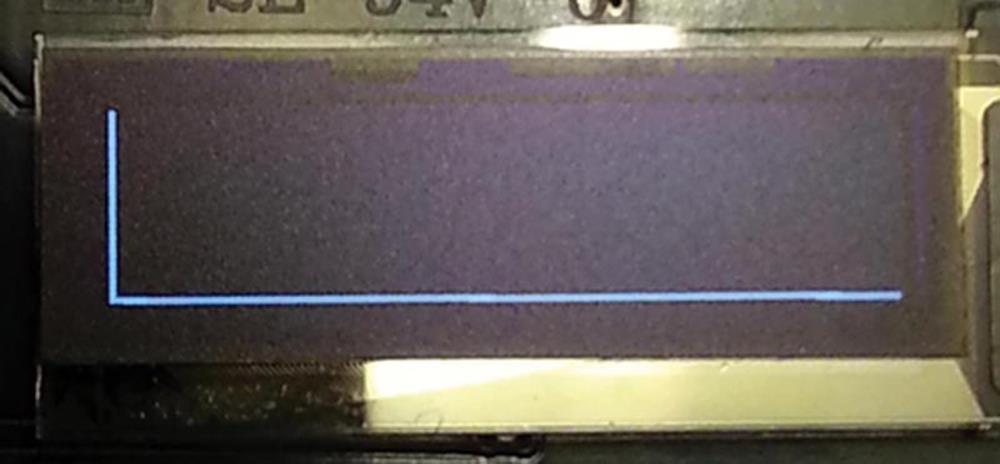
FIGURE 7.165 X–Y-Axis at the Bottom Left Corner of the Display
7.31. Project 7.31 – Creating an Image on the OLED
7.31.1. Project Description
In some applications, we may want to create and display our own images (e.g., a logo) on the OLED. In this section, the steps are given for creating and displaying a simple image.
The block diagram, hardware setup, and the circuit diagram of the project are as in Figures 7.156–7.158, respectively. PmodOLED is connected to Pmod connector JE as in the previous project.
Creating the image
The image must be in bitmap (.bmp) format with the pixel size 128 × 32. There are many programs that can be helpful for creating bitmap images. Perhaps the easiest one is the Paint program, which is distributed free of charge with the Windows operating system. The steps for creating an image are given as follows:
• Start the Paint program (usually in folder Accessories).
• Click left-hand menu and select Properties.
• Set the width to 128 and height to 32 pixels (see Figure 7.166).
• Click Zoom in icon until the size of the bitmap is big enough.
• Draw your image using the cursor. In this example, the image consists of four rectangles as shown in Figure 7.167.
FIGURE 7.167 The Image Used in This Example
• Save the image as a BMP picture by clicking the Save As button and giving a name to the image.
• Now, the image should be converted to an array of bitmap values. There are several programs that can be used for this purpose. The one used in this project is called LCD Assistant and is available at the web site: http://en.radzio.dxp.pl/bitmap_converter.
• Start the LCD Assistant program. Click File → Load image and load your bitmap image created earlier. Select (see Figure 7.168):
Byte orientation = vertical
Width = 128, height = 32
Size endianness = little
Pixels/byte = 8
and give a name to your output file (in this example, the name BOXES is given).
• Click File → Save output and save the file in a folder.
• Start the MPIDE development environment, including the SPI and the OLED libraries. Additionally, include the bitmap array file created above.
The program listing (OLED2) for this project is shown in Figure 7.169. The bitmap image is displayed by calling OLED function OLED.putBmp with the size of the image and the bitmap array filename. In this example, the bitmap array file was stored in folder C:\.
Figure 7.170 shows the created image being displayed.
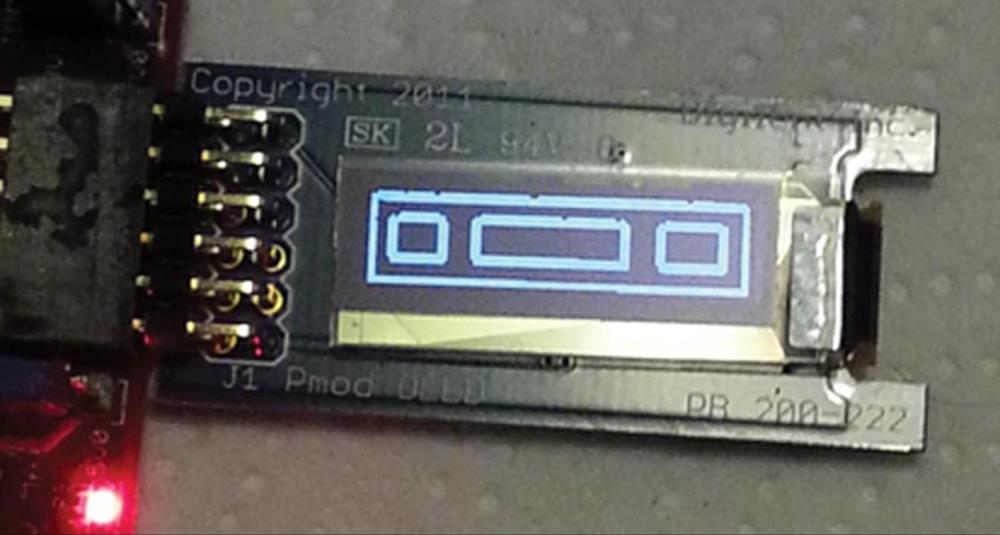
FIGURE 7.170 The Created Image
7.32. Project 7.32 – I2C Thermometer With OLED Display
7.32.1. Project Description
In this project, we will be using the PmodTMP2 I2C-based temperature sensor module to measure the ambient temperature and display it on the PmodOLED module in graphical form.
PmodTMP2 is a high-accuracy digital temperature sensor module using the ADT7420 (Analog Devices) temperature sensor chip. The module is based on the I2C bus interface and acts as a slave device. The basic features of the ADT7420 chip are:
• Temperature accuracy of ±0.20°C from −10 to +85°C at 3.0 V
• Temperature accuracy of ±0.25°C from −20 to +105°C from 2.7 to 3.3 V
• Fast temperature conversion (240 ms continuous)
• Low-power operation (700 μW at 3.3 V operation)
• Overtemperature and undertemperature control pins
The module has 2 × 4 pins for connecting to the Pmod connectors. The module has four selectable addresses.
Figure 7.171 shows a picture of the PmodTMP2 module. The interface connector (J1) pin layout is shown in Table 7.11. The I2C interface uses the two signals SCL and SDA. Module address is selected using two jumpers (JP1 and JP2) as shown in Table 7.12. By default, the jumpers are not connected and the default module address is 0x4B.
Table 7.11
PmodTMP2 interface connector.
|
Connector J1 – I2C Communications |
||
|
Pin |
Signal |
Description |
|
1, 2 |
SCL |
I2C clock |
|
3, 4 |
SDA |
I2C data |
|
5, 6 |
GND |
Power supply ground |
|
7, 8 |
VCC |
Power supply (3.3 V/5 V) |
Table 7.12
PmodTMP2 module address selection.
|
JP2 |
JP1 |
Address |
|
Open |
Open |
0×4B (0b1001011) |
|
Open |
Shorted |
0×4A (0b1001010) |
|
Shorted |
Open |
0×49 (0b1001001) |
|
Shorted |
Shorted |
0×48 (0b1001000) |
The module provides two open drain outputs for controlling external devices in temperature threshold applications. The module is configured such that when powered up it can be used as a simple temperature sensor without any configuration. At start-up, a 2-byte read without specifying a register will read the value of the temperature from the device, where the first byte will be the most significant byte and the second byte is the least significant byte in the form of 2’s complement notation. If the result is shifted right by 3 bits (this is because the 3 least significant bits of the returned data are the event alarm flags for overtemperature and undertemperature conditions) and multiplied by 0.0625 (this is because each LSB of the returned value corresponds to 0.0625°C), then the resulting signed floating point value will be the temperature reading in degrees centigrade.
The block diagram of the project is shown in Figure 7.172.
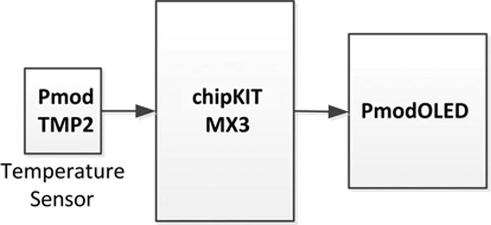
FIGURE 7.172 Block Diagram of the Project
7.32.2. The I2C Bus
Before going into the details of the project hardware, it is worthwhile to review the basic principles of the I2C bus communications protocol. I2C is a bidirectional two-line communication between a master and one or more slave devices. The two lines are named SDA (serial data) and SCL (serial clock). Both lines must be pulled up to the supply voltage using suitable resistors. Figure 7.173 shows a typical system configuration with one master and three slaves communicating over the I2C bus.
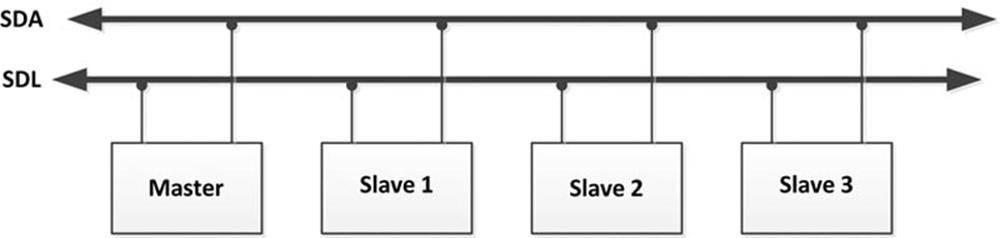
FIGURE 7.173 I2C System Configuration
Most high-level language compilers provide libraries for I2C communication. We can also easily develop our own I2C library. Although the available libraries can easily be used, it is worthwhile to look at the basic operating principles of the bus.
The I2C bus must not be busy before data can be sent over the bus. Data is sent serially, and synchronised with the clock. Both SDA and SCL lines are HIGH when the bus is not busy. The START bit is identified by the HIGH-to-LOW transition of the SDA line while the SCL is HIGH. Similarly, a LOW-to-HIGH transition of the SDA line while the SCL is HIGH is identified as the STOP bit. Figure 7.174 shows both the START and STOP bit conditions.
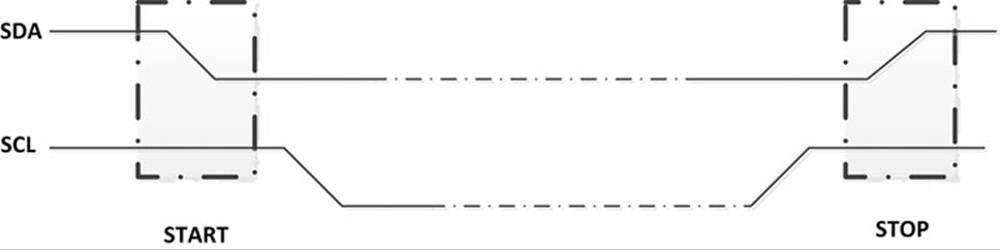
FIGURE 7.174 START and STOP Bit Conditions
1 bit of data is transferred during each clock pulse. Data on the bus must be stable when SCL is HIGH; otherwise, the data will be interpreted as a control signal. Data can change when the SCL line is LOW. Figure 7.175 shows how bit transfer takes place on the bus.
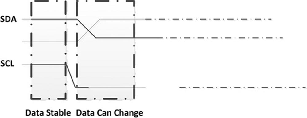
FIGURE 7.175 Bit Transfer on the Bus
Each byte of 8 bits on the bus is followed by an acknowledgement cycle. The acknowledgement cycle has the following requirements:
• An addressed slave device must generate an acknowledgement after the reception of each byte from the master.
• A master receiver must acknowledge after the reception of each data byte from the slave (except the last byte).
• The acknowledge signal is identified by a device by lowering the SDA line during the acknowledge clock HIGH pulse.
• A master receiver must signal the end of data to the transmitter by not lowering the SDA line during the acknowledge clock HIGH pulse. In this case, the transmitter leaves the SCL line HIGH so that the master can generate the STOP bit.
The communication over the I2C bus is based on addressing where each device has a unique 8-bit address, usually set up by hardware configuration. Before sending any data, the address of the device that is expected to respond is sent after the START bit.
7.32.3. Project Hardware
Header J2 on the chipKIT MX3 provides the I2C signal interface, and the PmodTMP2 must be connected to this header (see Figure 7.176a and b) through the cable and connector assembly supplied with the PmodTMP2 module.
Since the PmodTMP2 has open collector outputs, the pull-up resistors on the board must be enabled. Shorting blocks must be installed in jumpers JP1 and JP10 near the Pmod connector JA in order to enable the pull-up resistors. Figure 7.177 shows the hardware setup of the project. The circuit diagram of the project is shown in Figure 7.178.
The chipKIT I2C library called WIRE is used to access the I2C signals. This library is normally included in the MPIDE development environment.
The file Wire.h must be included at the beginning of your programs in order to use the I2C interface. The following functions are offered by this library:
Wire.begin(): This function initialises the I2C library and must be called before calling other functions. Optionally the 7-bit slave device address can be specified; otherwise, the interface is a master.
Wire.write(data) or Wire.write(string) or Wire.write(data, length): This function sends data over the bus.
Wire.read(): This function reads a byte from the bus.
Wire.beginTransmission(address): This function starts transmission with a slave device whose address is given.
Wire.endTransmission(): This function ends transmission to a slave device that was begun.
Wire.requestFrom(address, quantity): This function is used by the master to request bytes from a slave device. The bytes may then be retrieved with the available() and read() functions. The 7-bit address of the device to request bytes from and the number of bytes requested are arguments of the function.
Wire.available(): This function returns the number of bytes available for retrieval with the read() function.
Wire.onReceive(handler): This function registers a function to be called when a slave device receives a transmission from a master.
Wire.onRequest(handler): This function registers a function to be called when a master requests data from a slave device.
Figure 7.179 shows the PDL of the project.
7.32.5. Project Program
The program is named I2C, and the program listing is shown in Figure 7.180. Although the PmodTMP2 module can measure both negative and positive temperatures, only positive temperatures are displayed in this project. At the beginning of the program, the I2C, SPI, and OLED libraries are included in the program and various variables used in the program are created. Inside the setup() routine, the OLED is initialised and powered ON, I2C interface signals are initialised, and X–Y-axis is drawn on the OLED with its origin at the bottom left corner of the display. Inside the main program loop, the MSB and LSB bytes of the temperature are read from the PmodTMP2 module by calling the I2C functions requestFrom and receive. The address of the PmodTMP2 module and the number of bytes requested from the slave device are specified as 0x4B and 2, respectively. Then, the temperature is calculated in degrees centigrade by shifting right 3 bits and multiplying with 0.0625. The temperature is converted into a string and displayed starting from character position (10, 2) of the display. The Y pixel value of the temperature is calculated by subtracting the integer value of the temperature from 31. Thus, for example, if the temperature is 10°C, then this will be shown as a pixel at display coordinate Y = 21, and so on. Therefore, the display can show temperature values from 0°C (at the bottom of the display, corresponding to actual display coordinate Y = 31) to up to 31°C (at the top of the display, corresponding to actual display coordinate Y = 0). The time is incremented in steps of 10 s, that is, each horizontal pixel corresponds to 10 s. When the end of the horizontal axis is reached, the X value is cleared, axes are redrawn, and the display continues from the beginning. Notice that during the first iteration, the X value is set to 0 so that display starts from the left-hand side and also the axes are drawn.
A typical output on the display is shown in Figure 7.181.
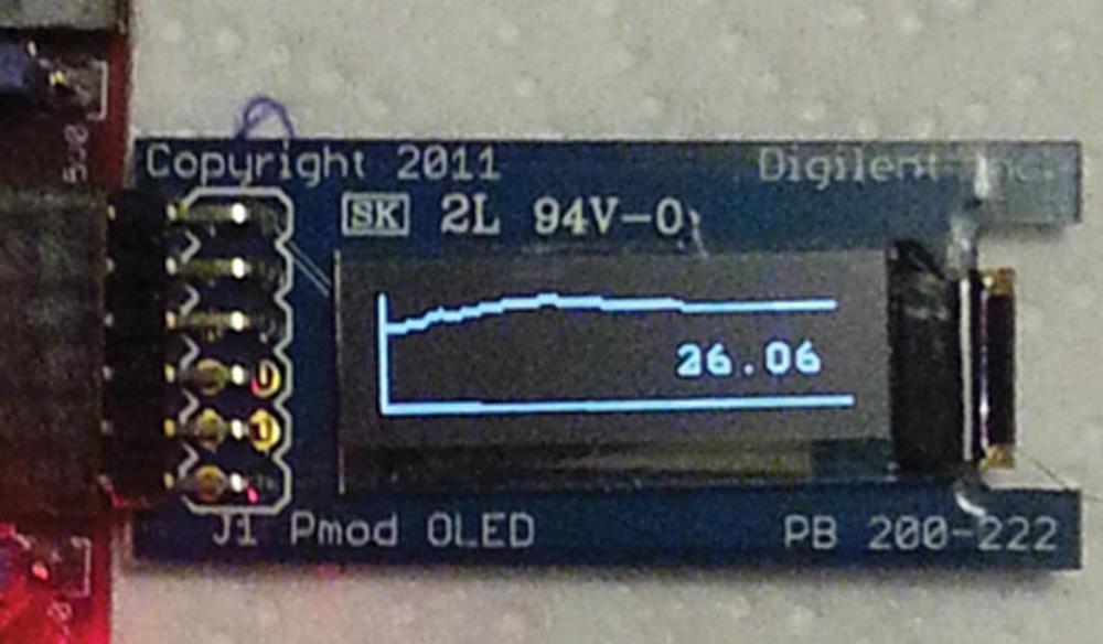
FIGURE 7.181 Typical Output on the Display
7.33. Project 7.33 – Using the GPS Module
7.33.1. Project Description
In this project, we will be using the PmodGPS module to get the navigational parameters of our current location on Earth and then to display them on the Serial Monitor.
The GPS is a satellite-based system that provides location (latitude, longitude, altitude) and time information anywhere on Earth and at any time and in all weather conditions. The system was originally developed for military use but is now freely available to anyone with a GPS receiver.
The GPS system was developed in 1973 by the U.S. Department of Defense, and originally it had 24 satellites orbiting the Earth. The satellites are positioned such that at any time a minimum of four satellites are visible from anywhere on Earth. The determination of the latitude and longitude requires information from at least three satellites. The altitude requires a fourth satellite to be available. In practise, up to 10 satellites can be in view in open space.
The GPS system consists of three major segments: space segment, control segment, and user segment. The U.S. Air Force develops, maintains, and operates the space and control segments. Currently the space segment consists of 24–32 satellites in orbit around the Earth. The control segment consists of a master control station and alternate control stations. The user segment consists of the user GPS receivers.
A GPS receiver is a small handheld battery-operated device the size of a mobile phone. It receives signals from the visible satellites and determines the owner’s location on Earth with high precision (around 3 m). In general, GPS receivers are composed of an antenna, a processor, and usually a graphical display to show user’s navigational parameters. A receiver is often described by its number of channels: this signifies how many satellites it can monitor simultaneously. Currently most low-cost receivers have at least 12 channels.
GPS receivers may additionally include an external input for differential corrections, using the RTCM SC-104 data format. This correction is in the form of an RS-232 serial data at 4800 bits/s. Some receivers have internal correction channels known as Wide Area Augmentation System (WAAS). With this channel, the overall accuracy and integrity of a receiver are enhanced.
Most GPS receivers can send out position data to a PC or any other suitable device using the NMEA 0183 protocol. This protocol basically consists of sentences starting with identifier character “$,” followed by a word that identifies the sentence type, and then the navigational data are given, separated with commas. Different GPS receivers send out different types of NMEA 0183 sentences.
In this project, we will be receiving the NMEA 0183 sentences from a PmodGPS module and then display them on the Serial Monitor.
Figure 7.182 shows a picture of the PmodGPS module.
The basic features of the PmodGPS module are:
• Six-pin Pmod connector
• Operating voltage 3–3.6 V
• Low power consumption (24–30 mA)
• Built-in antenna (external antenna capability on header J4)
• Horizontal accuracy of 3 m
• Operation with two-wire UART interface
• RTCM SC-104–compatible differential correction capability
• Optional 3 V coin cell battery to reduce the amount of time it takes to acquire the first positional fix
The PmodGPS module operates with serial communication at 9600 Baud (can be increased if required), 8 data bits, no parity bit, and 1 stop bit. The first time the device is powered, it can take up to 2 min to display the positional data. After the first time, acquisition time is reduced to less than 30 s.
Figure 7.183 shows the block diagram of the project.
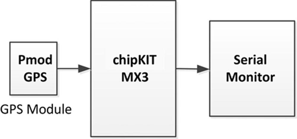
FIGURE 7.183 Block Diagram of the Project
7.33.2. Project Hardware
The PmodGPS is interfaced with the chipKIT MX3 development board through its J1 connector. Table 7.13 shows the J1 pin layout of this connector. The 3DF pin (pin 1) indicates the status of the positional fix, and it stays LOW when a fix is obtained. This pin is toggled every second if a fix cannot be obtained. Also, the green light (LD1) on the board flashes every second if a fix is not obtained. This light turns OFF when a fix is obtained.
Table 7.13
PmodGPS connector J1 pin layout.
|
Pin |
Signal |
Description |
|
1 |
3DF |
3D-Fix indicator |
|
2 |
RX |
Receive |
|
3 |
TX |
Transmit |
|
4 |
1PPS |
1 pulse per second |
|
5 |
GND |
Power supply ground |
|
6 |
VCC |
Power supply (3.3 V/5 V) |
Pins 2 and 3 are the serial communication receive and transmit pins, respectively. Pin 4 is the one pulse per second pin (not used in this project). The two-pin connector J2 consists of the Reset and differential correction pins and is not used in this project.
chipKIT MX3 UART interface
The PIC32MX320 microcontroller provides two UART interfaces (UART1 and UART2) with two- or four-wire asynchronous serial interfaces. In this project, the two-wire interface is used with the receive (RX) and transmit (TX) pins. In this project, UART2 interface is used (notice that the Serial Monitor software uses UART1 and using this port for the GPS may interfere with operation of the Serial Monitor).
This interface is accessed from Pmod connector JC (UART1 interface is accessed from JB). The pin configuration of UART2 is:
• JC-01 (logical I/O port 16), UART1 CTS (Clear to Send) pin
• JC-02 (logical I/O port 17), UART1 TX pin
• JC-03 (logical I/O port 18), UART1 RX pin
• JC-04 (logical I/O port 19), UART1 RTS (Request to Send) pin
The hardware setup is shown in Figure 7.184 where the PmodGPS module is connected to the upper row of Pmod connector JC. Figure 7.185 shows the circuit diagram of the project.
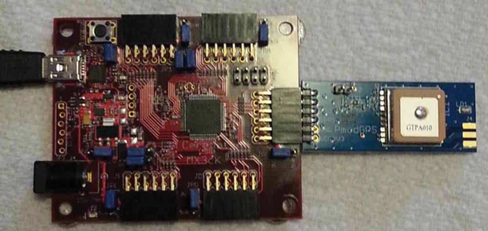
FIGURE 7.184 Hardware Setup
When using the chipKIT MX3 development board with MPIDE development environment, the chipKIT serial communications library SoftwareSerial can be used.
7.33.3. Project PDL
The chipKIT SoftwareSerial library provides serial communications capability through any required I/O port of the microcontroller. Because this library is implemented in software, it has the following limitations:
• Only speeds up to 9600 Baud are supported.
• There is no function to check if data is available at the receive buffer.
• The read function is blocking and waits until data becomes available.
• Data received when the receive function is not called is lost, that is, the received data is not stored in a buffer for future use.
The following functions are provided with the SoftwareSerial library:
SoftwareSerial(RXpin, TXpin): This function creates a serial object where the receive (Rxpin) and transmit (Txpin) pins must be specified as arguments to the function.
begin(Baud): This function sets the communications Baud rate.
read(): This function waits for a character to be available at the serial port and then reads it.
print(data): This function writes a character (data) to the serial port.
println(data): Similar to print() but a new line is sent to the serial port at the end of the data.
The project PDL is shown in Figure 7.186.
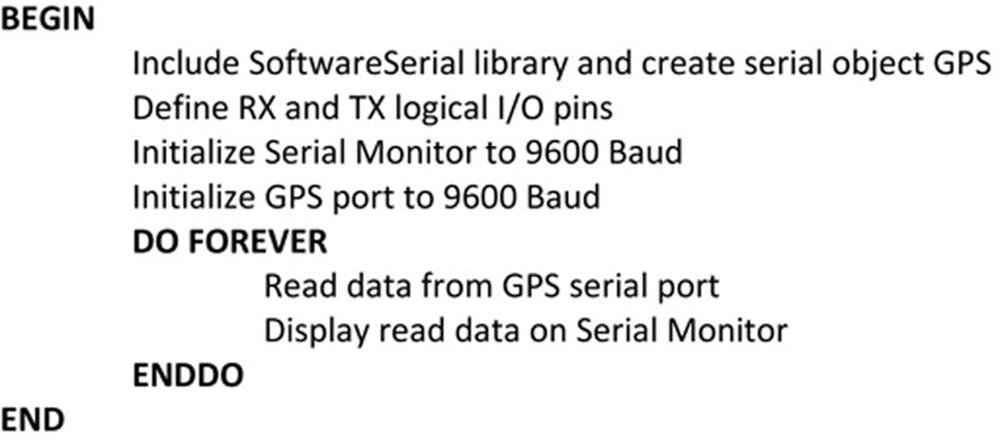
FIGURE 7.186 Project PDL
7.33.4. Project Program
The program is named GPS, and its listing is shown in Figure 7.187. At the beginning of the program, SoftwareSerial library is included and the logical I/O port numbers of the receiver and transmit pins are defined. The serial object is named GPS. Inside the setup()routine, the Serial Monitor and the GPS serial port are initialised to operate at 9600 Baud.
The operation of the main program loop is very simple. Here, function GPS.read reads a byte from the PmodGPS module. This byte is then sent to the Serial Monitor by calling function Serial.write.
Figure 7.188 shows the data received from the PmodGPS module every second. The decoding of some of the sentences is given in Figures 7.189 and 7.190 (further information can be obtained from the PmodGPS product data sheet).
7.34. Project 7.34 – Stepper Motors
7.34.1. Project Description
This project is about using stepper motors in microcontroller-based systems. This is an introductory project where a stepper motor is driven from a microcontroller.
Before going into the details of the project, it is worthwhile to look at the theory and operation of stepper motors briefly.
Stepper motors are commonly used in printers, disk drives, position control systems, and many more systems where precise position control is required. Stepper motors come in a variety of sizes, shapes, strengths, and precision. There are two basic types of stepper motors: unipolar and bipolar.
Unipolar stepper motors
Unipolar stepper motors have two identical and independent coils with centre taps, and have five, six, or eight wires (see Figure 7.191).
FIGURE 7.191 Unipolar Stepper Motor Windings
Unipolar stepper motors can be driven in three modes: one-phase full-step sequencing, two-phase full-step sequencing, and two-phase half-step sequencing.
One-phase full-step sequencing
Table 7.14 shows the sequence of sending pulses to the motor. Each cycle consists of four pulses.
Table 7.14
One-phase full-step sequencing.
|
Step |
a |
c |
b |
d |
|
1 |
1 |
0 |
0 |
0 |
|
2 |
0 |
1 |
0 |
0 |
|
3 |
0 |
0 |
1 |
0 |
|
4 |
0 |
0 |
0 |
1 |
Two-phase full-step sequencing
Table 7.15 shows the sequence of sending pulses to the motor. The torque produced is higher in this mode of operation.
Table 7.15
Two-phase full-step sequencing.
|
Step |
a |
c |
b |
d |
|
1 |
1 |
0 |
0 |
1 |
|
2 |
1 |
1 |
0 |
0 |
|
3 |
0 |
1 |
1 |
0 |
|
4 |
0 |
0 |
1 |
1 |
Two-phase half-step sequencing
Table 7.16 shows the sequence of sending pulses to the motor. This mode of operation gives more accurate control of the motor rotation, but requires twice as many pulses for each cycle.
Table 7.16
Two-phase half-step sequencing.
|
Step |
a |
c |
b |
d |
|
1 |
1 |
0 |
0 |
0 |
|
2 |
1 |
1 |
0 |
0 |
|
3 |
0 |
1 |
0 |
0 |
|
4 |
0 |
1 |
1 |
0 |
|
5 |
0 |
0 |
1 |
0 |
|
6 |
0 |
0 |
1 |
1 |
|
7 |
0 |
0 |
0 |
1 |
|
8 |
1 |
0 |
0 |
1 |
The motor can be connected to a microcontroller using power transistors or power MOSFET transistors.
Bipolar stepper motors
Bipolar stepper motors have two identical and independent coils and four wires, as shown in Figure 7.192.
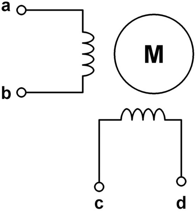
FIGURE 7.192 Bipolar Stepper Motor Windings
The control of bipolar stepper motors is slightly more complex. Table 7.17 shows the typical driving sequence. The “1” and “0” denote the logic levels applied to the motor legs. Bipolar stepper motors are usually driven using H-bridge circuits.
Table 7.17
Bipolar stepper motor driving sequence.
|
Step |
a |
c |
b |
d |
|
1 |
1 |
1 |
0 |
0 |
|
2 |
0 |
1 |
1 |
0 |
|
3 |
0 |
0 |
1 |
1 |
|
4 |
1 |
0 |
0 |
1 |
The bipolar consists of two coils, but there is no centre tap. As a result of this, the bipolar motor requires a controller where the current flow through the coils can be reversed. A bipolar motor is capable of higher torque since entire coils may be energised, not just half of the coils. Bipolar stepper motors are usually controlled using H-bridge circuits where the current flow through the coils can easily be reversed.
In this project, a bipolar stepper motor is used. The motor is rotated 10 revolutions in one direction, then stopped for 5 s, and then rotated 10 revolutions in the other direction, and is then stopped. The PmodSTEP stepper motor controller module is used in this project.
Figure 7.193 shows the block diagram of the project.
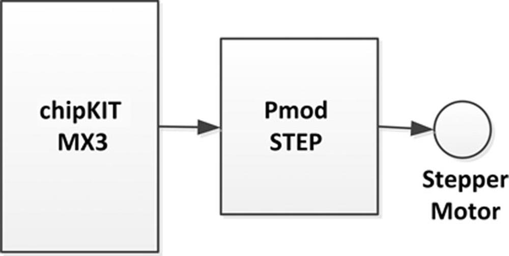
FIGURE 7.193 Block Diagram of the Project
7.34.2. Project Hardware
Figure 7.194 shows a picture of the PmodSTEP stepper motor controller module. This module is based on the L293D, which is a quadruple half-H motor controller chip. The PmodSTEP has the following features:
• External power for larger motors
• Signal status and power LEDs
• Compatibility with Pmod connectors
The L293D motor controller chip has the following features:
• 4.5–36 V supply voltage
• Up to 600 mA current per channel (peak 1.2 A)
• Output clamp diodes for transient suppression
• TTL-compatible logic inputs
• Easy control via Enable inputs
The L293D chip contains four high-current driver inputs named 1A–4A, with corresponding outputs named as 1Y–4Y. As shown in the logic diagram in Figure 7.195, 1A and 1B drivers are enabled using the 1,2EN pins. Similarly, 3A and 4A drivers are enabled using the 3,4EN logic pins.
PmodSTEP module is connected to the development board through Pmod connector J1. This connector has connections to the L293D chip with the following pin configuration:
|
Pin Number |
Function |
|
1 |
SIG1 |
|
2 |
SIG2 |
|
3 |
SIG3 |
|
4 |
SIG4 |
|
5 |
GND |
|
6 |
VCC |
|
7 |
SIG5 (input 1A) |
|
8 |
SIG6 (input 2A) |
|
9 |
SIG7 (input 3A) |
|
10 |
SIG8 (input 4A) |
|
11 |
GND |
|
12 |
VCC |
All the J1 signals (SIG1–SIG8) drive LEDs through MOSFET switching transistors so that the state of each pin can be observed. The outputs of the L293D chip are brought to a four-pin header called J2 with the following pin configuration:
|
Pin Number |
Function |
|
1 |
SM1 (output 1Y) |
|
2 |
SM2 (output 2Y) |
|
3 |
SM3 (output 3Y) |
|
4 |
SM4 (output 4Y) |
External power to the PmodSTEP module can be selected via the JP1 jumper. In this project, the internal +5 V is used to provide power to the motor and also to the controller module.
The PmodSTEP module is connected to Pmod connector JA, and the JA power jumper is set to +5 V so that +5 V power is applied to the module. PmodSTEP jumper JP1 is set to VCC (left position) so that power is taken from the VCC and not from an external source.
The interface between the PmodSTEP module and the development board is thus as follows:
|
JA Pin Number |
Logical I/O Port Number |
Port |
PmodSTEP Pin |
|
JA-01 |
0 |
RE0 |
SIG1 (not used) |
|
JA-02 |
1 |
RE1 |
SIG2 (not used) |
|
JA-03 |
2 |
RE2 |
SIG3 (not used) |
|
JA-04 |
3 |
RE3 |
SIG4 (not used) |
|
JA-07 |
4 |
RE4 |
SIG5 (input 1A) |
|
JA-08 |
5 |
RE5 |
SIG6 (input 2A) |
|
JA-09 |
6 |
RE6 |
SIG7 (input 3A) |
|
JA-10 |
7 |
RE7 |
SIG8 (input 4A) |
The type of motor used in this project is the 39HS02 (see Figure 7.196). This motor has the following features:
• Bipolar stepper motor
• 1.8° step angle (200 steps for a complete revolution)
• ±5% step angle accuracy
• 0.6 A phase current
• Four leads (coil 1: brown + grey, coil 2: orange + green)
Figure 7.197 shows the hardware setup of the project. The circuit diagram of the project is shown in Figure 7.198a. Figure 7.198b shows the Pmod connection to the development board and the motor. Notice that the motor coils are connected to microcontroller port pins RE4–RE7. Letters a–d refer to motor coil connections (see Figure 7.192).
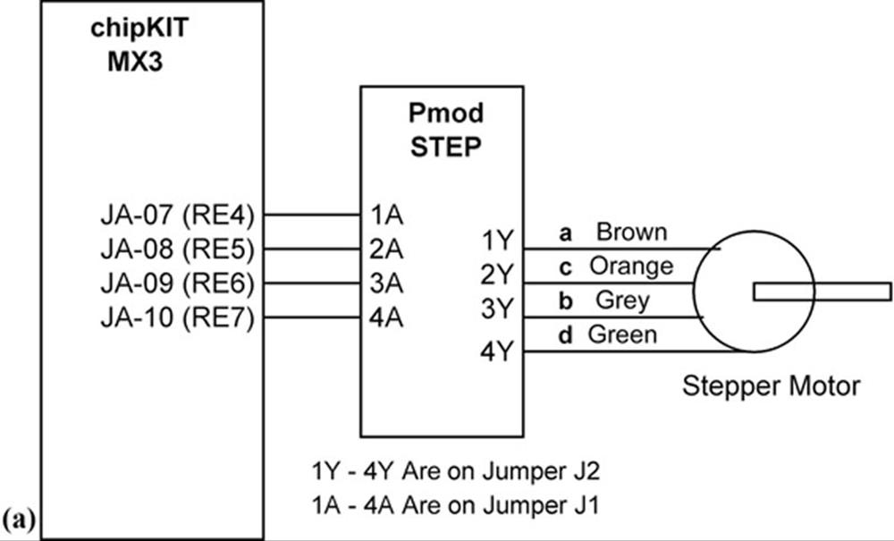
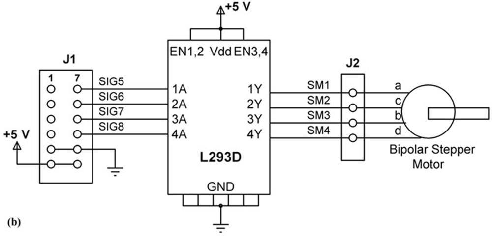
FIGURE 7.198 (a) Circuit Diagram of the Project. (b) Pmod Connections
7.34.3. Project PDL
The project PDL is shown in Figure 7.199. At the beginning, the I/O pins connected to the motor are configured as outputs. Inside the main program loop, the motor is rotated three revolutions in one direction, then stopped for 5 s, and then rotated three revolutions in the other direction, and is then stopped.
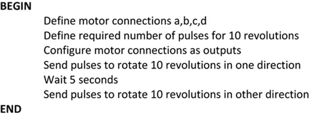
FIGURE 7.199 Project PDL
7.34.4. Project Program
The program is called MOTOR, and its listing is shown in Figure 7.200. Inside the setup() routine, the required number of revolutions and number of pulses required to obtain these revolutions are specified. Since the motor stepping angle is 1.8°, the number of pulses to be sent to the motor to make the motor turn REV revolutions is calculated as (200 × REV)/4. Two functions are used to rotate the motor. Function Forward sends pulses (see Table 7.17) to PORTE in the following order to rotate the motor forwards. A small delay (5 ms) is used between each pulse. This delay determines the speed of rotation:
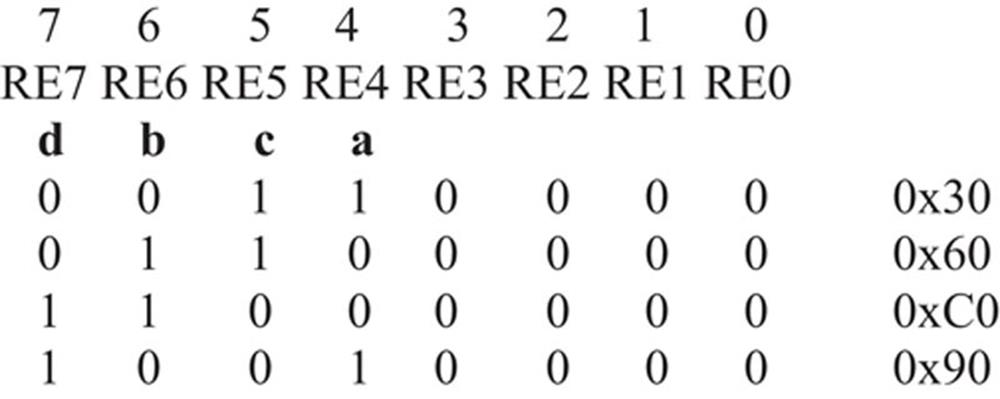
In order to rotate the motor in the opposite direction, the pulse order must be reversed. Function Reverse sends pulses (see Table 7.17) to PORTE in the following order to rotate in the reverse direction. A small delay (5 ms) is used between each pulse. This delay determines the speed of rotation:
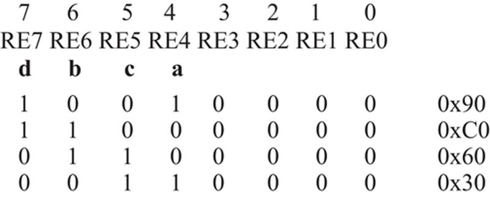
You should see the four LEDs E–H flashing as the motor is rotating.
All materials on the site are licensed Creative Commons Attribution-Sharealike 3.0 Unported CC BY-SA 3.0 & GNU Free Documentation License (GFDL)
If you are the copyright holder of any material contained on our site and intend to remove it, please contact our site administrator for approval.
© 2016-2026 All site design rights belong to S.Y.A.