Practical Electronics: Components and Techniques (2015)
Appendix A. Essential Electronics and AC Circuits
This appendix presents brief overviews of specific topics in basic electronics theory, beyond the discussion presented in Chapter 1. It is intended for anyone who might be interested in exploring some of the theory behind electronics, or who perhaps might benefit from it for personal projects. Topics covered include voltage, current, power, series and parallel circuits, Thévenin circuit analysis, capacitance, and impedance. A terse overview of basic solid-state theory is included to introduce the concepts of semiconductors and their applications.
Appendix B contains a set of basic electronic schematic symbols. If you encounter something here that you don’t recognize, be sure to look there. If you need more information than what is contained here, then you might want to look into the texts listed in Appendix C.
The main emphasis throughout this appendix is on the fundamental concepts, rather than the details. With a good grasp of the fundamentals, you’ll find the more detailed concepts behind modern electronic components and circuits much easier to comprehend. So think of this appendix as a travel brochure to the land of electronics. What adventures you decide to have beyond this point are entirely up to you.
Units of Measurement
Table A-1 lists some of the most common characteristics that apply to electrical circuits. These will appear throughout the rest of this appendix as they are needed, and they are defined in Chapter 1, here in the appendix, and in the Glossary.
|
Unit name |
Symbol |
Reference |
Measurement |
|
Ampere |
A |
I |
Electric current |
|
Coulomb |
C |
Q |
Electric charge |
|
Farad |
F |
C |
Capacitance |
|
Henry |
H |
L |
Inductance |
|
Hertz |
Hz |
f |
Frequency |
|
Joule |
J |
E |
Energy |
|
Ohm |
Ω |
R |
Resistance |
|
Seconds |
s |
t |
Time |
|
Volt |
V |
E |
Voltage |
|
Watt |
W |
P |
Power |
|
Table A-1. Standard units of measure used in electronics |
|||
In Table A-1, the Symbol column gives the nomenclature used with a definite value: 1V, 2.5A, 1 second, and so on. The Reference column gives the letter typically used in equations and schematic component references, as in C1, R10, E = IR, and so on.
In many cases, a fundamental unit of measure is impractical for normal usage, so it is specified in larger or smaller units through the use of a prefix. Table A-2 lists the most commonly encountered unit prefixes.
|
Prefix |
Symbol |
Multiplier |
Meaning |
|
giga |
G |
1 x 10⁹ |
one billion |
|
mega |
M |
1 x 10⁶ |
one million |
|
kilo |
k |
1 x 10³ |
one thousand |
|
milli |
m |
1 x 10⁻³ |
one thousandth |
|
micro |
μ |
1 x 10⁻⁶ |
one millionth |
|
nano |
n |
1 x 10⁻⁹ |
one billionth |
|
pico |
p |
1 x 10-12 |
one trillionth |
|
Table A-2. Standard value prefixes used with electronic units of measurement |
|||
Resistance is seldom given in milliohms or smaller, although these can occur when you’re working with precision measurements of low values of resistance in the laboratory. You will usually see ohms given as kilo ohms, mega ohms, or just ohms, and values less than 1 ohm are usually given as a decimal value. Capacitance and inductance, on the other hand, are most often given in micro, milli, nano, or pico units.
Voltage, Current, and Power
The two key characteristics of electrical phenomena are voltage and current. Voltage can be viewed in several ways. The most common is to treat it as being analogous to pressure. Voltage can also be viewed as a type of potential energy. The third way is to view voltage as the measure of the electromotive force behind electron movement. Current is analogous to flow volume and is defined as the number of electrons moving past a particular point in a circuit in a specific interval of time.
The two concepts are closely related, and it is not always possible to speak of one without reference to the other. Without voltage, no current can flow, and without current flow, there is static electrical charge (a voltage), but no meaningful work can occur.
Refer to Chapter 1 for an overview of electric charge and electron movement. Many of the terms and concepts used here are defined there, so I won’t duplicate that effort.
In a DC circuit, the relationships between voltage, current, and power are straightforward. There are no time, phase, or frequency aspects to worry about, as in the case with AC circuits. “AC Concepts” looks more closely at AC circuits, but in general, the discussion here about voltage, current, and power also applies to AC (with some frequency-dependent exceptions, which are covered in “Capacitance, Inductance, Reactance, and Impedance”). Current is discussed in “Current”, and power is covered in “Power”.
Voltage
The unit of measure for voltage is the volt, abbreviated as V. In a DC circuit, voltage can be defined simplistically as the electric potential difference between two points.
In an electric circuit, energy is put into a system and either does some work, such as being converted to heat, or is expressed as electical or magnetic fields, as in the case of AC circuits and reactive components. The main point is that in order to create the potential gradient, something had to expend some energy in some fashion. That energy is returned when the potential becomes a voltage drop across a component and current flows. If the component is a resistor (or even just a wire), it will be expressed mainly as heat. If it is an inductor, the energy is stored in the magnetic field that forms around the coils of the inductor (or around a single wire). A capacitor stores energy in the form of an electric field between two plates. “Capacitance, Inductance, Reactance, and Impedance” covers inductors and capacitors in more detail.
Another way to view voltage when current is flowing is as the force pushing current flow. The higher the voltage, the more readily it will force current flow through an impediment such as resistance (or an insulator, if the voltage is very high). By the same token, as the voltage or current is increased, more energy will be expended in the process, which is expressed as power, usually in the form of heat.
The amount of voltage between two points in an electric circuit is dependent on the voltage source, which itself applies some type of force to produce a current flow. A generator or dynamo uses electromagnetic force (EMF) to produce current flow at a given voltage. A power supply converts the voltage and current from a common AC power circuit (for example) into a specific voltage with a particular available current in either DC or AC form. A battery uses an electrochemical process to produce the electromotive force to generate a voltage potential.
Figure A-1 illustrates the three forms of voltage. A source of electromotive force produces a potential voltage. The EMF source might be a battery, a generator (dynamo), a bimetallic junction, or a solar cell. Whatever it is, it is a primary source of electrons with some amount of EMF giving them a potential voltage. This initial generation of EMF involves the conversion of some form of energy (chemical, electromechanical, thermal, or photonic) into electrical energy.
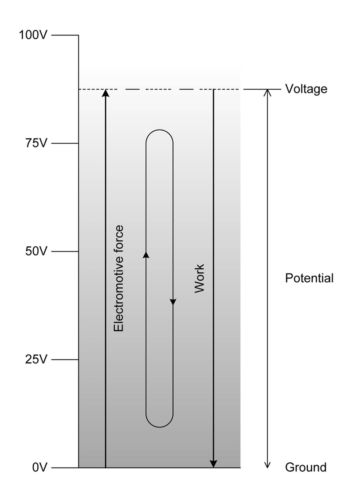
Figure A-1. Voltage potential and EMF
So long as the potential remains untapped, it will simply be a static potential. It is described in terms of volts, but not current or power (since it is static, no electrons are moving). When the potential is converted into current flow in a closed circuit, then the concepts of current and power come into the picture. The downward-pointing arrow in Figure A-1 indicates the drop in potential as current flows, some work is done, and the potential difference decreases back to zero. The voltage level shown is arbitrary and is solely for the purpose of illustration.
Figure A-2 shows a graphical representation of a DC voltage over time, which is just a straight horizontal line across the graph. This is what you would expect to see if you looked at a DC voltage with an oscilloscope. Again, the voltages were selected for illustration purposes.
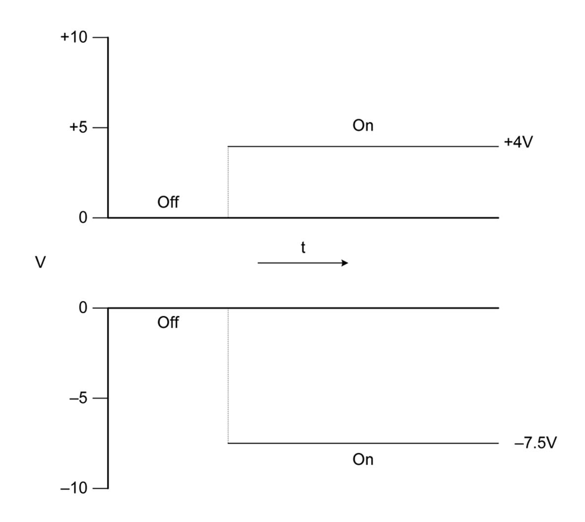
Figure A-2. DC voltage over time, a straight line
Notice that Figure A-2 shows both positive and negative voltages. The polarity of a DC voltage is largely dependent on what is used as the neutral (i.e., ground) reference; and in some cases, the positive terminal of a power source might be ground, in which case the voltages measured in the circuit would be negative. Some types of power supplies have both positive and negative outputs. This is often the case in PC power supplies, like the one described in “Power”.
It’s important to bear in mind one essential fact about voltage: it exists only relative to two specific points. In other words, voltage is measured relative to something. When a voltage is measured relative to a common reference point (e.g., ground), it is a measure of the circuit voltage at that point. It doesn’t really say anything about voltages across individual components, only how the circuit has affected the voltage at the measurement point (if there has been any effect at all).
Figure A-3 illustrates the measurement concept. Assuming that R1 and R2 are the same value, the voltage at point A will be some fraction of the supply voltage, which is shown as one-half of the supply voltage in this case. The actual value of the voltage at point A will depend on the values of R3, R4, and R5. Refer to Chapter 1 for an introduction to voltage dividers and to “Series Resistance Networks”, “Parallel Resistance Networks”, and “Thévenin’s Theorem” for a more detailed discussion of series and parallel resistance networks. The voltage at point B will always be whatever the supply voltage happens to be, which is 9V in this case.
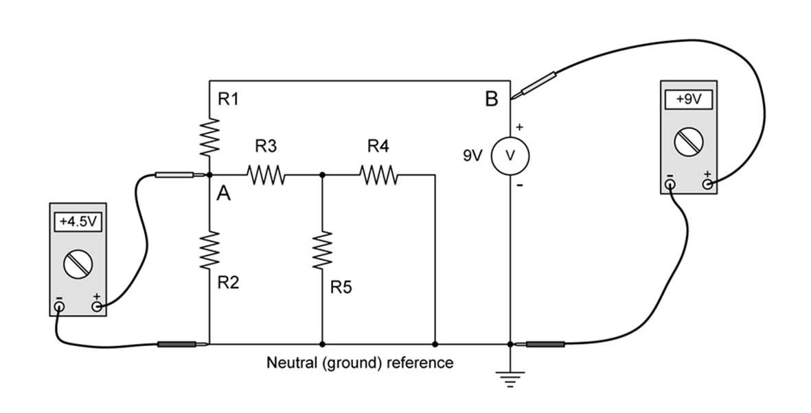
Figure A-3. Voltage measurement in a circuit
The voltage measured across a component is called the voltage drop. Figure A-4 employs the circuit from Figure A-3 to illustrate this distinction.
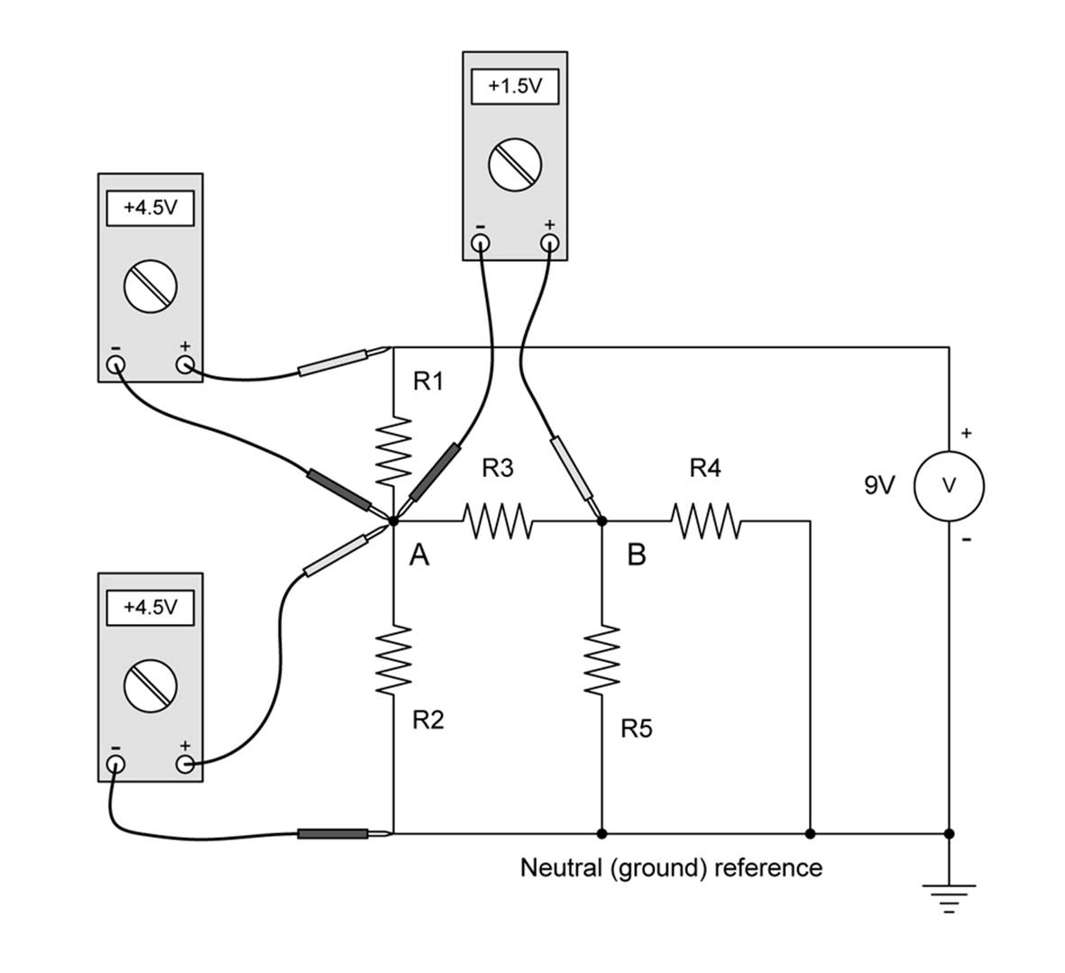
Figure A-4. Voltage drops in a circuit
The voltage measured across R3 (between points A and B) in Figure A-4 is the voltage drop across the resistor, as is the voltage across R1. The measurement from point A to neutral across R2 is the voltage drop across R2.
Current
Current flow is one of the two essential features of electricity (the other being voltage). Electrical current is the movement (or flow) of electrical charge through a conducting medium of some sort. Although it is typically used to refer to electrons as the charge carriers, it can also describe the flow of charge carried by ions within the electrolyte of a battery, for example. In principle, anything that carries electrical charge from one point to another is a form of current flow. It is analogous to the volume of fluid flowing through a pipe in, say, liters per second, or the number of steel ball bearings moving past a point in a tube in some specific interval of time (borrowing from Chapter 1). Electrical charge without current flow is just static charge and does no work.
Current is measured in amperes, abbreviated as A, and often shortened to amp. The quick and easy definition of current states that one ampere of current can be defined as 1 coulomb of charge (6.24 × 10¹⁸ electrons) moving past a given point in an electric circuit per unit time, although the traditional formal definition involved the force generated between two conductors spaced some fixed distance apart in a vacuum. Recently, it has been proposed that the formal definition adopt the more straightforward definition, wherein 1 ampere is defined as 6.2415093 × 10¹⁸ elementary charges (either positive or negative) moving past a specific point in one second of time. Or, to put it another way:
1 ampere = 1 coulomb per second
Power
Electrical current is used to perform work of some kind. This might be in an electric motor or a loudspeaker, wherein the current flow and associated electromagnetic phenomena are converted to mechanical motion. It could also be in the form of an incandescent lamp, a solid-state circuit (e.g., a radio or a computer), or an electric arc welder. In each case, the flow of electrons performs some type of work, with the result typically expressed as heat, radiant electro-magnetic energy (RF), mechanical motion, or a combination of all three.
Power is a measure of energy expended as work is performed. Electrical power is simply the product of voltage and current, in that P = EI, where P is the power, in watts, E is the voltage, and I is the current, in amperes. From this, you can see that something like an electric arc welder operating at 25V (with the arc active) at 150A of current will produce 3,750W of power at the arc, all of which is concentrated into a small area about 1/8 inch to 1/4 inch in diameter. It’s no wonder that it can melt metal.
Conversely, the power supply in a typical vacuum tube (valve) audio amplifier might produce 500V DC at around 250 mA (milli-amperes). This results in 125W of available power. So, although the current is low, the high voltage is what gives the amplifier power to easily produce 25W or more of audio output to drive the loudspeaker.
Lastly, consider the switching-mode power supply (SMPS) in a modern PC. The input voltage and current are 8.5A at 115V RMS, which is 977.5W (“AC Concepts” discusses RMS). Table A-3 shows the output specifications for a typical low-cost PC power supply.
|
Output (V) |
Current (A) |
Power (W) |
|
+3.3 |
20 |
66 |
|
+5 |
20 |
100 |
|
+12 |
18 |
216 |
|
+12 |
18 |
216 |
|
-12 |
0.8 |
9.6 |
|
+5 |
2.5 |
12.5 |
|
Table A-3. Output specifications for a typical low-cost PC power supply |
||
The supply is rated for 400W, so that implies that the specifications might be a bit misleading. If you add up all the output power, we get 620.1W. If you assume that one of the +12V outputs is simply a duplicate of the other and subtract 216W, then you get 404.1, which is close to the manufacturer’s stated rating. Notice that there is a significant difference between the input power and the available output power. Some simple math (output/input × 100) shows that the supply is approximately 41% efficient. This isn’t great, as a switching-mode power supply can do better than that, but it’s acceptable for something around $40. The real downside here is that the wasted power (around 573 watts) is going to end up as heat, so the fan in this unit will be running quite a bit when it’s under load.
Resistance
In DC circuits, the thing that mediates the relationships between voltage, current, and power is resistance, or resistivity, and its reciprocal, conductivity. In AC circuits, capacitance, inductance, and reactance also come into play, and those are discussed in “Capacitance, Inductance, Reactance, and Impedance”. However, in an AC circuit with no significant amount of inductance or capacitance, the concepts presented here for DC circuits will generally apply to root mean square (RMS) values for AC voltages (see “AC Concepts” for the definition of RMS).
Conductivity and Resistance
Electrical conductivity is a characteristic of all physical matter. The degree of conductivity ranges from zero (a perfect insulator) to infinity (a perfect conductor). The actual numeric value of conductivity can range from a very small number (for an insulator), to a very large value (for a good conductor).
The reciprocal of conductivity is resistance, which is what is normally used when we are considering the resistivity of a component. For example, a component with a resistance of 1 ohm has a conductivity of 1, whereas a component with a resistance of 1,000,000 ohms has a conductivity of 0.000001. A component with a resistance of 0 has an undefined (infinite) conductivity. From this, it follows that no matter how good a conventional conductor might be, it will never have infinite conductivity, and hence it will always have some amount of resistance. The only known exceptions are superconductors.
In electrical circuits, a resistor is a component that is designed to exhibit a specific resistivity. One way to consider this involves the concept of valence electrons presented in Chapter 1. Elements that can easily give and accept valence electrons tend to be good conductors, and consequently have a relatively low resistance to current flow. Those elements that have tightly bound electrons tend to be poor conductors, and hence good insulators. Resistors lie somewhere between insulators and good conductors and are made from various forms of carbon, high-resistance wire, and vapor-deposited films, among other materials. The material type and thickness are adjusted to produce the desired resistance value. Chapter 8 describes the various types of resistors that are available.
When current flows through a resistance, work is done to maintain the current flow. The higher the resistance (and the lower the conductivity), the higher the level of work necessary to maintain a given current flow. Varying the voltage across the resistive load will vary the amount of currentpushed through the load. The relationship between voltage, current, and resistance is defined by Ohm’s law.
Ohm’s Law
We can use the relationship defined by Ohm’s law to help understand how voltage, current, and resistance interact, and subsequently, how power is related to these three characteristics as well.
Ohm’s law is stated as:
![]()
where E is the voltage in volts, I is the current in amperes, and R is resistance in ohms. The use of the symbols E and I is largely a matter of historical legacy. You can replace them with V and A if you wish, and some people do, but the old-school form is the one most widely recognized.
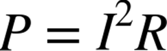
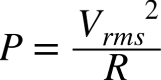
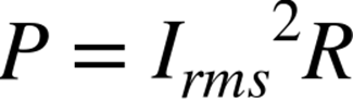
A load in an electrical circuit will have a specific resistance. If you know the resistance, it is possible to calculate the current at a given voltage. Once the current is known, you can calculate the power using the relationship given in “Power”:
![]()
Ohm’s law and the power equation are linear relationships, but in real applications, there are things like the power source current limit, load power handling capacity, and other factors to take into account that might limit the range of linearity. How a power source will behave when it reaches its current limit depends on the type of the source. In many cases, it will simply not generate any higher voltage once the current limit is reached. How a load will respond when its power dissipation limit is reached or exceeded depends on the nature of the load. It might melt, burst into flames, or simply become an open circuit and cease to conduct.
Now, let’s have some fun with the power equation and Ohm’s law. We can derive a useful variant of the power equation by simply replacing the E term with IR, which results in:
Substituting E/R for I in the original equation yields another useful variation:
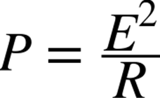
So, if you know the resistance and the current, you don’t really need to know the voltage drop in order to calculate the dissipated power. Or if all you know is the voltage drop and the resistance, you can still calculate the power using the second form.
Series Resistance Networks
Resistors can be arranged in series or parallel circuits to create new values and power handling capacity. This is useful when the value needed simply isn’t available, but a lot of the wrong parts are on hand. It is also useful when a resistance needs to be able to handle a certain amount of power, but no such part is on hand (or might not even be readily available). A collection of resistors connected in series or parallel, or both, is commonly referred to as a resistance network.
When connected in series, the values of some number n of resistors (where n > 1) sum, as shown in Figure A-5.
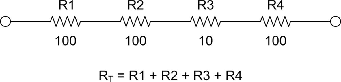
Figure A-5. Resistors in series
Note that in a series network, the amount of current flowing through each resistor is the same. You can calculate the voltage drop across each resistor, and hence the amount of power it will dissipate, by treating the series network as a multi-tap voltage divider, as shown in Figure A-6.
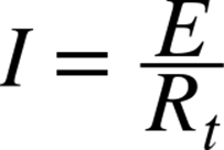
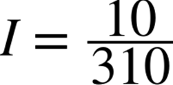
The first step is to sum the values of the resistors to get Rt and then use the supply voltage (10V) to determine the total current through the network. In this case, it works out to 0.03226A (32.26 mA):
![]()
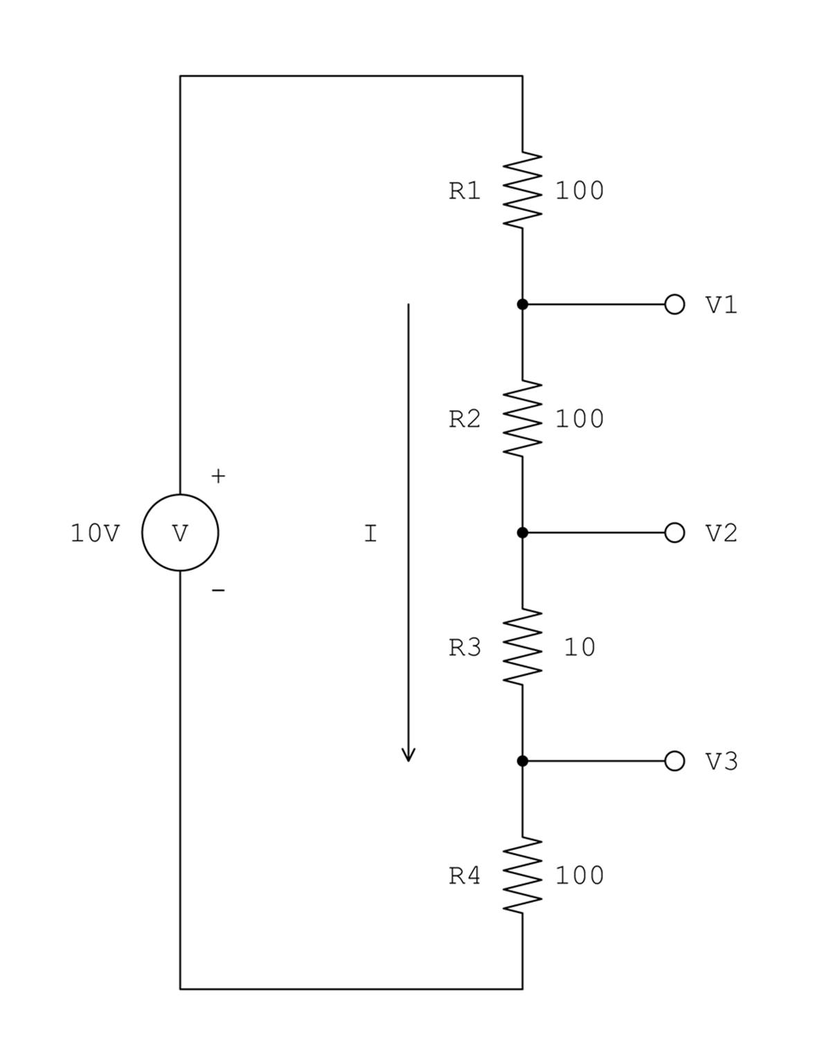
Figure A-6. Series resistance network as a multi-tap voltage divider
The next step is to sum the values of R2, R3, and R4, which gives 210 ohms. You can now treat the network as a two-resistor voltage divider and use Ohm’s law to find the voltage for V1. This turns out to be:

Next, sum R1 and R2 to get 200 ohms, and R3 and R4 to get 110 ohms. Again apply Ohm’s law to derive V2:

Finally, just use the value of R4 to get V3, which gives you:

Now that you have V1, V2, and V3 (which have been rounded appropriately), you can work out the voltage drops across each resistor in the network, as shown in Figure A-7.
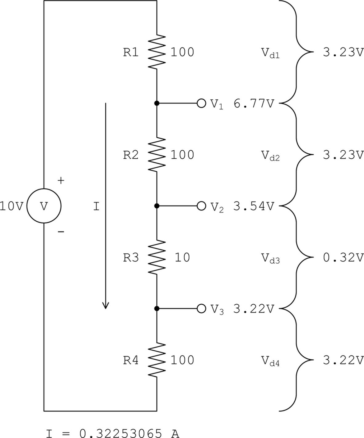
Figure A-7. Series resistance network voltage drops
As a sanity check, you can sum up the voltage drops and verify that they are equal to 10V:


Finally, you can apply the voltage drops to determine what the power dissipation will be for each resistor, as shown in Table A-4. Remember that the network current is 0.03226A through each resistor, so the power is simply the voltage drop times the network current.
|
R |
V drop |
Power (W) |
|
R1 |
3.23 |
0.104 |
|
R2 |
3.23 |
0.104 |
|
R3 |
0.32 |
0.01 |
|
R4 |
3.22 |
0.104 |
|
Table A-4. Calculation of power dissipation in a series network using voltage drops |
||
The sum of the power values for Table A-4 is 0.322W.
The alternative approach, which is more straightforward but not as accurate, is to use the alternate I2 form of the power equation. Since you know that the current in a series network is the same through all of the components, and you know the resistance values, calculating the power dissipation for each resistor is simplicity itself. Table A-5 list the results.
|
R |
Power (W) |
|
R1 |
0.104 |
|
R2 |
0.104 |
|
R3 |
0.01 |
|
R4 |
0.104 |
|
Table A-5. Calculation of power dissipation in a series network using P = I2R |
|
The sum of the power values for Table A-5 is 0.322W, which is the same as the preceding calculation.
Parallel Resistance Networks
A parallel configuration reduces the total resistance of the network, as illustrated in Figure A-8.
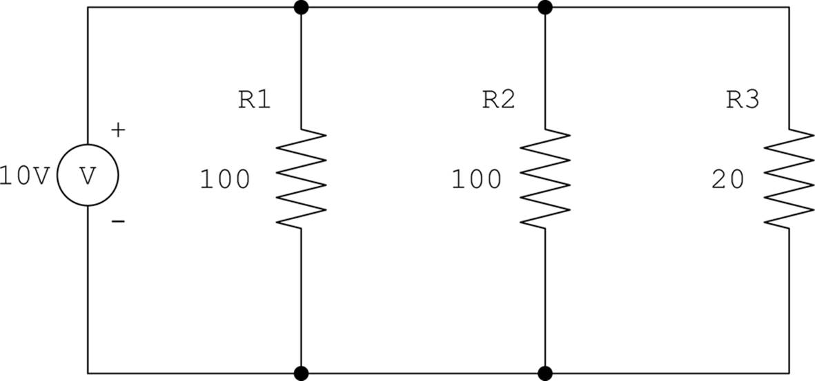
Figure A-8. Resistors in parallel
The total resistance of a parallel resistance network with more than two elements is given by:
For two parallel resistors, you can use:
If n resistors in parallel have the same value, the equivalent resistance is just the value of any one of the resistors divided by the number of resistors in parallel:
In order for this to work, the resistive elements must have the same value. If they are different values, you’ll need to use one of the other equation forms to compute the total resistance of the parallel network.
In a parallel network, the voltage across each resistor is the same, but the current through each depends on the resistance of the component, and sums into the total current for the network:
Figure A-9 shows how each component in a parallel resistance network can have different amounts of power dissipation. In this case, there are three resistive loads, perhaps lights or maybe heating elements. Although the voltage across all three is the same, the amount of current flowing through each differs based on its resistance.
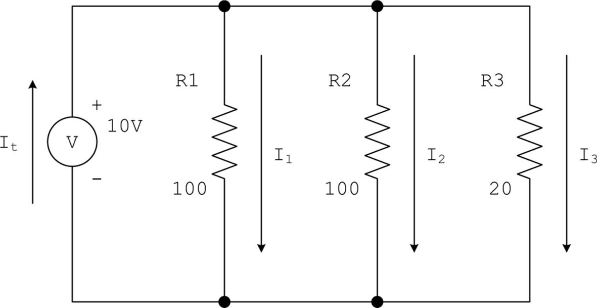
Figure A-9. Current flow in a parallel resistance network
To calculate the power, you can use the P = I2R form of the power equation, because the loads are in parallel and each can be dealt with separately from the other elements in the network. Using 10V as the supply voltage, you can determine the current for each using Ohm’s law. Once the currents are known, P = I2R calculates the power dissipation for each resistor. Table A-6 shows the results of the math.
|
Load |
Current (A) |
Power (W) |
|
R1 |
0.1 |
1 |
|
R2 |
0.1 |
1 |
|
R3 |
0.5 |
5 |
|
Table A-6. Calculation of power dissipation in a parallel network using P = I2R |
||
The total current demand on the power source will be 0.7A, with a total power dissipation of 7W. The I2 form of the power equation is a good choice here, because in a parallel network, the voltage drop across each component is the same. What varies is the amount of current flowing through each load element.
The sanity check for Figure A-9 is simply to compute the parallel resistance of the network and derive the total power from that:
This gives an Rt of 14.285714286 ohms. Using I = E/R, you find that the total current would be 0.7A, and P = EI gives 7W of power. This is the same as the It of 0.7A and the 7W obtained from Table A-6. Note that, while this is a valid answer, it does not tell you the power dissipation for the invidual resistors in the network, whereas the first form does.
Equivalent Circuits
When dealing with complex circuits, it is sometimes useful to represent the circuit in a simpler form. These representations are referred to as equivalent circuits, because they are a simplified version of what might otherwise be a very complex circuit.
The simplest DC circuit consists of a power source and a load element (e.g., the battery and light bulb from Chapter 1). The power source produces some amount of current at a given voltage. The current flows through the load and power is dissipated in some form, typically heat. Working with a simple circuit like this is much easier than trying to deal with the interactions within a complex circuit.
The use of equivalent circuits allows you to focus on the key characteristics of a circuit or system without becoming mired in the details. One way to think of an equivalent circuit is as a black box that has some particular characteristics (voltage, current, and resistance) but whose internal details are hidden from view, since they don’t really matter from the perspective of whatever the black box happens to be connected to in the circuit.
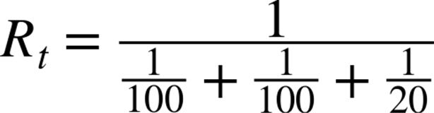
Voltage and Current Sources
In its most common form, an equivalent circuit is composed of passive, linear elements. In addition to the common symbols for resistors, capacitors, and inductors, a variety of symbols are employed with equivalent circuits to indicate voltage and current sources. You have encountered only a voltage source so far. Figure A-10 shows a more complete set.
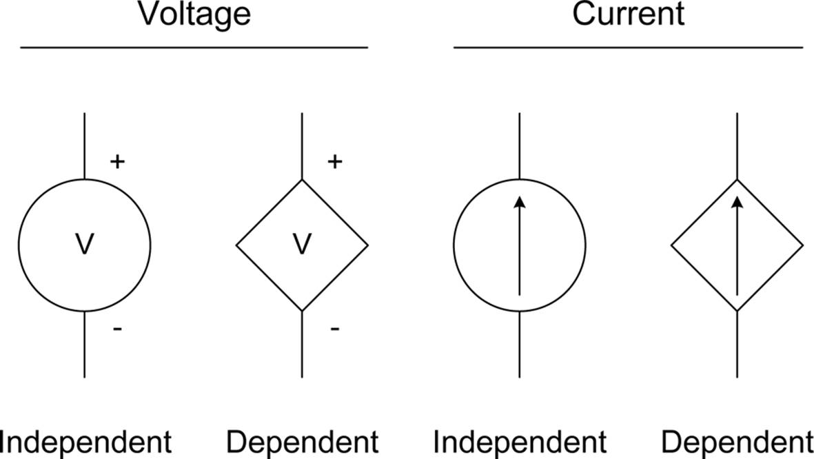
Figure A-10. Symbols used in equivalent circuit diagrams
Note that there are two types for both voltage and current: independent and dependent. An independent source is not affected by changes in the connected network, while a dependent source will change according to variables in the connected network. You might think of a dependent source as having a knob or lever that something else can use to alter its output. It is the dependent sources that allow an equivalent circuit to model an active circuit element like a transistor or operational amplifier.
Lumped-Parameter Elements
Equivalent circuits are simplifications of more complex circuits and are composed of lumped-parameter elements, wherein something like a resistor in an equivalent circuit might represent many resistors (and other components) in a complex network (e.g., a Thévenin equivalent). This applies to capacitors and inductors as well (discussed in “Capacitance, Inductance, Reactance, and Impedance”). The main point of an equivalent circuit is to model the behavior of a more complex circuit by retaining the essential electrical characteristics of the original circuit in a simplified form that aids analysis.
Thévenin’s Theorem
Thévenin’s theorem states that any linear electrical network (complex circuit) that is composed of only voltage sources, current sources, and resistances can be represented by an equivalent voltage source and an equivalent resistance. When dealing with AC circuits, you can apply Thévenin’s theorem to reactive impedances at some given frequency (see “Capacitance, Inductance, Reactance, and Impedance” for more on reactive components).
Thévenin equivalent circuits are useful for analyzing power systems with variable loads. For example, a power source might have a complex internal circuit, but its Thévenin equivalent will have an equivalent behavior, which is much easier to work with. Another application involves the simplification of a set of circuits in a larger system so that each subcircuit can be represented by its equivalent.
Figure A-11 shows how a simple circuit with a voltage source and five resistors can be represented by an equivalent circuit with just a single voltage source and one resistor. From the perspective of nodes A and B, both the original and the equivalent would appear to be identical. Deriving a Thévenin equivalent is really nothing more than utilizing Ohm’s law and the concepts of series and parallel resistances that were covered earlier.
Figure A-11. Thévenin equivalent circuit example
When you are converting a circuit to its Thévenin equivalent, the first step is to deal with the voltage and current sources. Under normal conditions, a source will have some amount of internal resistance, usually rather low. You can elect to ignore this and treat the voltage and current sources as ideal sources. An ideal voltage source is replaced with a short circuit, and an ideal current source is replaced with an open circuit.
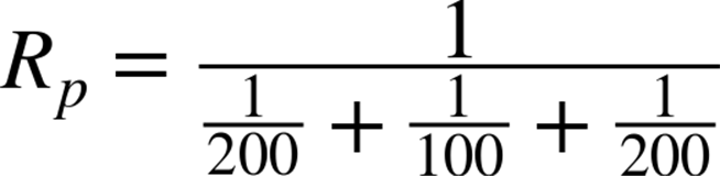
In order to define the equivalent circuit, you will need the equivalent voltage and resistance. For this example, let’s pick some arbitrary values:
§ R1 = 100 ohms
§ R2 = 100 ohms
§ R3 = 200 ohms
§ R4 = 100 ohms
§ R5 = 200 ohms
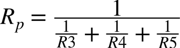
The first step is to determine the value of the parallel network composed of R3, R4, and R5:
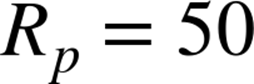
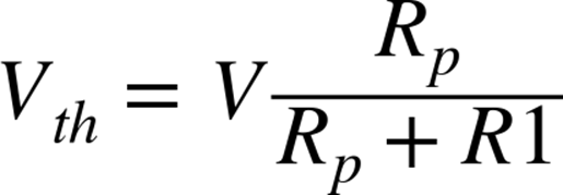
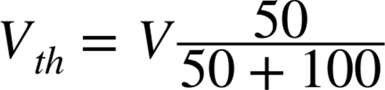
The Thévenin-equivalent voltage (Vth) is the voltage at the output terminals A and B of the equivalent circuit. In this case, I’ve elected to treat the circuit as a voltage divider. This arrangement is shown in step 2 of Figure A-11. R2 is ignored on purpose. Since this is an open circuit calculation, there is no current flow through R2, and hence no voltage drop.
Now you can determine the open circuit voltage at point C (Vth) in the circuit:

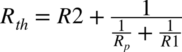
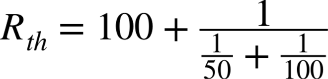
The Thévenin-equivalent resistance is the resistance measured across points A and B of the circuit. To calculate the equivalent resistance, replace independent voltage sources with short circuits, and independent current sources with open circuits. This is shown in step 3 of Figure A-11, where the sole voltage source has been replaced with a short circuit. This is equivalent to R1 and Rp in parallel, and R2 is now included in the calculation:
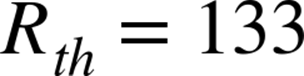
The result of our effort is shown in step 4 of Figure A-11, and Figure A-12 shows the final result.
Thévenin equivalent circuits are not perfect representations, and they have some limitations. The first involves linearity. Many circuits are linear only over a specific range, so the Thévenin equivalent is valid only within that range. Secondly, a Thévenin equivalent might not accurately model the power dissipation of the actual complex circuit. Still, even with these caveats, Thévenin’s theorem is a handy tool to help you understand complex electrical circuits.
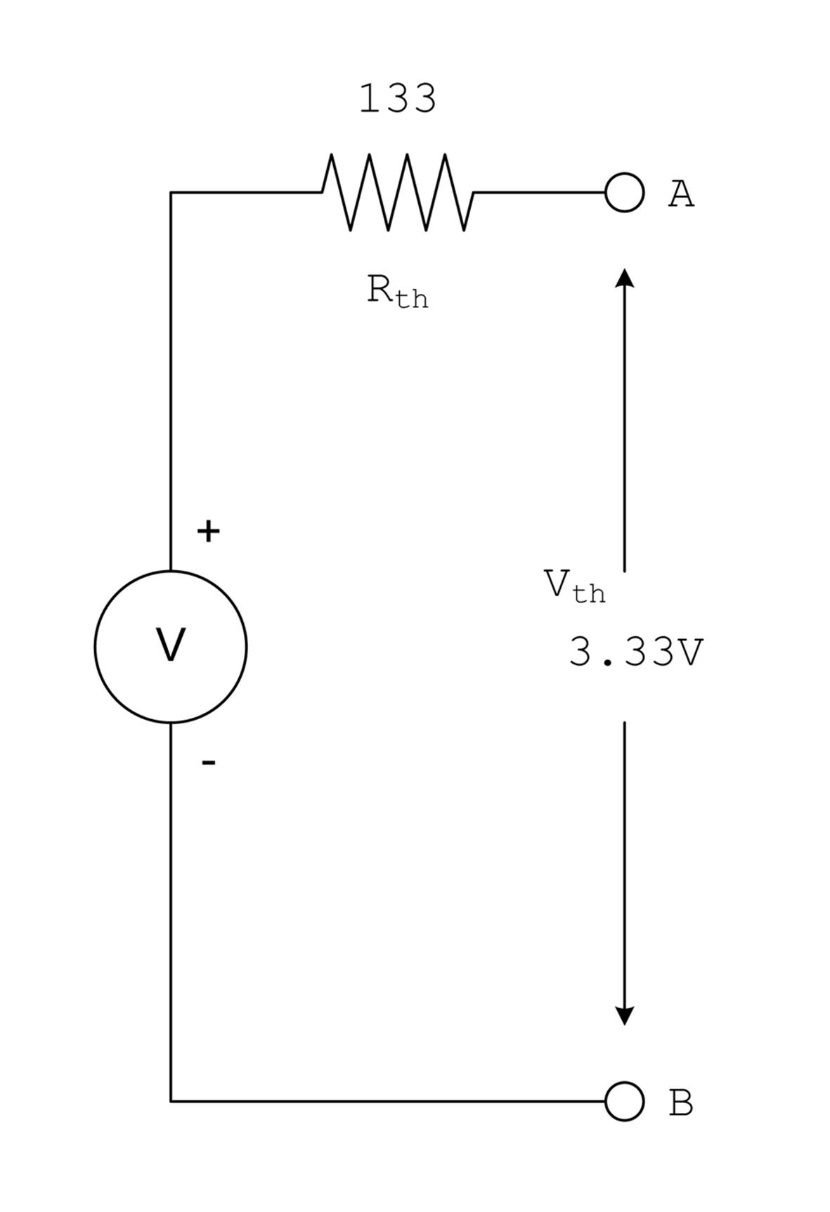
Figure A-12. Final Thévenin equivalent circuit result
Equivalent Circuit Applications
Equivalent circuits are useful for more than just passive components. The linear behavior of active components such as transistors and op amps can be modeled with equivalent circuits and dependent sources. For example, Figure A-13 shows a simple model of an ideal op amp.
In Figure A-13, the idealized behavior is represented by the voltage output as a function of the voltage drop across the input resistance times the gain (G) of the device.
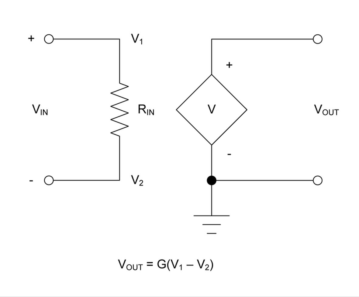
Figure A-13. An equivalent circuit example for an ideal op amp
In this form, this op amp equivalent can be dropped into an equivalent circuit model and treated like a resistor and a dependent voltage source. A simplified model like this is useful for a rough first-order analysis, and the level of detail can be increased as necessary to account for elements in the circuit such as a feedback path. “Operational Amplifiers” covers op amps.
Equivalent circuits simplify the analysis of the voltage and current characteristics of a circuit. This, in turn, allows you to make better decisions regarding circuit power handling, battery current capacity, and voltage requirements.
There are other circuit analysis techniques in addition to Thévenin equivalent circuits, such as Kirchkoff’s circuit laws and Norton’s Theorem. Since the objective of this section is just to provide a high-level look at equivalent circuits, they aren’t covered here. If you are inclined to learn more about equivalent circuits and circuit modeling, the texts listed in Appendix C describe these techniques in detail. Circuit simulation software such as PSpice (for Windows) also employs these techniques, and using a simulator is a lot less tedious than working out the equations by hand. Oregano and gpsim are examples of free analog circuit simulation software for Linux.
AC Concepts
Alternating current (AC), as the name implies, is a type of current flow that changes direction periodically. This is what makes it useful for power transmission, audio signals, and radio, but it also makes it more complicated. Whereas DC has only voltage as its primary characteristic, AC also has frequency, measured in hertz (Hz) or cycles per second, and phase, measured in degrees. In a sinusoidal waveform, such as the one shown in Figure A-14, a cycle is a complete waveform of 0 to 360 degrees, start to finish. AC also has a root mean square (RMS) value used to calculate power.
In most cases, the term AC refers to a sinusoidal waveform, as found with the mains current in many countries and shown in Figure A-14. Although you might think of something like the output of a signal generator producing a sine wave at, say, 1,000 Hz, as AC, that is more often referred to as a signal. The term AC is typically reserved for discussing power circuits, not signals, although they are the same thing and the fundamental concepts of AC circuits apply to both.
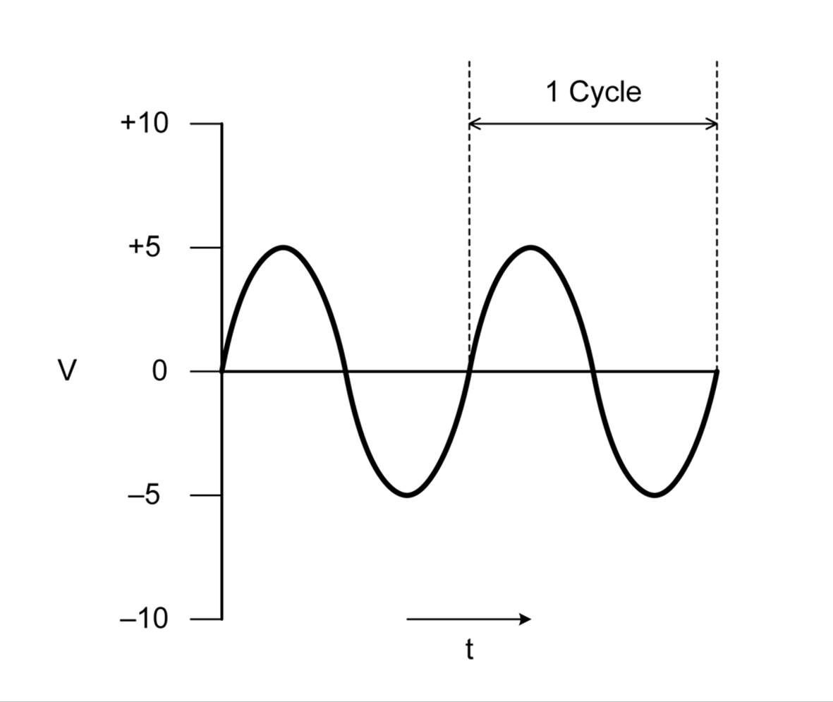
Figure A-14. AC voltage over time, a sine wave
The terminology associated with AC flow can sometimes be confusing and is dependent to a large extent on the context of usage. For example, when talking about the power wiring in a house, you would expect to hear AC, AC voltage, or AC current. These terms typically refer to the electrical power type in general, the voltage in the circuit, and the current flowing in the circuit, respectively. However, when referring to AC used to carry information (as is typically found in audio, radio, and instrumentation circuits), the common term is AC signal or just signal.
Alternating current has several unique primary features. As shown in Figure A-14, AC varies with time in a repeating cyclic fashion, the rate of which is its frequency. Frequency is the measure of the number of times the signal effectively changes direction in 1 second of time. Each time the voltage drops to zero, it is said to have reached a zero-crossing point.
Secondly, AC has both positive (high) and negative (low) peaks, but an RMS value is used for calculating power dissipation. Thirdly, AC has the characteristic of phase, measured in units of degrees from 0 to 360. Finally, with AC, the voltage and current can have different phases, which means that a peak in the voltage does not have to coincide with a peak in the current. This might seem counterintuitive at first, but it’s a result of the reactance of a capacitor or inductor, which is covered in “Capacitance, Inductance, Reactance, and Impedance”.
Waveforms
AC signals can occur with any one of a number of different types of waveforms, but the sine wave is the prototypical AC waveform. A sine wave is pure: that is, it comprises just one frequency. Other waveforms can be decomposed into a series of sine waves at various frequencies by means of Fourier analysis techniques (which we will not delve into here), but a pure sine wave cannot be decomposed any further. Figure A-15 shows a generic sine wave.
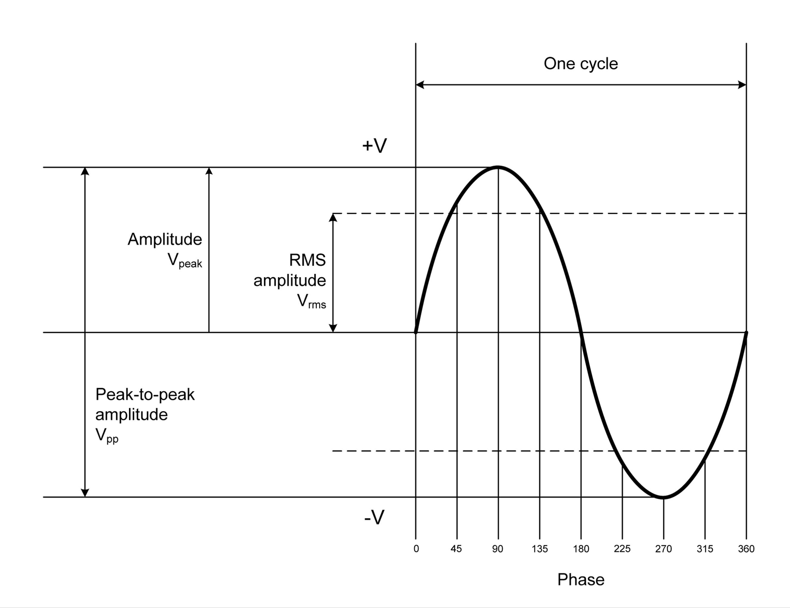
Figure A-15. Sine wave details
The sine wave gets its name from being defined mathematically by the sine function:
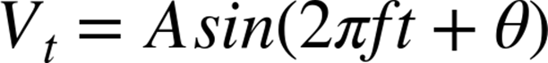
where A is the amplitude, f is the frequency, t is time, and theta is the phase. Sometimes, you might see this form:
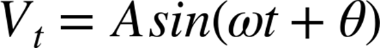
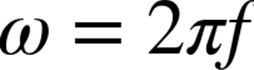
where omega, the angular frequency, is actually just:
The discussion of frequency, voltage, and power in “AC Frequency, Voltage, and Power” will refer back to Figure A-15.
Other Waveforms
Other periodic waveforms commonly encountered include square, triangle, pulse, and ramp, shown in Figure A-16.
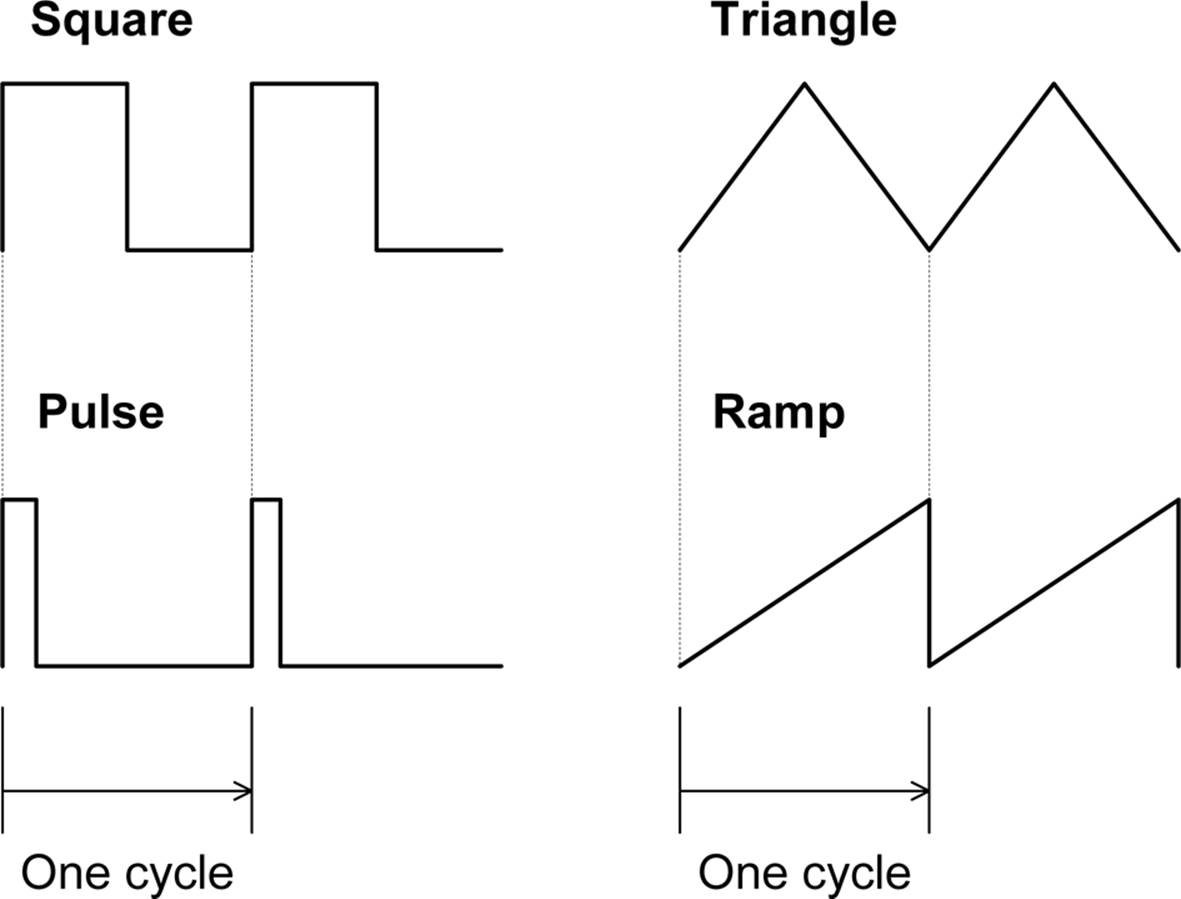
Figure A-16. Common types of electrical waveforms
Square and pulse waveforms appear mainly in digital logic circuits, because they easily represent the 1s and 0s of binary logic. The other waveform types appear in different contexts, such as power control circuits, timing circuits, music synthesis devices, and motion-control applications.
One of the most common, and most useful, of the nonsinusoidal waveforms is the square wave and its close relative the pulse. Although a square wave is usually drawn with a shape that implies instantaneous on and off times, in reality, square waves will include things like noninstantaneous rise and fall times, overshoot, and ringing, as shown in Figure A-17.
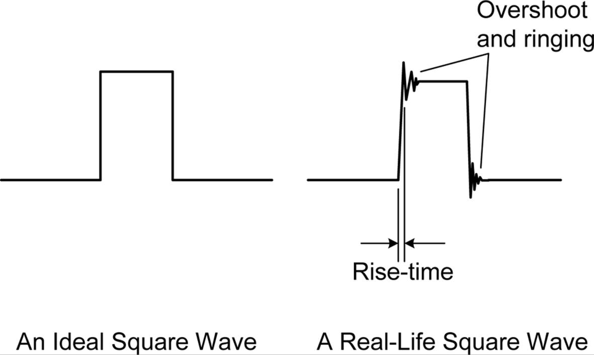
Figure A-17. Ideal versus real (typical) square wave
The overshoot and ringing occur because of the various inductance and capacitance effects in a circuit. Because even a wire has intrinsic inductance (as discussed in “Impedance and Reactance”), sending a pulse or square wave over more than a few feet of unshielded wire will result in a degraded signal at the receiving end.
When dealing with pulses and square waves, you’ll often hear references to the duty cycle of the waveform. In fact, a square wave is actually a special case of a pulse with a 50% duty cycle. That is to say, it is on for one-half of a cycle and off for the other half. Figure A-18 shows some pulses at various duty cycles.
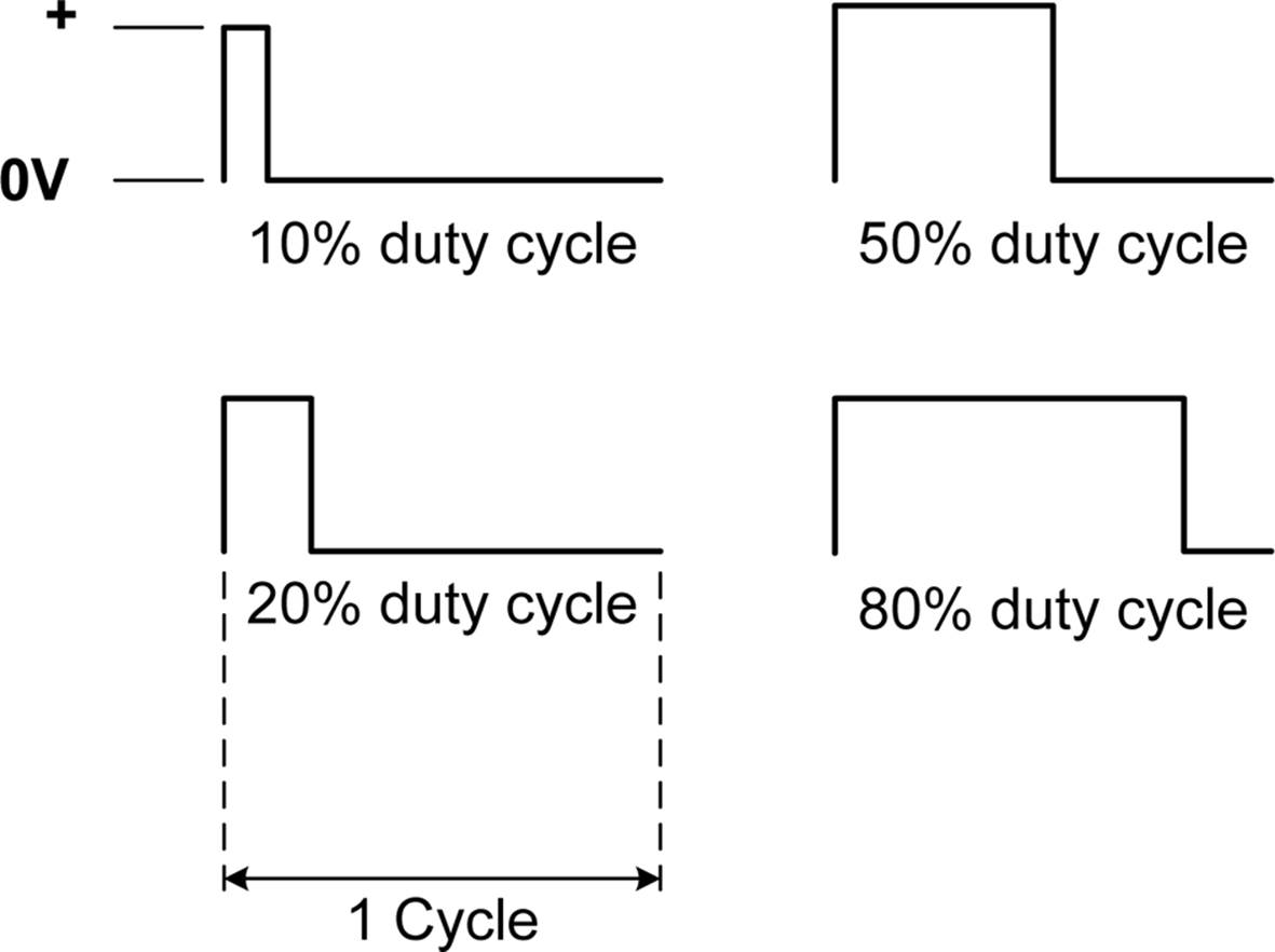
Figure A-18. Pulse duty cycle
AC Frequency, Voltage, and Power
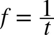
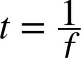
Every AC waveform has a frequency. The inverse of a signal’s frequency (f) is its period (t), which is the time interval between each repetition of the waveform:
This relationship applies to all periodic events, be it waveforms or the number of times a temperature sensor is queried in a given time interval. For example, if a video camera generates frames at a rate of 30 ms (milliseconds) per frame, it is operating at a frequency of 33.33 Hz. The time period of a 60 Hz signal is about 16.67 ms. A signal with a frequency of 10 KHz (10 kilohertz, or 10,000 Hz) has a time period of 100 μs (microseconds, sometimes written as u instead of μ).
Another essential characteristic is amplitude. There are three primary ways to describe the amplitude of an AC signal: peak amplitude, peak-to-peak amplitude, and RMS amplitude. Take a look at Figure A-15 again and notice that the peak value (the A term in the sine wave equations) refers to the maximum value on either side of the zero line. When we talk about the peak-to-peak value (often written as Vpp), we are referring to the range between the positive peak and negative peak.
Lastly, root mean square (RMS) amplitude is used to compute power (measured in watts, as with DC circuits) in an AC circuit. RMS is also known as the quadratic mean. For a sine wave Vrms = .707 * Vpeak, and for other waveforms, it will be a different value. You can think of RMS as an average of the Vpeak, and that is how it is used when computing power using:
and, conversely:
Now, here’s something to consider: the AC power in your house is probably rated at something like 120V AC (volts AC), and in some parts of the world, it might be higher. That is its RMS value. The Vpeak value is around 165 volts, and the Vpp is about 330 volts. The Vpp value isn’t really something to get excited about, but it might be useful to know that the actual Vpeak is 165 volts when you are selecting components for use with an AC power circuit. Just remember that the RMS value is used primarily to compute power.
AC Phase
The last primary characteristic to consider is phase, as shown in Figure A-15. If you consider how AC is generated electro-mechanically, you can see that the phase angle corresponds to the rotation angle in an AC generator (also called a dynamo or alternator). The primary phenomena behind an AC generator, electromagnetism, is covered in “Inductors”. The main focus here is phase. Figure A-19 shows a simplified diagram of a single-phase generator.
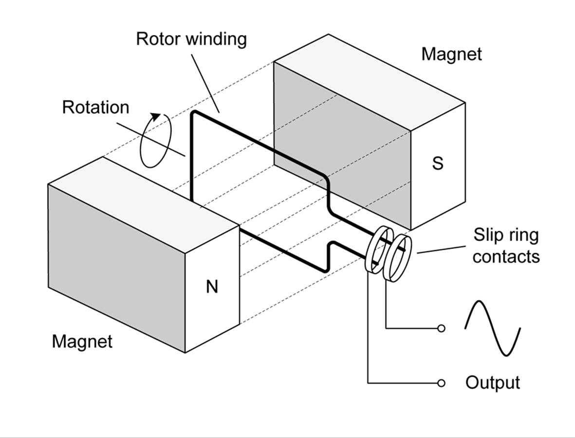
Figure A-19. Simplified AC generator
The output from the rotating coil between the magnets (the rotor) flows through a pair of slip rings. This allows for continuous contact with the rotor coil. As the rotor turns, the windings in the rotor intersect the magnetic field. This in turn causes current to flow. The direction of the motion of the windings relative to the magnetic field determines which direction the current will flow.
As the rotor in the generator turns, the output will vary at the same rate, with the result being a sine wave. The voltage of the output is a function of the angle of the rotor as it moves through the magnetic field produced by the stator assembly (and the number of windings in the rotor coil).Figure A-20 shows the phase angle relationship graphically. Note that the permanent magnets in this illustration (which are part of the stator and don’t move) are shown only once. The rotor is tagged with a black box on one end to help keep track of it during rotation.
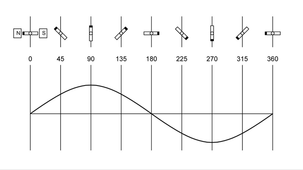
Figure A-20. Phase angle and AC generator rotation
Figures A-19 and A-20 describe a single-phase situation. In industrial and commercial AC power systems, it is common to find three phases (or in some cases six or even nine), because polyphase AC circuits tend be more efficient for power transmission and polyphase motors do not require the external starting circuit that a single-phase motor needs to produce a starting torque.
Phase plays a big role in AC circuits. An interesting thing to note about AC signals is that, when they are combined, the peaks and valleys of the waveforms add or subtract, resulting in a new waveform that is the algebraic sum of the originals. If two AC signals of exactly the same frequency but also exactly 180 degrees out of phase with respect to each other are combined, the sum is zero: they cancel out. You can hear the effect of out-of-phase signals when a pair of stereo speakers is miswired. If one is phase-reversed with respect to the other, the identical frequencies cancel, leaving only the differences. The result is often a thin, weak sound, or if the vocals are equally distributed on both the left and right channels, but the instruments are not, the vocalist might seem to fade into the background or vanish completely. This, by the way, is the basic principle behind noise-cancellation headphones.
In electronics, most of the AC will be of the single-phase type, and the main concerns in terms of phase involve phase lead or lag, phase shift, and phase angle detection. Although we have been talking about voltage phase up to this point, it is important to note that both the voltage and the current have phase, and they don’t have to be coincident in time. In other words, some circuits can induce an angular difference between the voltage phase and the current phase.
Capacitance, Inductance, Reactance, and Impedance
This section deals with the passive components that are used with AC current: capacitors and inductors. We will look briefly at reactance and impedance but won’t cover topics like phasor analysis or resonant circuits. These are very interesting topics, to be sure, but they aren’t something that I can easily wedge into a summary like this and still do them justice. Out of necessity, this appendix is an abbreviated overview, and the main intent is to introduce some basic concepts and terminology. You are encouraged to seek out more detailed sources of information if you wish to learn more about the topics presented here.
The primary focus of this section is to look at the basic behaviors of capacitors and inductors, with a focus on understanding how they interact with changing current flow. In a DC circuit, a capacitor will not pass current after it has accumulated a charge, and an inductor will behave like a low-value resistor after it is energized. It is those moments when current flow starts or stops when the behavior of these components becomes apparent, and AC is continually changing. In an AC circuit, capacitors and inductors will exhibit reactance, which is the opposition to changes in voltage or current flow. A capacitor resists changes in voltage, while an inductor resists changes in current. This is due to how each type of component stores and releases energy. When combined with a resistance, the result is impedance.
Capacitors
In its most basic form, a capacitor is a passive component that consists of two parallel plates with a small gap between them, as shown in Figure A-21. The primary operating principle of a capacitor is the storage and release of electric charge. A capacitor does not permit DC to pass, but it does have the effect of allowing AC to pass.
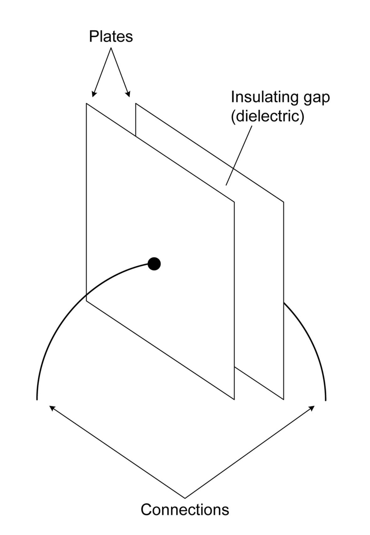
Figure A-21. A basic air-gap capacitor
As discussed in Chapter 8, most capacitors use a dialectic material (an insulator that can be polarized by an electrical charge) rather than an air gap. This allows the capacitor to be physically compact, and the characteristics of the dielectric can be tailored for specific requirements. Air can also act as a dialectric, but it can’t be tailored for a specific application.
The fundamental unit of capacitance is the farad, abbreviated as F. One farad of capacitance produces a potential difference of 1 volt when charged by 1 coulomb. As defined in “Current”, a coulomb is equal to the amount of charge, in the form of 6.2415093 × 10¹⁸ electrons, produced by a current of 1 ampere flowing for 1 second.
In reality, the farad is an impractically large unit of capacitance, so it is typically specified in smaller units using the prefixes shown in Table A-7.
|
Prefix |
Symbol |
Multiplier |
Equivalent |
|
milli |
m |
1 × 10⁻³ |
1 mF or 1,000 μF |
|
micro |
μ |
1 × 10⁻⁶ |
1 μF or 1,000 nF or 1,000,000 pF |
|
nano |
n |
1 × 10⁻⁹ |
1 nF or 1,000 pF |
|
pico |
p |
1 × 10–12 |
1 pF |
|
Table A-7. Standard value prefixes used with capacitance |
|||
Although the farad is not a practical unit of capacitance for most applications, special types of capacitors are available with values measured in farads. These are often used as short-duration batteries for memory retention power.
When a voltage is applied to a capacitor, one of the plates will become charged in one polarity, while the other plate will take on the opposite polarity. This is due to the electrostatic repulsion of like-charge particles (mentioned in Chapter 1), with the net result being that a capacitor will accumulate charges of opposite polarity on each of the plates.
When switch S1 is closed and S2 is open, charge will accumulate on the plates of the capacitor. The rate at which the charge accumulates is a function of both the capacitance of C and the value of R1 (discussed in “RC Circuits”). When switch S1 is opened and S2 is closed, the capacitor will discharge the energy it accumulated through resistor R2. The discharge rate is a function of the values of R2 and C.
Another point to take away here is that when charging, a capacitor will appear as an instantaneous short circuit to the power source. This is why resistors and large-value capacitors almost always appear together in power-supply filter circuits. It is generally not a good idea to connect a large capacitor directly to a power source, because even though the short-circuit condition is present for only a short period of time, it can lead to failure somewhere else in the circuit. For low-value capacitors, this effect is still present, but its impact on other surrounding components is negligible.
In an AC circuit, the capacitor will appear to pass the AC current as it charges and discharges with each cycle.
The ability of a capacitor to pass AC across what is effectively an open circuit prompted the 19th-century physicist James Clerk Maxwell to devise the notion of an electric displacement field. Not only did this help Maxwell visualize what was going on, but it led to the derivation of the electromagnetic wave equation that united electricity, magnetism, and optics.
Although calculations for electronics are done as if the components involved are ideal in their behavior, the reality is that there are no ideal components. The equivalent circuit for a typical capacitor, shown in Figure A-24, illustrates this.
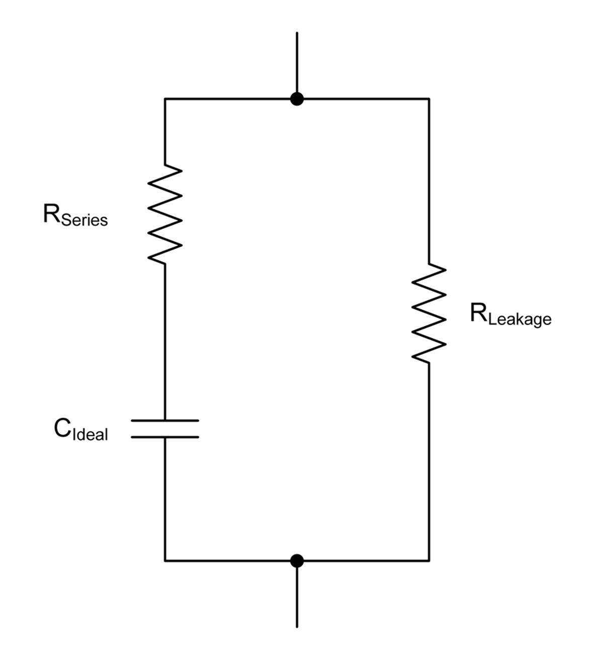
Figure A-24. Equivalent circuit for a typical capacitor
While the resistive aspects of a capacitor cannot be completely eliminated, they can be reduced. For the most part, however, the value of RSeries tends to be very low, while the value of RLeakage tends to be very high, so they can be safely ignored in most cases.
In addition to capacitive value and tolerance, capacitors are rated by working voltage, and exceeding the working voltage can result in the catastrophic failure of the part. In other words, it might explode. This becomes an important consideration when you are working with series and parallel networks of capacitors, as discussed in “Series and Parallel Capacitors”. Also, some capacitors are polarized, meaning that they have definite positive and negative connections. Electrolytic types are usually polarized, whereas ceramic types are usually nonpolarized. Incorrectly connecting a polarized capacitor will almost certainly damage it, sometimes causing a failure similar to an over-voltage condition.
In general, ceramic capacitors have working voltages into the hundreds of volts, whereas common electrolytic types range from around 10 to 100 volts. As a rule of thumb, the lower the value of the capacitor, the higher its working voltage can be.
Series and Parallel Capacitors
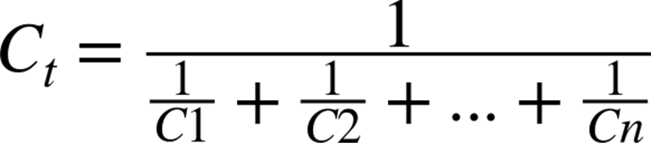
Just as with resistors, capacitors can be combined in series and parallel, although the math involved is a little different. Figure A-25 shows capacitors connected in series.
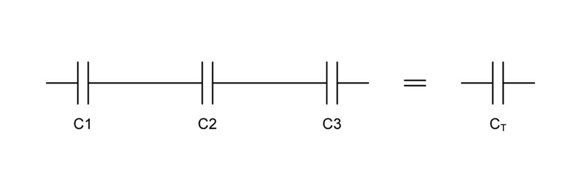
Figure A-25. Capacitors connected in series
When capacitors are connected in a series network, the total capacitance will be less than the lowest value component in the network (recall that for resistors the values are summed). The effect is equivalent to reducing the size of the plates of the capacitors in the network, thereby reducing the overall capacitance. This is given by:
Capacitors in parallel, as shown in Figure A-26, will have a total value equal to the sum of the individual components in the network. This is equivalent to increasing the overall plate area and thereby increasing the capacitance.
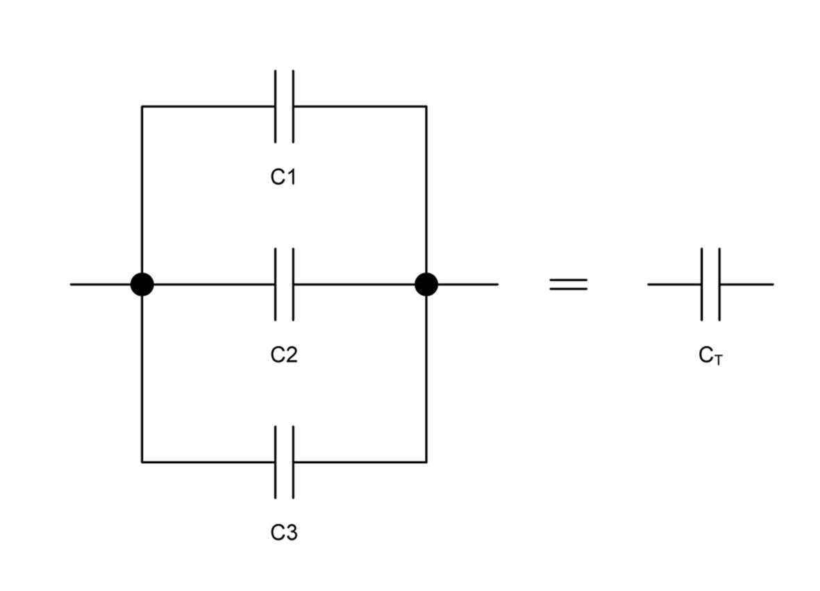
Figure A-26. Capacitors connected in parallel

Notice that capacitors in series divide, whereas resistors sum. By the same token, capacitors in parallel sum, but resistors divide.
Capacitive Coupling
To DC, a capacitor is an open circuit, but it allows AC to pass due to the fact that the AC signal will alternately charge and discharge the plates of the capacitor. Figure A-23 illustrates this when a capacitor is connected to an AC source. Figure A-27 expands on that concept with a more complete circuit.
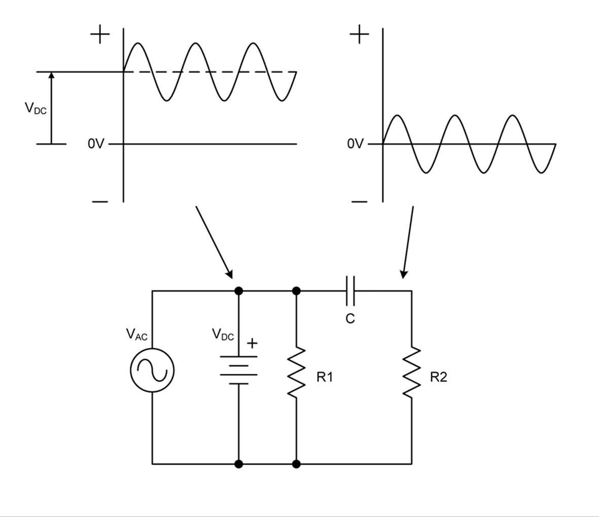
Figure A-27. DC blocking behavior of a capacitor
There are a couple of interesting things to notice in Figure A-27, where we have both an AC voltage source and a DC voltage source (a battery, for instance). The first is that AC and DC can exist simultaneously on the same wire (this is actually quite common in electronic circuits). Secondly, the AC signal will ride on top of the DC voltage, with the zero-crossing level of the AC signal at the maximum DC level. This is often referred as a DC offset or a DC bias, depending on the context.
Now notice in Figure A-27 that you can measure the composite AC-DC signal across R1, but the capacitor C will block the DC and allow only the AC to pass, so taking a measurement across R2 shows only the AC signal. We’ve neglected to consider the interaction between the resistors and the capacitor, which will affect how the circuit will respond at different frequencies. The next sections on RC circuits and reactance will cover these points.
Also note that when a DC offset or bias is present, the AC waveform no longer has true zero-crossing points when the phase is 0, 180, or 360 (0 again) degrees. In order to sense and utilize the zero-crossing points, the DC offset must be removed. A DC offset can also cause problems with bipolar circuits that are designed to swing between the V+ and V– supplies, such as op amps or audio amplifiers. In fact, a DC offset at the input of a direct-coupled audio amplifier can result in speakers with burned-out voice coils. Most speaker voice coils are not designed for continuous operation, but the coils will be continuously energized by the offset voltage. This, in turn, will cause the coils to overheat and eventually self-destruct.
For this reason, capacitive coupling is common in audio circuits, because the whole point of an audio circuit is to amplify, filter, or otherwise modify an AC signal (i.e., the audio). To deal with unwanted DC offset, capacitors are used at the inputs and between the processing or amplification stages to block unwanted DC and pass only the audio AC signal. The same technique is applied whenever a DC component in an input or output might cause a circuit to saturate, become unstable, or introduce distortion in the output.
Capacitive Phase Shift
When current flows into a capacitor, it takes some amount of time for the voltage to change. How long it will take depends on the value of the capacitor. It’s akin to filling a tub with sand. The sand might be coming in at a fixed rate, but the tub will not fill instantly. At some point, the tub will be full of sand and the filling can stop. Assuming that the sand is supplied at the same fixed rate, a larger tub will take longer to fill. For any given amount of available current, a small-value capacitor will reach its maximum charge (i.e., it will be full) sooner than a capacitor with a large plate area. In both cases, when the charge is equal to the maximum supply potential, the current flow stops.
The main point here is that the current has to flow first, and the charge then catches up to it. The result is that the current leads the voltage, as shown in Figure A-28. Notice the 90-degree difference in the phases; this will come up again later in the discussion of reactance and impedance.
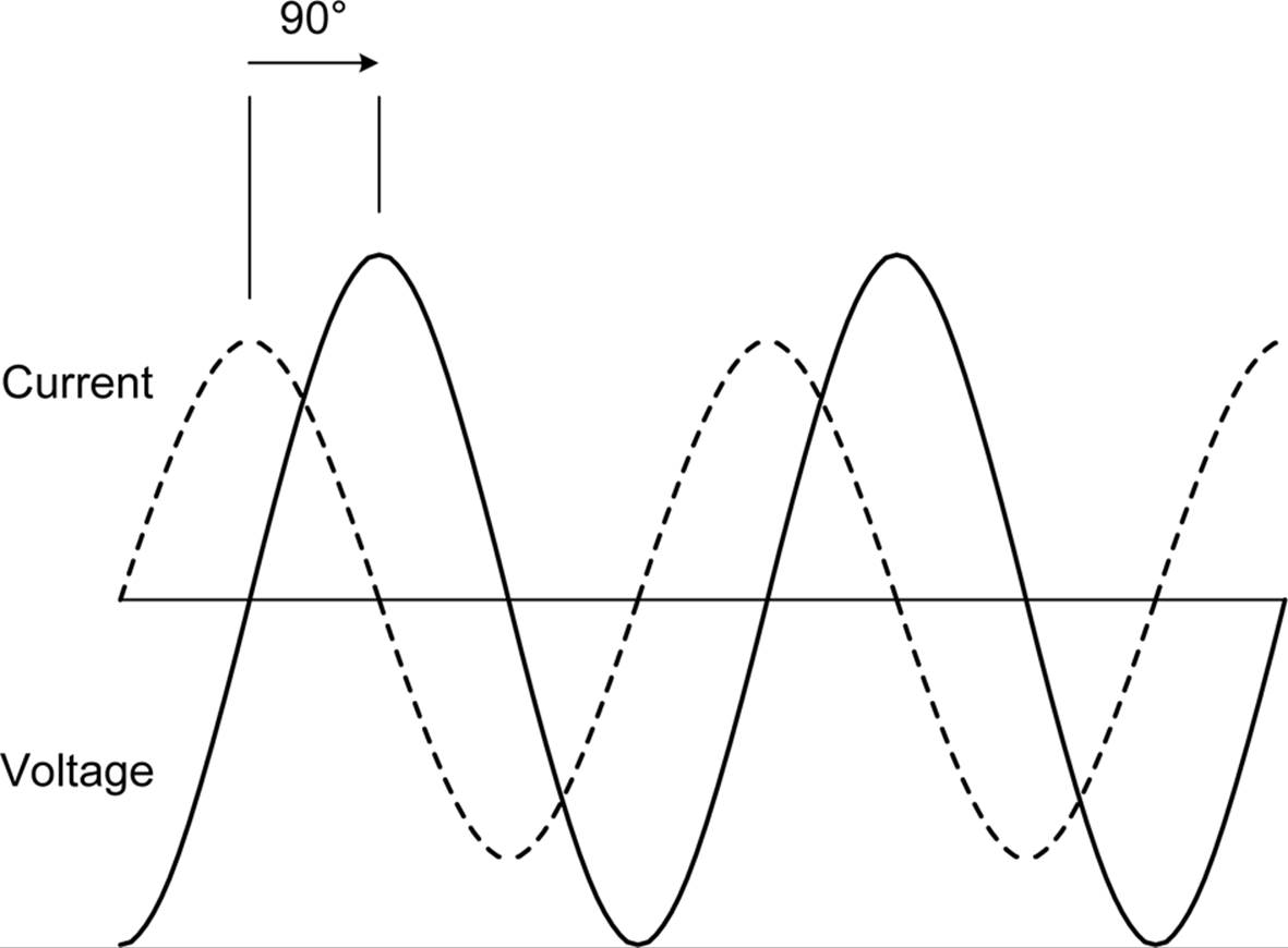
Figure A-28. Capacitive phase shift: current leads voltage
Conversely, when the AC voltage starts to head back to zero, the current again starts to flow, only now in the opposite direction. The current again leads the voltage and reaches its maximum negative value 90 degrees ahead of the voltage.
RC Circuits
As you’ve already seen, when current is applied to a capacitor, it will initially appear as a short, and current will continue to flow until the capacitor is charged. Placing a resistor in series with the capacitor, as shown in Figure A-29, limits the amount of current that can flow into it and consequently increases the time required to charge the capacitor.
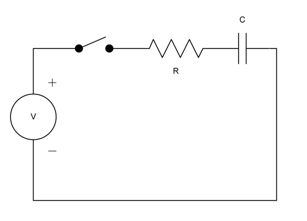
Figure A-29. Simple RC circuit
When the switch in Figure A-29 is closed, the capacitor will begin to charge. The amount of available current is limited by the resistor, R, so it will take longer for the capacitor to reach Vmax than if R were not present, as shown in Figure A-30. The current starts at the maximum possible level (Imax) available through the resistor.
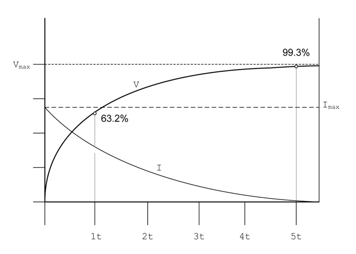
Figure A-30. R-C charge time
The period between the start of current flow and when the charge is close to 100% is divided into five intervals. The first interval, 1T, is at about 63.2% of the maximum charge on the capacitor. Each increase of 63.2% relative to the previous interval is defined by:
![]()
R is in ohms, and C is in farads. This is called the RC time constant. T is also known as tau and is expressed in units of seconds. It is derived from the mathematical constant e, and some more math that defines the voltage to charge the capacitor versus time, as discussed regarding the universal timing equation in “RC Applications”. Imax is determined by the value of R and is the current into the capacitor when it initially appears as a short circuit. As the capacitor charges, the current will decrease until it reaches a value close to zero.
After each time interval, the capacitor will have charged another 63.2% from the previous tau value, as shown in Table A-8. In other words, with a supply of 1V, the capacitor will have 0.632V after 1 tau, 0.865V after 2 tau, and so on until at the fifth tau it is at 99.3% capacity with .993V.
|
Tau |
Charge % |
|
1 |
63.2 |
|
2 |
86.5 |
|
3 |
95.0 |
|
4 |
98.2 |
|
5 |
99.3 |
|
Table A-8. RC tau time constant capacitor charging |
|
Looking again at Table A-8, you can see that the first tau point is achieved fairly rapidly, but after that, the charge gain for each successive tau interval slows down, because it’s an exponential function. At 2 tau (2RC), the capacitor will have gained only an additional 23.3%, and between 2 tau and 3 tau, it will have gained only 8.5%.
Note that the 1T, 2T, etc., notation does not imply one second, two seconds, and so on. It is simply the point at which a 63.2% relative increase in charge occurs. The value of tau itself is time in seconds, and it can be anything.
RC Applications
The RC time constant is one of the most widely used concepts in electronics. For example, an RC circuit can be used to delay an action. Consider Figure A-31, which shows an RC circuit providing input to a 7408 TTL logic gate.
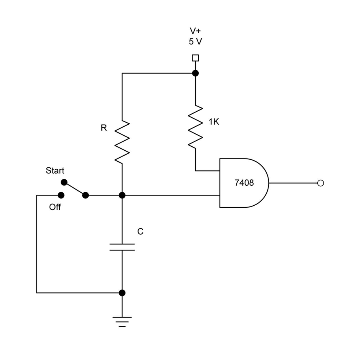
Figure A-31. Simple RC delay circuit
The 1K resistor keeps one input of the gate pulled up, which prevents any false triggers from stray gate voltage or noise. When the switch is in the Off position, the junction of R and C is pulled to ground. When it is in the Start position, C can begin to charge through R. Since this is connected to a 7408 TTL gate, the key here is to determine the values for R and C such that it will reach the threshold of the gate in the desired amount of time. Let’s pick 1 second as the target time.
We know that a TTL type gate will detect a high level input at about 2V, so when the voltage at the junction of R and C reaches 2V, the logic gate will detect a high input and its output will become high. The problem here is that with 5V supply, the 2V we want is less than the first tau of 63.2% by 1.2 volts, since 2V is actually 40% of 5V. Figure A-32 shows the situation.
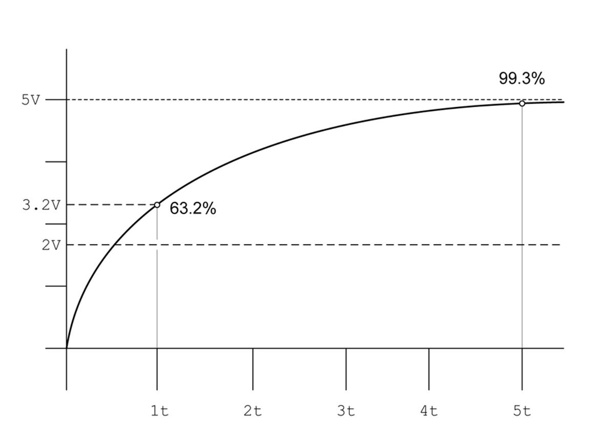
Figure A-32. RC time delay tau charge rate
We’ll use the universal time constant equation, which allows us to determine the voltage across C at some point in time relative to a particular value for tau. Looking at Figure A-32, you can see that what we want is close to being half of 1 tau, so we’ll pick tau of 2 seconds as our starting point, which should put the threshold level near the 1 second mark.
For the voltage across C at some time T, we can use a new equation, the universal time constant formula, which looks like this:
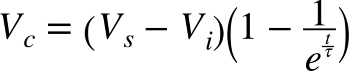
This equation describes the charging of a capacitor through a resistor at some specific point in time as an exponential function. Remember that RC simply determines the time between tau intervals, so to get the voltage at the in-between points, we need to compute the voltage along the charge curve at a particular point in time.
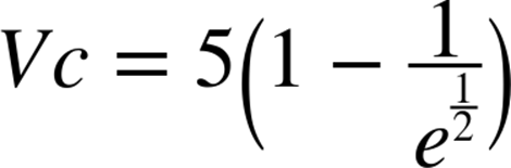
Vc is the voltage across C; Vs is the final voltage minus the starting voltage, Vi. In this case, it will be (5 – 0), or just the supply voltage of 5V. The time t is 1 second, and the value of e, Euler’s constant, is approximately 2.7182818. The value of tau, as stated earlier, is 2. To determine the value of Vc after 1 second, plug in the values and turn the crank:
This returns 1.967V for Vc after 1 second, which is probably close enough, given that common components have between 5 and 20% tolerance ratings. In reality, if the circuit needs a more precise time, it should probably be using a 555 timer IC (covered in Chapter 9) or a digital timer of some sort.
We have our tau of 2, so let’s pick an R and see what kind of C we would need. Do this by solving the RC time constant equation for C, using 200 k for R:
This gives a value for C of 0.00001 farads, which is 10 μF. This would be an electrolytic component of some type. With an R of 200 k, you can expect to see a maximum of 25 μA into C with a 5V supply, and the value of R is just a number that was chosen as a starting point because I know that the larger R is, the smaller C will be for a given tau. We could also have picked a value for C and then solved for R.
In addition to serving as a time delay, the charging time of an RC circuit can shift the phase of an AC signal, an effect that is dependent on the impedance of the RC circuit, which is itself a product of the resistance and capacitance (“Impedance and Reactance” discusses impedance). This behavior can be used for AC power control applications. Thyristor devices, such as silicon-controlled rectifiers (SCRs) and TRIACs (described in Chapter 9), are designed for use with AC power circuits. They are triggered into conduction at a particular voltage phase angle and continue to conduct until the phase returns to zero (or very close to it). This is how a standard household light dimmer works, as shown in Figure A-33.
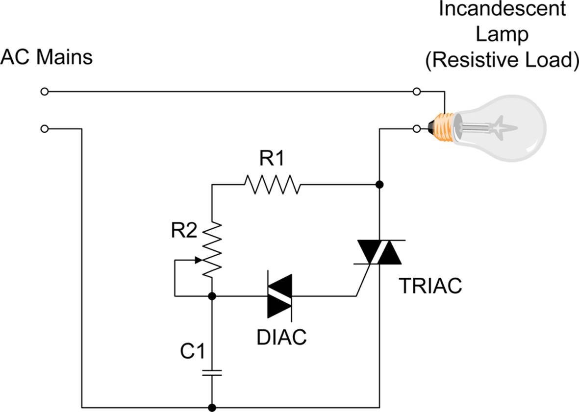
Figure A-33. AC lamp dimmer circuit
The dimmer works by enabling the TRIAC only for some portion of the AC waveform at a particular phase angle. The DIAC device acts as a trigger for the TRIAC, and it is controlled by the RC time constant of R1, R2, and C1, which form a phase delay network. By varying R2, the 1T point is shifted and the TRIAC is triggered at the phase angle corresponding to the delay. The TRIAC will remain in the on (conductive) state until the waveform returns to zero. The net result is that the circuit is selecting some portion of the AC phase at which the TRIAC becomes active.Figure A-34 shows how this works.
When the phase delay is long, the voltage across C1 takes longer to reach the trigger level of the DIAC, less of the AC waveform is passed by the TRIAC, and the lamp will be dim. As the value of R2 is decreased, the phase delay is reduced, C1 will reach the trigger level more quickly in the cycle, and the TRIAC will start to conduct sooner so that more of the AC waveform is passed on to the load.
Inductors
When current flows in a conductor, it induces a magnetic field around the conductor; and when a conductor moves through a magnetic field, a current is induced in the conductor. The interaction between electric current and magnetism has been observed in one form or another for over 400 years, but it wasn’t formally spelled out until James Clerk Maxwell, building on the work of Michael Faraday and others, described the relationship between electric charge, magnetic poles, electric current, and magnetic fields in his Treatise on Electricity and Magnetism in 1873.
In its simplest form, an inductor is just a conductor, like a section of wire. As current flows through the wire, a magnetic field will form around it, as shown in Figure A-35. The strength of the field is related to the amount of the current flowing through the conductor. If the wire is formed into a coil, as shown in Figure A-35, the intensity of the magnetic field is increased proportionally to the number of turns in the coil.
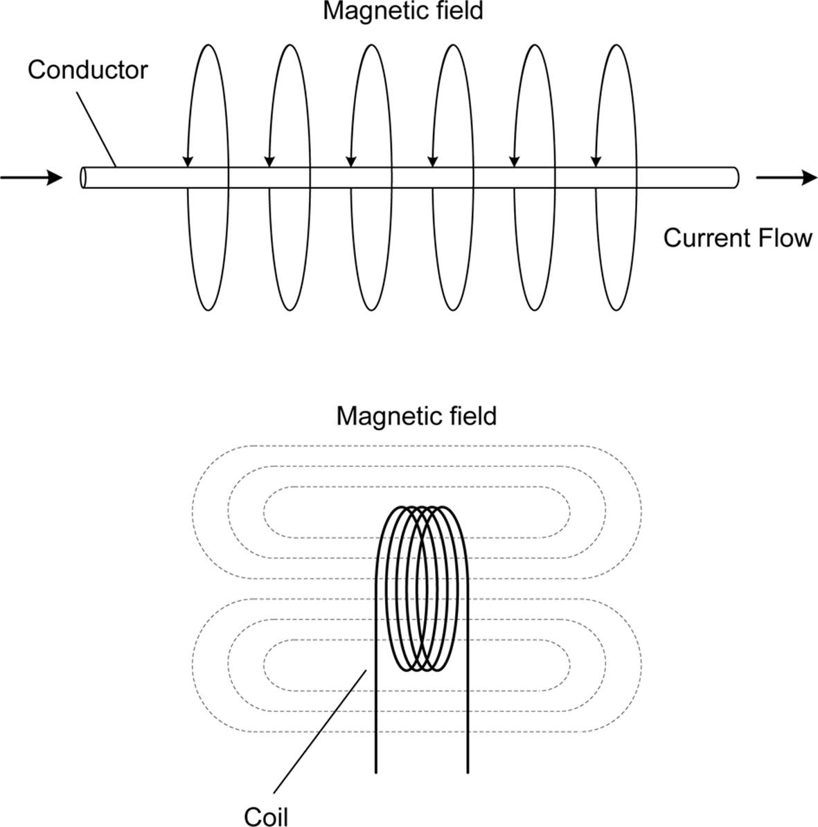
Figure A-35. Electromagnetic fields around conductors
Strictly speaking, an electromagnet, like the huge things used to pick up and move scrap metal in a scrapyard, is not an inductor. Once the current starts to flow, the magnetic field forms and will remain constant until the current flow ceases.
Inductance is the result of a changing magnetic field. During the times when the current is starting or stopping, an inductor is creating a changing magnetic field around itself, and this field interacts with the wire in the inductor as it expands and shrinks.
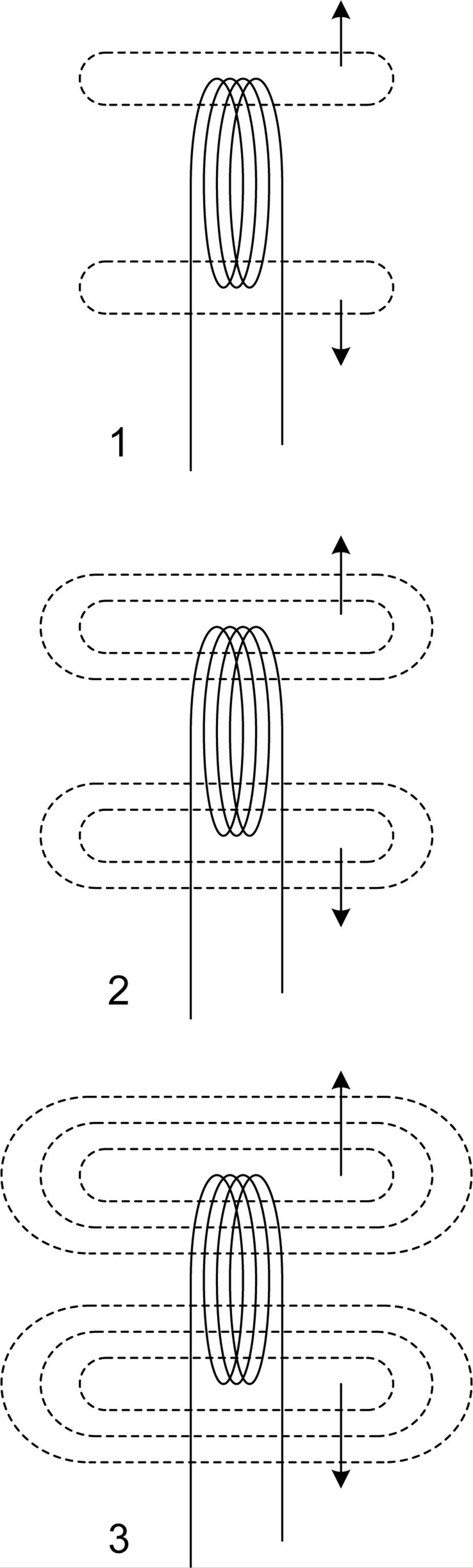
Figure A-36. Moving magnetic field in an inductor
Since a magnetic field will induce current flow in a conductor as the conductor moves through the field, the same effect holds if the magnetic field moves through the conductor. In Figure A-36, the EM field grows in steps 1 through 3, and when the current flow through the coil returns to zero, the steps are reversed as 3 through 1. The current induced by the EM field will want to flow in the opposite direction as the current that is creating the EM field. In other words, an inductor will impede a change in current flow, as discussed in “Impedance and Reactance”.
Whereas a capacitor impedes (blocks) DC, an inductor impedes AC. But in a DC circuit, an inductor reacts only when the current flow is changing from off to on, or on to off. When the current flow in a DC circuit is steady, the inductor might present a slight resistance, but nothing else.
The unit of measurement of inductance is the henry. The simplistic definition of a henry can be stated as a rate of change of current of 1 ampere per second with a resulting electromotive force of 1 volt. The full definition is beyond the scope of this book, and it involves magnetic field strength and other things. If you’re curious, refer to one of the texts listed in Appendix C. For our purpose here, the simple definition will suffice.
Like the farad, a henry is a large unit and not practical to work with, so most of the inductors you will encounter in electronics are rated in the millihenry (mh) range. As the value of an inductor increases, so does its effective impedance. The value of an inductor is a function of the number of turns of wire involved (one, in the case of a single wire), and what type of core material is used. Air does not contribute to inductance, but an iron core, for example, does.
Series and Parallel Inductors
For inductors connected in series, as shown in Figure A-37, the current through all the components of the network will be the same, but the voltage drop across each inductor might be different.
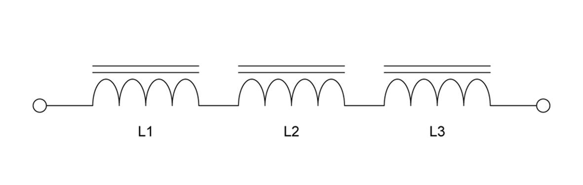
Figure A-37. Inductors in series
The total equivalent inductance is simply the sum of the individual inductive values:
Inductors in parallel have the same voltage potential across each component, but the current, depending on the inductance and the frequency of the signal across them, will vary. Figure A-38 shows a parallel inductor network with three components.
The equivalent inductance is calculated through the equation:
These simple equations work only when there is no inductive coupling between the components.
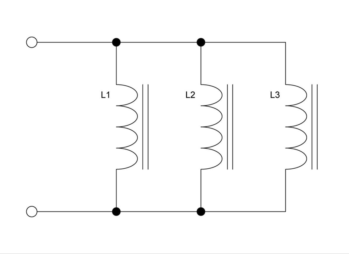
Figure A-38. Inductors in parallel
Inductive Phase Shift
When an inductor is energized, or when it is supplied with AC, the current flow is impeded but the voltage is not. The result is that the voltage leads the current, as shown in Figure A-39.
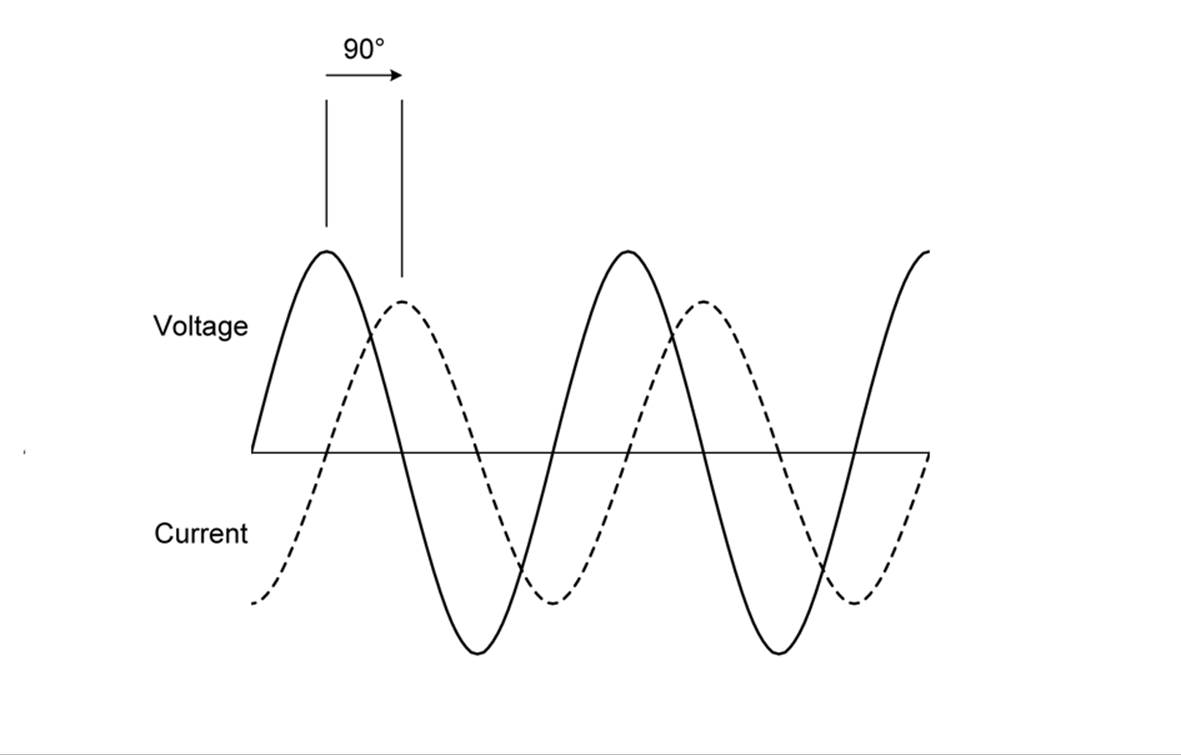
Figure A-39. Inductive phase shift: voltage leads current
To help understand why this is, recall that when current flows through an inductor, a magnetic field will be created (as shown in Figure A-36). As the magnetic field expands, it intersects the wires in the coil of the inductor. This, in turn, creates a reverse current flow (sometimes called back EMF) that will oppose the incoming current. The voltage remains unaffected, for the most part. When the voltage reaches a steady state (which is at the minimum or maximum extents for the waveform of an AC signal), the current flow momentarily goes to zero and the coil’s field ceases to expand (or contract), and no more reverse current flow is generated.
In the case of AC, when the voltage begins to drop in the second half of the waveform, the inductor again creates a reverse current flow as the magnetic field collapses and the field intersects the wires in the inductor’s coil—only now the field is moving the opposite direction.
Inductive Kick-Back
The same effect that causes an inductor to induce lagging current when current starts to flow or with an AC signal is also responsible for the sharp voltage spike that is seen when a solenoid-type inductor (i.e., a relay) is de-energized. Consider the simple circuit shown in Figure A-40.
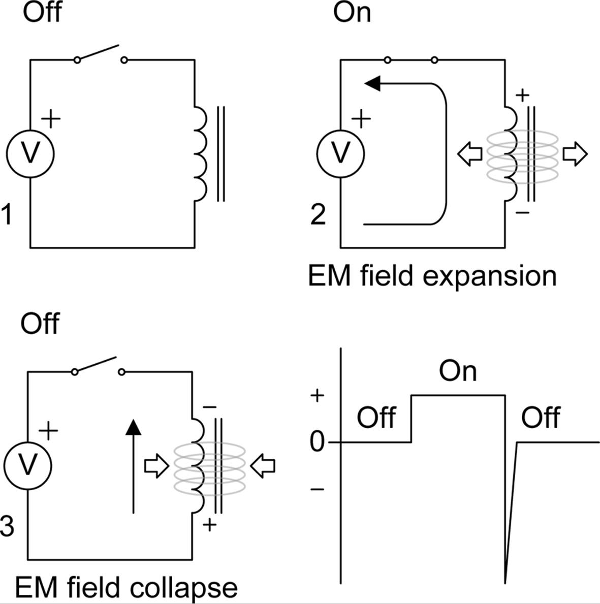
Figure A-40. Voltage spike created when an inductor is de-energized
The graph on the right side of Figure A-40 shows what you could expect to see if you monitored the voltage drop across the inductor with an oscilloscope. The spike that appears when current ceases to flow in the inductor arises as the magnetic field in the inductor collapses. This occurs very quickly, and the spike is often very large (sometimes many hundreds of volts). As the field collapses, the effective direction of current flow will remain the same, but the voltage across the coil will be inverted, because it is now acting as a current source. Also, notice the the current flow inFigure A-40 is shown as electron flow, not conventional current flow.
The kick-back voltage from an inductor can create arcing across switch contacts, and it can easily destroy solid-state devices. Since in a DC circuit the spike will always be the opposite polarity of the voltage that energized the coil, a diode can be used to return the spike back to the coil and harmlessly dissipate its energy, as shown in Figure A-41.
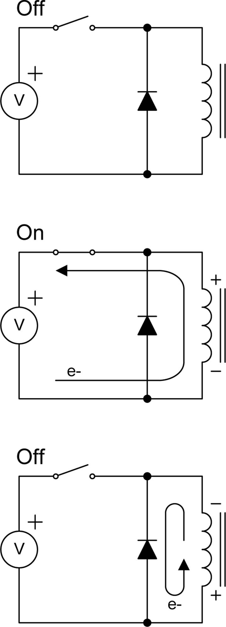
Figure A-41. Using a diode to snub the reverse spike from an inductor
When an active component, such as an IC or a transistor, is used to drive a relay, the kick-back from the coil in the relay can destroy the solid-state part by suddenly presenting a voltage that is far beyond what the device might be rated for, as shown in Figure A-42.
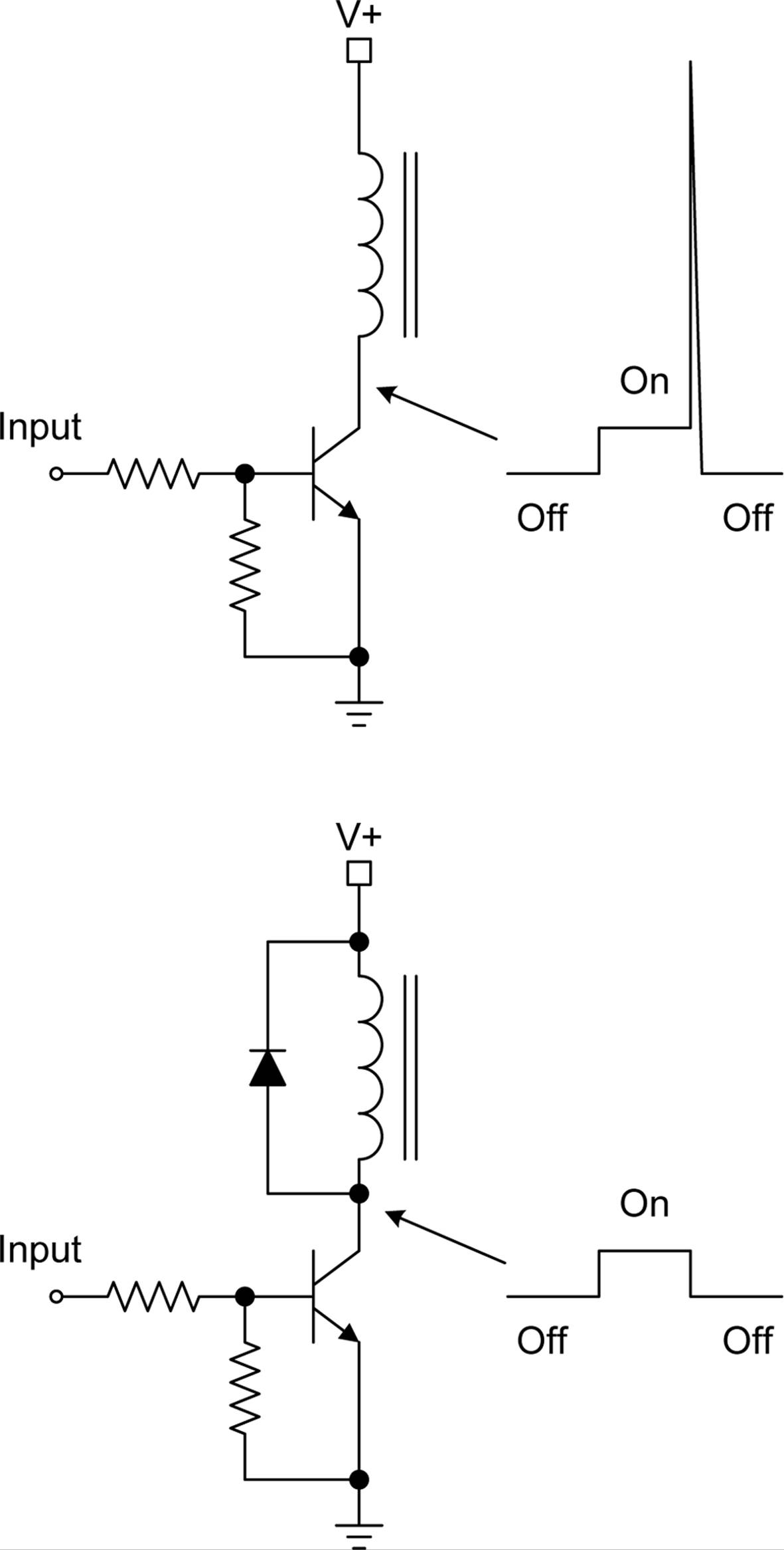
Figure A-42. Protecting a transistor with a kick-back snubber diode
Notice that, from the perspective of the transistor, the spike from the relay appears to be positive. This is because, when the field collapses, the coil becomes a momentary current source and the current flow is the same direction as when it was energized. The end of the relay coil connected to the transistor becomes positive, and the now negative end of the relay coil is connected to the positive power supply. It is equivalent to inserting a battery in place of the relay. With a diode installed across the coil of the relay, it effectively short-circuits the reverse voltage current flow from the coil due to field collapse, thereby saving the transistor from destruction.
Impedance and Reactance
Capacitors resist changes in voltage, and inductors resist changes in current. In AC circuits, this opposition is typically called impedance, and the reactance of the component is a fundamental part of the impedance. This section provides a quick summary of reactance and impedance, but working through the math in detail is beyond the scope of this book. Refer to one of the texts on electronics in Appendix C for the low-level details. The ARRL Handbook and William Orr’s Radio Handbook, for example, both cover these topics in some detail, with lots of practical applications for tuned circuits and antennas.
Reactance
The reactance is the opposition of a circuit element to changes in voltage or current, and it is a result of the circuit element’s capacitance or inductance. So, although they are typically classified as passive components, capacitors and inductors also fall into the category of reactive components.
As shown earlier in the sections on capacitors and inductors, reactive components store and release energy. Capacitors store voltage in the form of an electric field, while inductors store current in the form of a magnetic field. Because work is required to store the energy in the components, they appear as loads when the current is changing. In an AC circuit, the current is constantly changing, so the load is persistent. This, in essence, is reactance. It is similar in some respects to resistance, but it is not the same thing.
It is reactance that gives rise to impedance. In an AC circuit, reactance is frequency dependent. Reactive components don’t typically respond to DC (except for the appearance and cessation of current flow). An inductor, for example, will appear as a simple resistance to DC. A capacitor will appear as an open circuit. An ideal resistor, on the other hand, does not react to a change in current flow. It just presents a resistance regardless of whether or not the current flow is DC or AC.
The magnitude of the reactance of a capacitor is inversely proportional to frequency. In other words, the higher the frequency, the lower the reactance of the capacitor to the AC signal. The magnitude of the reactance of an inductor is also proportional to frequency, with the reactance increasing as the frequency increases. It is the opposite of a capacitor. Figure A-43 shows these relationships graphically. Note that reactance is denoted with the symbols XL and XC and specified in units of ohms.
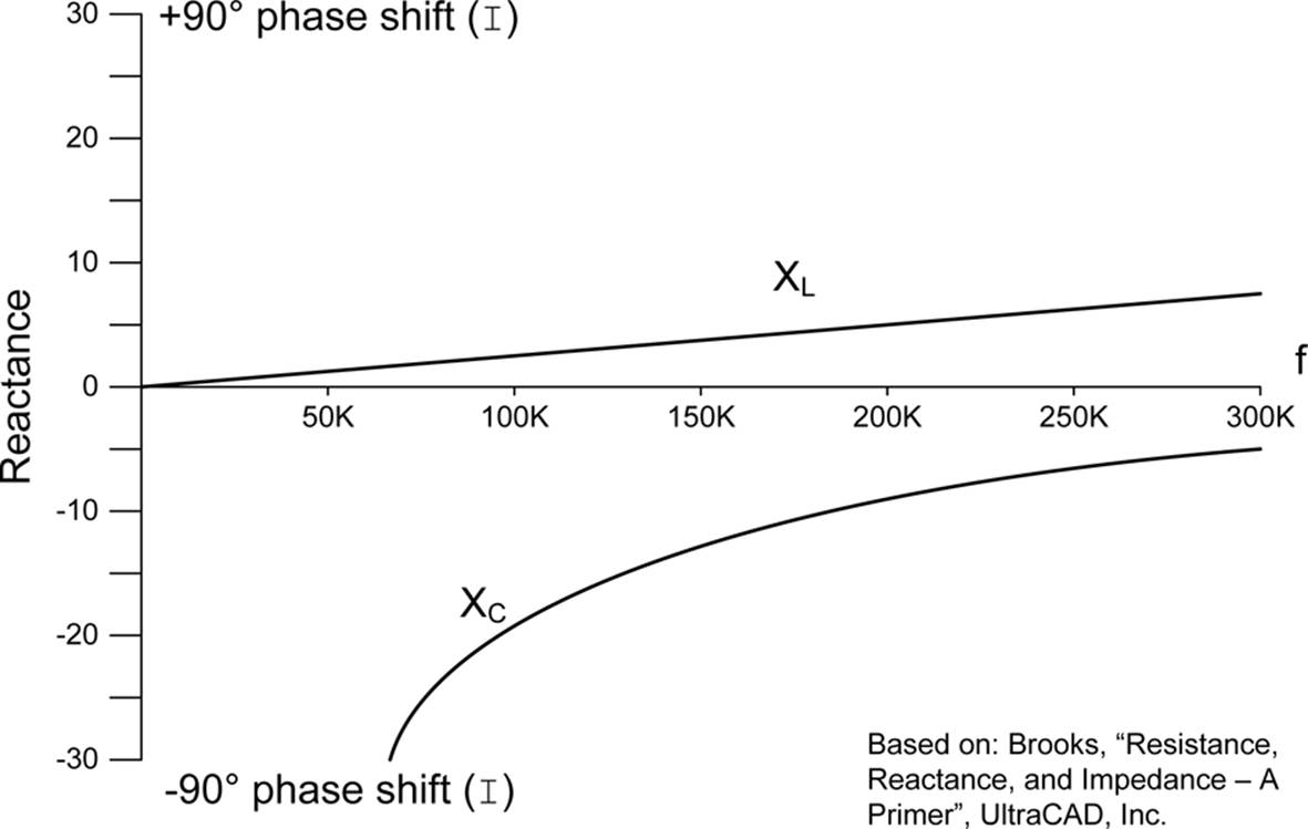
Figure A-43. Inductive and capacitive reactance versus frequency
These types of plots would usually employ a logarithmic scale to make them easier to comprehend, but it’s informative to see them in their raw form.
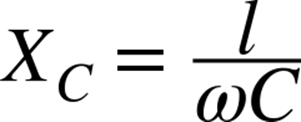
The math necessary to find the reactance of a capacitor or inductor is straightforward. For capacitive reactance, you can do the following:
And for inductive reactance:

Note that C is in farads, L is in henries, and both XC and XL are in ohms. Also recall that:
Impedance
Impedance is the sum of resistance and reactance. Ideal capacitors and inductors have only reactance, and they will cause a shift in the phase of the current relative to voltage. A resistor does have an associated phase shift, because it is not a reactive component.
In a purely reactive component, the phase shift is always 90 degrees. A capacitor causes the current phase to lag (–90 degrees) and an inductor causes the current phase to lead (+90 degrees). Impedance is what happens when a resistance enters the picture and modifies the current flow, although the term impedance is also used when we are discussing interaction of capacitors and inductors with an AC signal.
As shown earlier with RC circuits, a resistance can change the rate of charge on a capacitor and in the process alter the voltage-current phase relationship to some angle other than 90 degrees. This is the key principle behind the TRIAC circuit presented earlier.
The letter Z is used to denote impedance, and the relationship is given as:
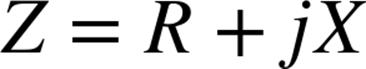
Note that j is the square root of –1, an imaginary number. Conventional mathematics uses the letter i; but in engineering, the letter j is used to avoid confusion with I, the letter used for current.
One of the main applications of the concept of impedance arises when we consider a circuit as a whole, with all of its internal resistances and reactances. Recall that the unit of measure for reactance is ohms and that, for a particular frequency, a capacitor or inductor will have a specific reactance. It follows then that we could apply Thévenin’s theorem to a circuit composed of resistances and reactances, and this is indeed the case. From this we can determine the impedance of the equivalent circuit. In the interests of keeping this appendix short and concise, we won’t work through the math, but there are excellent examples in the text listed in Appendix C.
Passive Filtering
A combination of resistance, capacitance, and inductance can and often is used for passive filtering. Passive filters, as the name implies, have no signal amplifying elements such as transistors or op amps. Consequently, a passive filter has no signal gain. This means that the output level of a passive filter is always less than the input.
For low frequencies (from 0 to around 100 kHz), passive filters are generally constructed with simple RC networks, while higher frequency filters (above 100 kHz, or RF-type signals) are usually made from a combination of RLC components. This section looks at simple low-pass and high-pass RC filters as a way of showing how the concepts of reactance and impedance for RC circuits can be applied in practical ways. Although we won’t get into LC and RLC filters, the concepts for these also follow from the material already presented, and in-depth discussions can be found in the texts listed in Appendix C.
Recall that a capacitor will pass high frequencies but block low frequencies (including DC). This implies that a capacitor in parallel across an AC signal will shunt high frequencies to ground, and a capacitor in series with the signal will pass high frequencies but block low frequencies. The inclusion of a resistor into the network allows the behavior to be adjusted for a specific range of frequencies.
Figure A-44 shows a simple RC low-pass filter. In this arrangement, the capacitor, C, will shunt high-frequency signals to ground, but allow low-frequency signals to pass through from input to output.
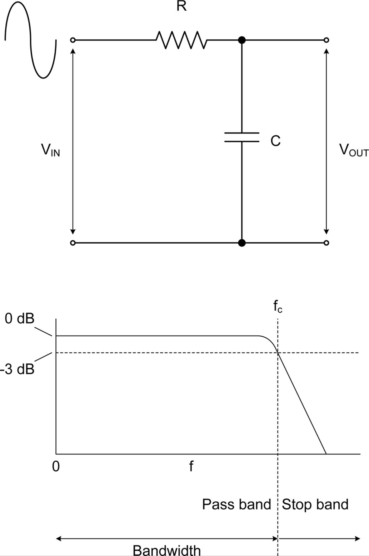
Figure A-44. Low-pass RC filter
The cutoff frequency, fc, is defined to be the point where the output of the filter drops by –3 dB. Decibels are commonly used with AC signals, and it is a logarithmic scale. Decibels are used to express the ratio between two values, and in the case of Figure A-44, it refers to the decrease in the output of the filter at the cut-off frequency. The cut-off frequency is the point where the response begins the drop towards zero, and it is at this point where the capacitive reactance and the resistance are equal, and the output is 70.7% of the input.
The rate at which the filter will attenuate the signal is called the roll-off rate and is expressed in dB per decade, or dB per octave. A decade is a 10-fold change in frequency, and an octave is a 2-fold change in frequency. A passive low-pass or high-pass RC filter will typically exhibit a 20 dB/decade roll-off.
The cut-off frequency for a low-pass filter is calculated as follows:
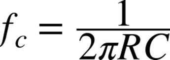
Assume you wanted to filter an input to an A/D converter (an ADC) to reject any noise that might be present. If the signal you want to sample will always be less than 100 Hz, you can rearrange the equation, pick a value for R, and solve for C at 100 Hz. Let’s pick a value for R, say 10,000 ohms, and shuffle the preceding equation to solve for C:
Remember that C is in farads, so the capacitor needed is 0.159 μF. A 0.15 μF part is close enough, and it is a standard value. Since there is an inverse relationship between the value of R and the value of C, picking something like 10 k ohms for R is a reasonable place to start.
A high-pass filter takes advantage of the reactance of a capacitor to block signals below the cut-off frequency. Figure A-45 shows a high-pass RC filter. The equation for a passive high-pass filter is the same as for the low-pass filter.
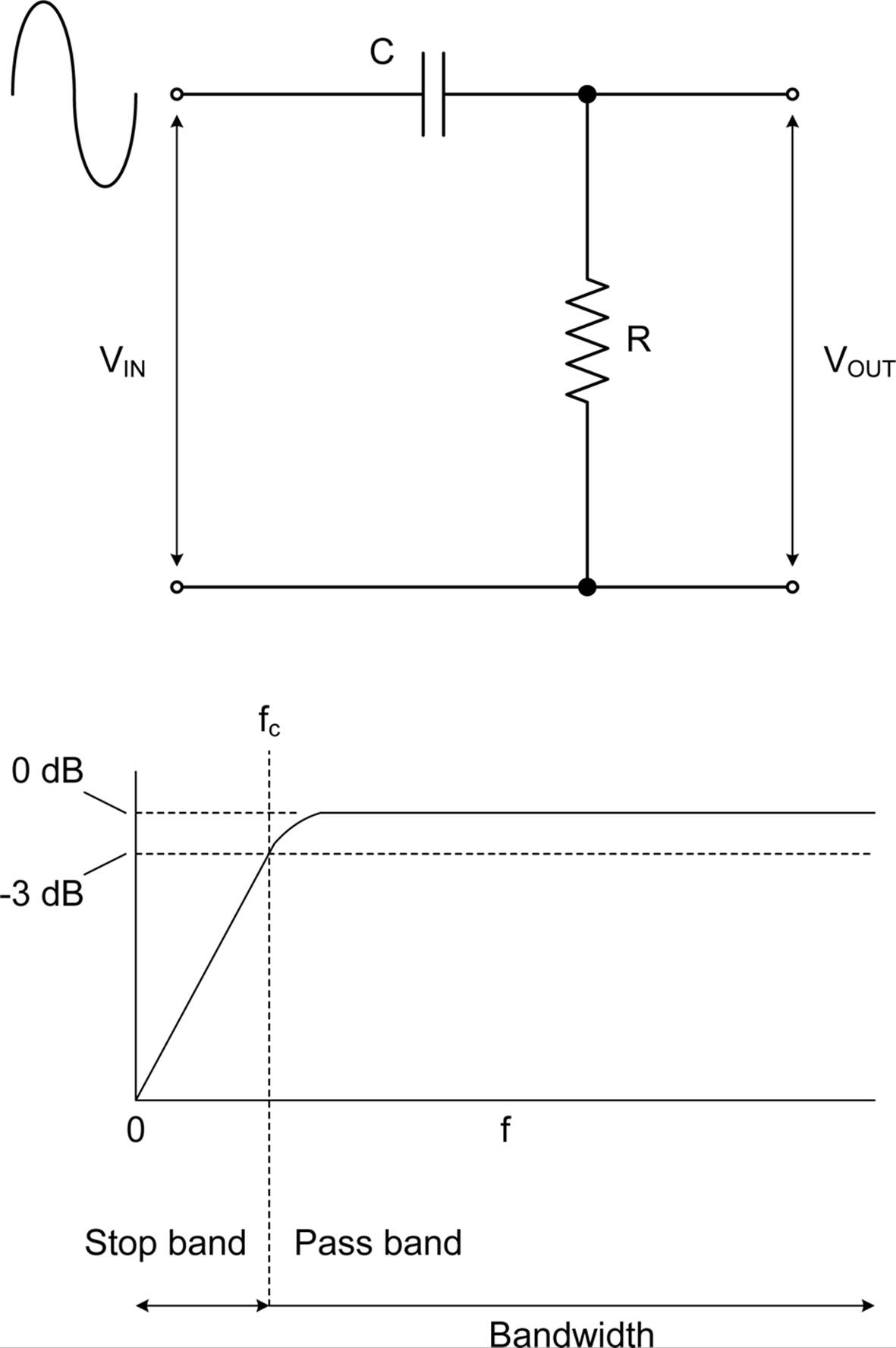
Figure A-45. High-pass RC filter
Both of the filters shown here are called single-pole filters, meaning there is only one network of R and C. Multi-pole filters use two of more RC filters to increase the roll-off rate of the filter response, but at the cost of increased signal attenuation and filter accuracy.
Solid-State Concepts
This section presents a high-level overview of solid-state devices. The brevity is out of necessity, since there is not enough room to cover the field with any significant level of detail. Ideally, you should be able to get a handle on the basic concepts and have a good idea where to turn next for more information.
As discussed in Chapter 1, copper, silver, and gold are good conductors, and things like plastics, ceramics, and sulfur are good insulators. Semiconductor materials such as silicon (Si), germanium (Ge), or gallium arsenide (GaAs) lie between insulators and conductors. In terms of conductivity, we can say that they are only partially conductive, hence the name semiconductor. But a semiconductor is not a resistor, because a semiconductor will exhibit nonlinear behavior under certain conditions, whereas a resistor will always behave in a linear fashion in response to current.
Silicon-based semiconductor components are fabricated on thin sheets cut from a silicon crystal grown in a special oven. Each circular sheet, called a wafer, can contain hundreds of individual parts. After the parts are created on the surface of the wafer, they are tested using automated machinery. Those parts that fail testing are tagged by their location on the wafer and will be discarded later when a diamond saw cuts the wafer up into individual chips. The chips are then mounted in a package of some type: small diodes in a package with two lead, transistors in a three-terminal package, and ICs in packages with anywhere from 8 to 144 leads or contact points, or more.
The manufacture of semiconductors is complex and utilizes highly specialized and expensive automated equipment. However, many millions of solid-state devices are produced each year, and the economy of scale, coupled with high levels of automation, allow prices to remain astonishingly low. The advances in technology have continued unabated over the years, with each new generation of semiconductor components being smaller, cheaper, and denser than the preceding generation. As Gordon Moore, Chairman Emeritus of Intel, was reported to have said in 1998, “If the automobile industry advanced as rapidly as the semiconductor industry, a Rolls-Royce would get half a million miles per gallon, and it would be cheaper to throw it away than to park it.”
The P-N Junction
Modern solid-state devices are based on the physics of semiconductor materials that have been altered (or doped) to enhance their ability to conduct current in a particular manner. The doping takes the form of an infusion of so-called impurities (impure in the sense that they are not part of the original semiconductor). These atoms are the donors and acceptors of electrons that allow current to flow across the junction.
The basic arrangement of semiconductor material with different characteristics is called a P-N junction, and this is the basis for the ubiquitous diode. Adding a second junction results in a bipolar junction transistor (a BJT), and other arrangements are used to create field-effect transistors (FETs), SCRs, TRIACs, Zener diodes, LEDs, and integrated circuits. Figure A-46 shows a simplified diagram of a P-N junction.
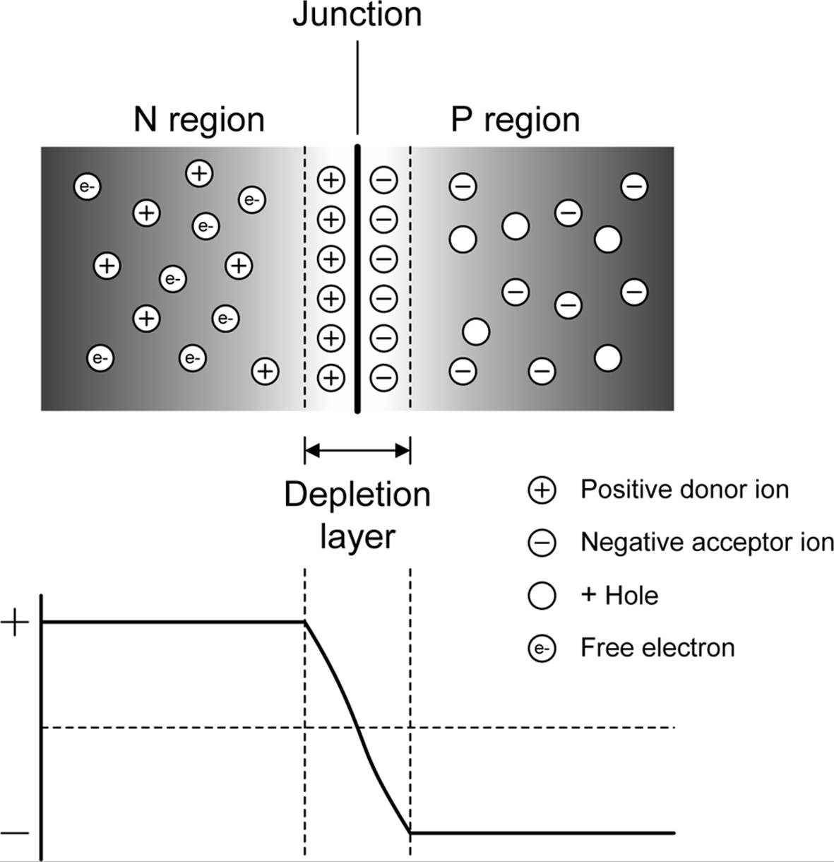
Figure A-46. Simplified P-N junction
Shortly after the junction is formed, some of the free electrons from the N side move to the P side. At the same time, positive holes (where an electron is missing) move through the semiconductor from the P side to the N side. When no more charges can move (or diffuse), the result is a region at the junction that is depleted of any free charge carriers, called the depletion layer, and a charge gradient appears across the junction.
Diodes and Rectifiers
The interface between P- and N-type semiconductor material moves charge more easily in one direction than the other so that negative charges in the form of electrons can flow easily from the N to the P side of the junction, but not in the opposite direction. This is the basis for solid-state diodes. Figure A-47 shows how the symbol for a diode correlates with the P and N semiconductor material in the component. The semiconductor material is usually silicon crystal, but special-purpose diodes can employ germanium or gallium arsenide.
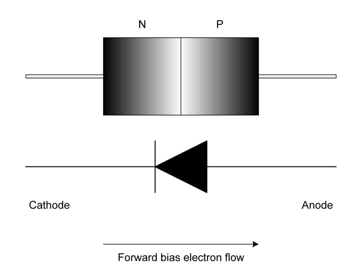
Figure A-47. P-N junction diode
Referring back to Figure A-46, you can see that the N-type material has a surplus of electrons (e–), also called charge carriers, while the P-type material has a surplus of positive charge carriers called holes. Note that there no charge carriers in the depletion layer.
For a simple P-N junction device, when a voltage is placed across a diode with the opposite polarity as the inherent potential across the depletion layer, the process of charge migration that initially occurred when the junction was formed will begin again, and as a result, current will flow across the junction. A P-N junction in this state is said to be forward biased. When an external voltage is applied to the junction with the same polarity as the junction’s potential gradient, the depletion layer will simply continue to act as an insulator, blocking the movement of electrons and holes and thereby preventing current flow. This is called reverse bias.
The junction potential for silicon diode is approximately 0.7V. For Germanium diodes, it is around 0.3V, and Schottky diodes are about 0.2V. In order for a diode to be forward biased, the external voltage must exceed the junction potential. This is sometimes referred to as the threshold voltage of a diode. It conducts when the external voltage is greater than the threshold, but it does not conduct when it is less than the threshold level.
A common way to visualize what is going on in the P-N junction of a diode is called an I-V curve, as shown in Figure A-48. As you can see, the diode will not conduct until the voltage across it reaches the junction threshold, after which it conducts in a logarithmic fashion.
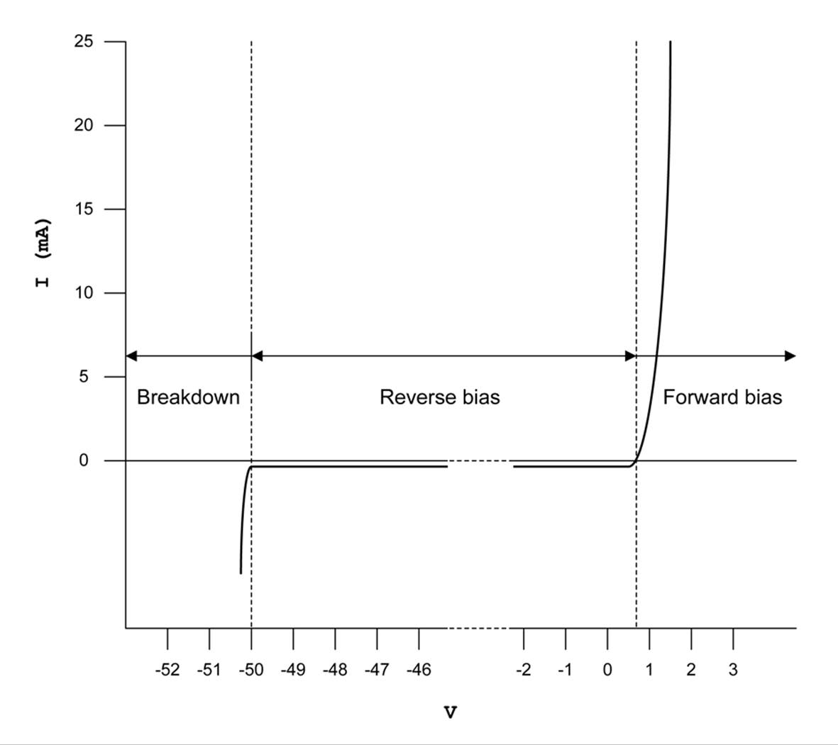
Figure A-48. I-V curve for a common silicon diode
One of the parameters used with diodes (and any solid-state part, for that matter) is the peak-inverse-voltage (PIV), which is the maximum voltage that the part can tolerate in the reverse bias state before the P-N junction breaks down. The graph in Figure A-48 shows a small amount of current flowing while the device is reverse biased. This is called the reverse saturation current, and it is typically very small, on the order of microamps.
In reality, the physical structure of a diode doesn’t really look like Figure A-47. Semiconductors are fabricated over a series of steps that might involve photolithography, depositation of metals, oxidation, the introduction of doping impurities, and chemical etching. The entire operation takes place in a so-called clean room, where the air has been filtered to the point where there are almost no particles of dust or dirt that might contaminate the semiconductor and ruin the parts during fabrication.
Figure A-49 shows a more realistic view of a slice through a diode that has been created on a layer of semiconductor using a fused junction technique. This involves placing a tiny pellet of a P-type impurity (perhaps aluminum or indium) onto the surface of an N-type semiconductor crystal and then heating it until the pellet melts into the semiconductor. This leaves a P-type region where the pellet was placed, and the part of the pellet that doesn’t fuse with the semiconductor becomes the anode terminal.
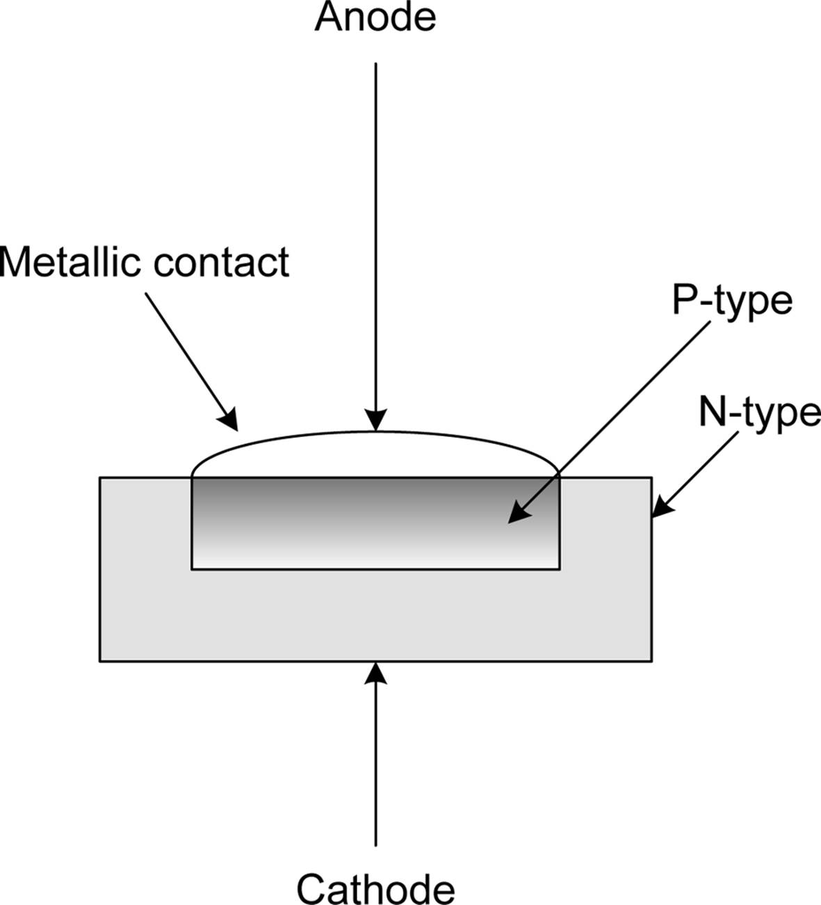
Figure A-49. Structure of a diode made using the fused junction process
Another technique, called planar diffusion or epitaxial growth, involves the diffusion of a P-type region into an N-type semiconductor that sits atop a conductive substrate material. A layer of silicon-dioxide (SiO2) is grown on top of the semiconductor, a section is etched away to expose the P-type material, and finally, a metallic layer is deposited into the space created in the SiO2 layer. This forms the anode of the diode. A metallic layer on the bottom of the substrate forms the cathode terminal of the diode. Figure A-50 shows a cross-section view of a planar diffusion diode.
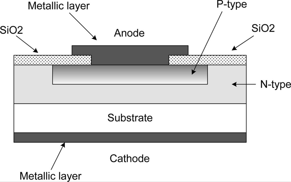
Figure A-50. Structure of a diode created using a planar diffusion process
Special-Purpose Diodes
In addition to small-signal diodes, other types of diodes are available for power rectification that are capable of handling significant amounts of the current. There are also Zener, avalanche, and Schottky types, as well as LEDs and photodiodes.
Zener Diode
A Zener diode is designed to operate in the reverse-bias mode without damage, at least until its maximum current rating is exceeded. When the reverse voltage across a Zener reaches a particular level, as determined at the time the device is fabricated, it will conduct. The I-V curve for a Zener looks similar to that for a standard diode, except that the Zener effect occurs at a much lower reverse voltage than the breakdown in a standard diode. Zener diodes are available in a wide range of voltages and are used to establish reference voltages and as signal limiters. Figure A-51shows how a 5.6V Zener diode can be used to limit a variable voltage.
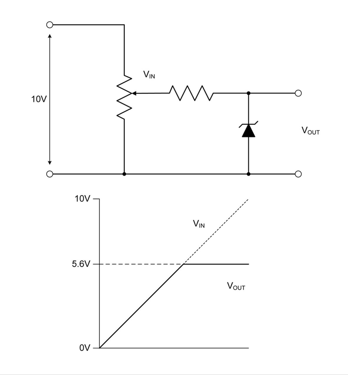
Figure A-51. A Zener diode as a voltage limiter
Avalanche Diode
An avalanche diode is similar to a Zener diode and, actually, the Zener and avalanche diodes exhibit both types of behaviors. But whereas the Zener diode is designed to go into reverse conduction at a specific voltage, the reverse voltage drop in an avalanche diode becomes low once it begins to conduct, and the transition to reverse current flow is very fast. This makes avalanche diodes ideal for protection circuits such as spike protection.
Photodiodes
A photodiode uses the energy of photons to move charge across a junction. A standard P-N junction is photosensitive, but a PIN junction offers improved response speed. A PIN junction comprises P- and N-type material with a thin layer of the element indium in between (hence the I in PIN).
When a photon strikes the junction of a diode, it creates an electron-hole pair. Since the junction has a voltage gradient, the electron is pulled into the N region and the cathode, while the positive hole is swept into the P region toward the anode. The result is a photocurrent.
A photodiode can be designed to operate in either a photovoltaic mode or in a photoconductive mode. In the photovoltaic mode, no bias voltage is applied to the diode, and the device will produce a voltage when it is illuminated due to the photovoltaic effect. In fact, solar cells are just very large photodiodes. In the photoconductive mode, the photodiode is typically reverse biased, and impinging photons will cause a reverse current flow that is proportional to the light level.
Photodiodes are found in a number of applications, ranging from IR remote-control receivers to camera light-level sensors, and from streetlight darkness sensors to the detector in an optical isolator.
LEDs
Light-emitting diodes (LEDs) are legion and can be found almost everywhere. They have largely pushed out the older incandescent technologies for miniature lamps and have started to make significant inroads into residential and commercial lighting applications. They are also cheap, and bags of LEDs can be had for the equivalent of pennies per device.
Internally, an LED is a diode, and it behaves just like any other diode. The big differences can be found in the materials used for the semiconductor and the fact that these materials allow the LED to produce light when current passes through it.
Figure A-52 shows the basics of how an LED produces light. When a bias is applied to the LED, electrons will flow from the N side toward the P side. At the same time, positive holes are moving from the P side toward the N side of the device. The charge carriers move into the junction with different potentials, with the electrons being at a higher potential. When an electron meets a hole, it essentially falls into the hole. In the process, it drops to a lower energy state and a photon is released. In silicon or germanium diodes, the same process occurs when there is current flow, but no light is emitted.

Figure A-52. Production of light in an LED
Transistors
Transistors are a fundamental building block of modern electronics. When they first appeared, they were a radical departure from the vacuum tubes (valves) they started to replace, and they were difficult for many people to understand. But the advantages of the transistor vastly outweighed the unconventional physics of their operation, and the vacuum tube soon started its march into oblivion. Compared to vacuum tubes, transistors are small and compact, use very little power, and don’t generate massive amounts of heat. Without the transistor, it would not have been possible to create integrated circuits and achieve the levels of miniaturization that are common today.
This section is just a light overview of transistors. It is intended to serve as an introduction, not as a comprehensive tutorial. For a more detailed description of what is going on inside a transistor, and for descriptions of other solid-state devices such as UJTs, SCRs, and TRIACs, refer to the texts listed in Appendix C.
Bipolar Junction Transistors
Bipolar junction transistors (BJTs) come in two basic forms: PNP and NPN. The names arise from how these devices are fabricated from P- and N-type semiconductors. Figure A-53 shows a PNP device, and Figure A-54 shows an NPN device.
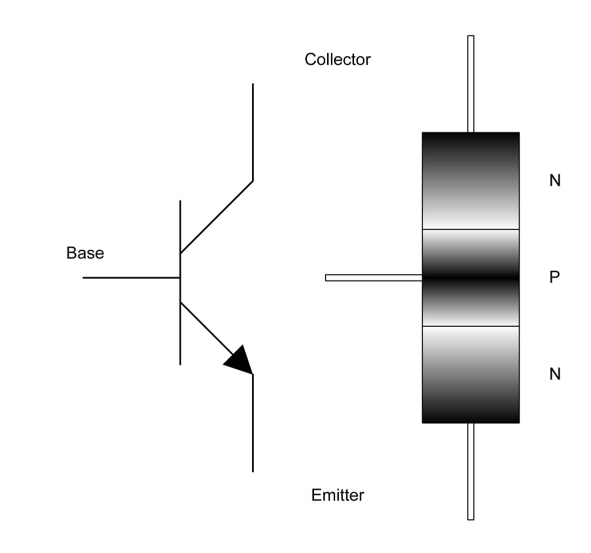
Figure A-53. PNP BJT transistor internal structure
Figure A-54. NPN BJT transistor internal structure
For an NPN transistor, the collector must be more positive than the emitter. The base-emitter and base-collector junctions behave like diodes. In an NPN device, current can flow through base-emitter junction, but the base-collector junction will be reverse biased. A PNP is simply the opposite of an NPN.
A transistor works by modifying the current flow between the emitter and collector terminals by supplying a current to the base terminal. Thus, a small signal current can control a much larger current, and the amount of change in current between the emitter and the collector is a function of the gain (or hfe) of the device.
Internally, the base and emitter terminals of an NPN device behave like a diode. The amount of current flowing through the collector, Ic, is approximately proportional to the amount of current flowing into the base through the base-emitter junction (Ib):
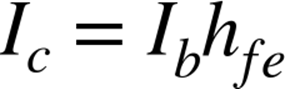
where hfe is the current gain, or beta, of the transistor.
Transistors are nonlinear devices, so the relationship between the input and the output isn’t a straight line. Depending on the hfe and other characteristics, you might need to bias a transistor by applying a small constant DC offset to the base terminal. This will move the input signal into the linear region of the device’s response curve. Without this bias, some part of the input signal might get cut off or distorted.
When a transistor is used as a switch, the idea is to push it into saturation: that is, into a state where the current is flowing freely between the collector and the emitter, and the voltage drop across the terminals is minimal. The trick to achieving saturation is supplying sufficient base current (Ib).
Field-Effect Transistors
A field-effect transistor (FET) differs from a BJT in that a voltage is used to control current flow through the device instead of a current. A FET has three terminals labeled drain, source, and gate. A small voltage change on the gate controls the current flow between the drain and source terminals. As with BJT devices, FETs come in both N and P types, and there are other variations such as MOSFETs, which as based on a metal-oxide semiconductor (the MOS part of MOSFET). Figure A-55 shows a cross-section view of the internal structure of a MOSFET device.
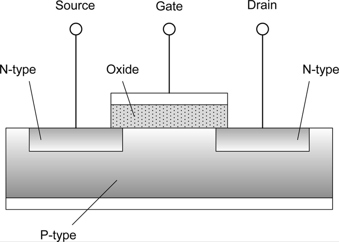
Figure A-55. Internal cross-section of a MOSFET
The primary current flow through a FET is from source to drain. The amount of current flow is determined by the voltage on the gate terminal. What is happening is that the gate voltage modulates the ability of charge carriers (holes and electrons) to move between the source and drain terminals. In this sense, a FET behaves much like a vacuum tube and, in fact, there have been solid-state replacements constructed for some types of vacuum tubes that utilize high-voltage FET devices.
FETs are also used extensively for signal and power switching. A FET that is in the on state (fully conductive) can present a very low resistance to current flow. Analog signal multiplexer chips, such as the Analog Devices ADG506A, use CMOS devices (a type of FET) to select input signals. Each channel has an on resistance of about 280 ohms.
Other applications for power control might utilize high-power MOSFETs to control DC power from a battery. By using a part with a low on resistance, the need for a relay can be eliminated. The IRF710 is an example of a power MOSFET in a TO-220 package. It has a maximum onresistance of 3.6 ohms and is capable of dissipating around 36W of power.
Operational Amplifiers
The operational amplifier (or op amp) is an old device. Early versions existed as vacuum-tube circuits developed for use in early analog computers. An op amp is a high-gain DC-coupled differential amplifier. The op amp schematic symbol uses + and – to denote the noninverting and inverting inputs, respectively, not the polarity of the input voltage.
As it is a differential amplifier, the output of an op amp is an amplified version of the difference between the inputs. In other words, if the noninverting (+) input is higher than the inverting (–) input, then the output of the op amp will be positive. If the inverting input is higher than the noninverting input, then the output will be negative.
Modern op amps are often powered with a bipolar supply, typically +/–15 VDC, although there are op amps available that will work with a single supply voltage. The use of a +/– DC supply allows the op amp to swing its output from – to + in response to the inputs.
Texas Instruments offers a downloadable version of the “Handbook of Operational Amplifier Applications” and Analog Devices offers a free “Op Amp Basics” guide.
Basic Op Amp Circuits
Feedback is used to set the overall gain of the op amp circuit. Without some kind of feedback, a high-gain op amp will respond dramatically to the inputs, with the output going full positive or full negative with just a minute amount of input difference. For this reason, op amps are seldom used without some kind of feedback network.
Op amp circuits can be either inverting or noninverting with regard to the original input. Figure A-56 shows a simple inverting op amp circuit (you can try it with a 741 device or something similar if you want to play with it).
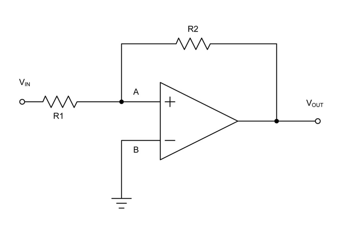
Figure A-56. Simple inverting op amp circuit
The basic principle behind the op amp circuit in Figure A-56 is straightforward: the op amp uses its output to attempt to force the difference between the inputs to zero volts. Since the output is coupled to the input via R2, the output voltage will appear at the junction of R1 and R2 (called asumming junction) and it will be summed with the input voltage through R1. The simple math to determine R1 and R2 looks like this:
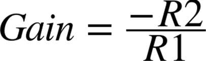
This is equivalent to:
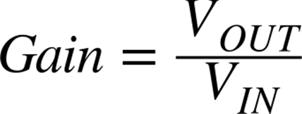
So the voltage gain of the circuit is the ratio of output to input, and it is set by the ratio of R2 to R1. The negative sign on R2 doesn’t mean negative resistance; it simply means that this is an inverting amplifier.
If we wanted a DC amplifier with a gain of 4, perhaps to boost the signal level from a sensor or match the output of our circuit to something else, then we would select a value for R1 and then then solve for R2 with a gain value of 4. In Figure A-57 R1 has been set to 10K ohms, which means R2 will be 40K.
Figure A-57. Inverting op amp circuit with a gain of 4
Since the inverting input is always low (it’s tied to ground), voltage at B will be zero. If A goes positive, then the output will swing negative so that the sum of the voltages at point A in the circuit will also be zero—hence the inversion. Another effect of this is that point A can be considered to be a virtual ground, since the op amp’s output will always try to make it match the inverting input.
The output impedance of an op amp circuit like the ones shown here is typically a fraction of an ohm. The input impedance of an inverting amplifier is dependent on the value of R1. In some situations R1 might end up being small, and this can create impedance matching and input loading problems. The non-inverting form of the op amp circuit shown in Figure A-58 solves this problem.
Figure A-58. Simple non-inverting op amp
Notice in Figure A-58 that the inverting input is supplied by a voltage divider comprised of R1 and R2. This adds a slight twist to the math for computing R1 and R2:
Because op amps are DC amplifiers by design, to work with AC signals and not have to deal with a DC bias hitching a ride on the input or output requires the use of coupling capacitors, which were covered in “Capacitive Coupling”.
Specialized Op Amps
There are many varieties of op amps available. Some have very fast response times, and others are capable of handling large amounts of output current. Still others feature extremely low noise operation or low current consumption, or have been designed to minimize the amount of external circuitry required.
The LM386 is a good example of an op amp with a specialized output section that requires a minimal amount of external components. It is intended primarily as an audio amplifier. Figure A-59 shows the pin-out of the DIP package.
Figure A-59. The LM386 op amp IC
The circuit shown in Figure A-60 can drive an 8-ohm speaker directly, and because the output is coupled to the speaker with a capacitor, there need not be too much concern about stray DC on the input damaging the speaker. This little circuit is handy to have around if you need to trace an audio signal through a live circuit (in this case, an input coupling capacitor would be a necessity), check the output of a signal generator circuit, or integrate an audio output into something that didn’t originally have one. Kits are readily available for LM386 amplifier modules in the $10 (USD) range.
Figure A-60. Audio amplifier using an LM386
Noise
Noise is the bane of electronic circuits, particularly those that deal with low-level signals. In general, noise is any unwanted spurious or periodic signal or voltage that might interfere with the intended operation of a circuit. It might be switching spikes from a nearby relay or power contactor, or it could be stray 60 Hz picked up from nearby appliances or power lines. It might even be a local AM radio station or a ham-radio operator with a high-power rig. This section describes some simple ways to deal with noise.
Noise Sources
Noise can arise from many sources. Low-frequency noise, in the form of spikes and stray AC, is often the result of either power line spikes, inductive coupling, or a load switching on and off somewhere in the circuit. It can also occur when the ground return has a slight resistance, perhaps due to a poor connection or even corrosion. RF interference (RFI) can be a problem with wireless data links and other types of radio frequency devices, and under certain conditions, a strong radio signal can be detected and reproduced by an audio amplifier. If the transmitter is mistuned, and it’s not your transmitter, there might not be much that can be done except to complain about it. However, in many cases, the solution is as simple as making sure that things are correctly shielded and grounded.
AC Line Noise
To deal with a noisy AC power line, such as the mains from a wall socket, you can use a filter, such as the one shown in Figure A-61. This is an off-the-shelf module that sells for about $20 (USD), and most major distributors carry items like this. If you disassemble old surplus equipment, you can often find one of these tucked away inside.
Figure A-61. AC power line filter module
Some IEC-type power cord socket assemblies have a line filter built in, such as the unit shown in Figure A-62. These are available for about $2 each from distributors such as Jameco (see Appendix D).
Figure A-62. Modular IEC power cable connector with built-in line filter
Both the filter module shown in Figure A-61 and the integrated module shown in Figure A-62 actually contain a surprising amount of circuitry inside. Figure A-63 shows what is tucked into a typical filter module like the one shown in Figure A-62.
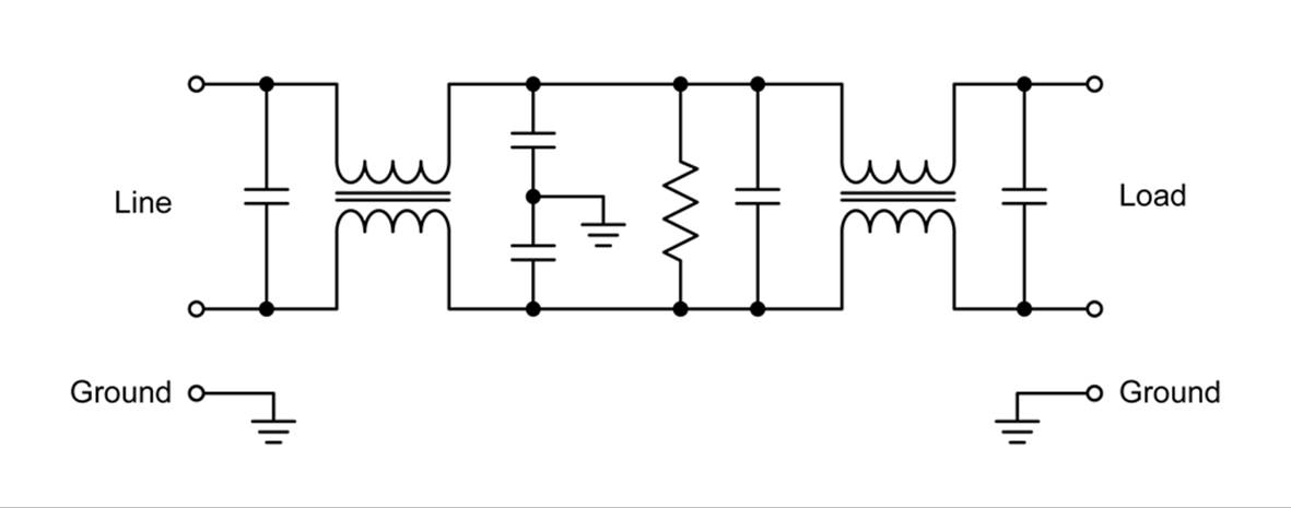
Figure A-63. AC line filter module schematic
This type of filter is designed to suppress unwanted signals at 100 KHz and above without interfering with the 60 Hz AC main. Because spikes typically have fast rise times equivalent to a high-frequency signal, the filter will help to suppress these. The arrangement of capacitors and inductors presents a significant insertion loss to both differential noise and common mode noise.
Although it is possible to build a filter from some capacitors, it’s generally not worth the effort. For a few dollars, you can get something already built and tested.
AC Ripple
A small residual amount of AC on a DC power-supply line is referred to as AC ripple. In some cases, it might be small enough to not cause a problem, but in other cases it can introduce an annoying AC hum (in the case of audio), it can throw off a measurement from a sensor, or it can cause an actuator to misbehave. Cheap wall plug-in-type power supplies (covered in Chapter 5) can sometimes exhibit a significant amount of ripple. Of course, the ideal solution would be to use a better power supply, but sometimes you just have to work with whatever is on hand.
“Passive Filtering” describes a basic single-pole low-pass RC filter. These are suitable for use as ripple filters, provided that the current through the filter is relatively low. The reason is the resistor. Referring to Figure A-44, if you use an R with a value of 33 ohms and a C with a value of 100 μF, you’ll get a filter with a cut-off frequency of about 48 Hz. This is well below the typical 60 Hz AC encountered in the US. Ideally, you would want to keep the value of R as low as possible, to minimize the voltage drop through the filter and thus reduce the amount of power the resistor will need to dissapate.
Spurious Noise
Spurious noise and transient signals can occur when an unshielded signal line passes to close to something that is generating a significant electromagnetic field. Solenoids can cause problems, as can poorly shielded DC motors, transformers, and the wiring of circuits that might be carrying large amounts of current.
POWER SUPPLY MYSTERY
Once, long ago, I worked as a test engineer for a company that produced switching-mode power supplies. One model of power supply was routinely failing final quality control (QC) tests, but the failure happened only when the supply was operating at or near maximum current load. We tried many things to attempt to isolate and resolve the problem. We investigated the transformer between the high-voltage and low-voltage sides of the supply (see Chapter 5 for an overview of what’s inside a switching-mode power supply). We checked out the opto-coupler that provided the voltage level feedback to the high-voltage oscillator. We looked at every possibility, but nothing seemed to be wrong. The supplies simply failed and shut themselves down at high load levels when they should have continued to run.
After exhausting everything we could think of, someone noticed that a wire that connected one part of the low-voltage circuit to another section happened to be routed neatly under the transformer. Because the units operated at about 20 KHz, the transformer wasn’t very large, and it was also unshielded. Just on a hunch, we moved the wire out from under the transformer and the unit behaved flawlessly. The wire, which happened to be the voltage sense line for the feedback circuit, was picking up the field from the transformer and inductively coupling the 20 KHz signal into the feedback circuit. Moving the wire solved the problem.
Logic devices can also introduce switching transients onto a DC power supply line, and for this reason, TTL-type logic typically employs small ceramic capacitors, with values of 0.01 and 0.1 μF commonly seen in circuits that operate at 50 MHz or less. These are also called bypass capacitors, and they are physically mounted close the IC and are connected between the Vcc (V+) pin and ground. Fairchild Semiconductor application note AN-363 discusses power supplies, noise, and decoupling topics in logic circuits.
An arrangement of diodes called a diode clamp can be used to limit the voltage levels of transient spikes on the input of a circuit, as shown in Figure A-64. The idea here is that the forward voltage drops of D1 and D2, and D3 and D4, are summed, and since a typical silicon diode has a drop of about 0.7V, the diodes will not conduct until a spike exceeds 1.4V, either positive or negative.
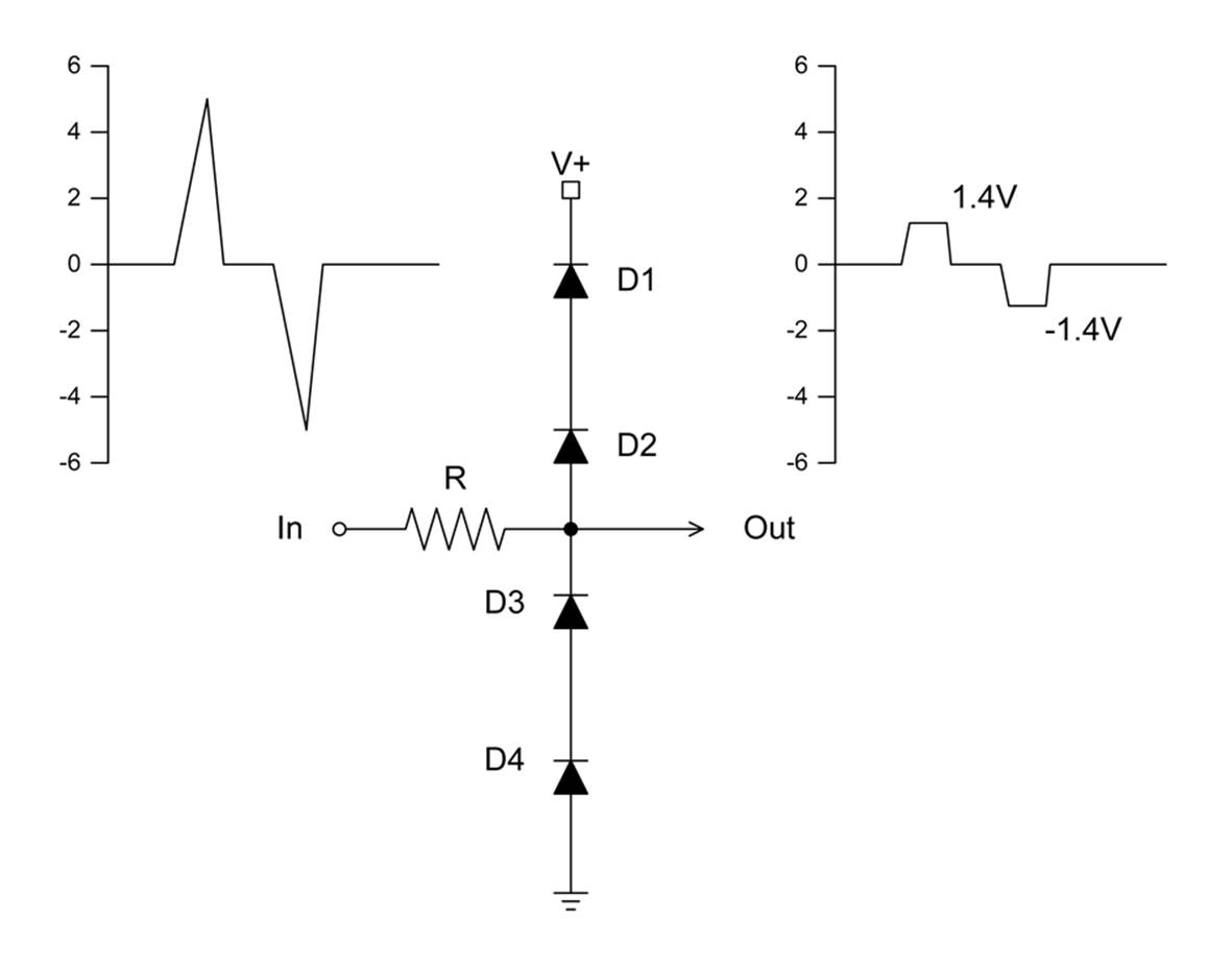
Figure A-64. Simple input protection with a diode clamp circuit
The R in the circuit shown in Figure A-64 is there to act as a current limiter, just in case the diodes are forward biased with enough current to damage them. The value of R should be high enough to prevent damage to the diode but low enough so as not to introduce a large voltage drop. If the input needs to have a greater range than +/– 1.4V, then Zener diodes might be a better choice. Finally, while the diode clamp circuit can prevent damage to components in the subsequent circuit, it still doesn’t eliminate all of the spike. A capacitor can be used to smooth out the remains of the transient signal, but the ideal solution is to find the source of the transients and eliminate them.
RF Noise and RFI
If you suspect you might have an RFI problem, you should check to make sure that antenna cables are shielded, low-level signal lines are either shielded or employ twisted pair wiring (or both), and the shield grounds really are connected to ground. Mounting sensitive circuits in a grounded metal enclosure is also good.
When it comes to RFI, ground means a solid connection to the earth ground return. The negative terminal on a battery is not ground, and a power supply may, or may not, tie the negative terminal to ground. A wall power supply with only two outlet prongs and no ground pin will have a floating negative, whereas a bench power supply will typically have a terminal specifically for ground. If a device is operating such that it has no reference to real ground, it is effectively floating, and it will be susceptible to strong RFI and other noise. Connecting it to a real ground provides the return path needed to shunt the noise away.
You can also use an RC or RLC filter to block unwanted RF. An inductor will exhibit a higher reactance to high frequencies than to lower ones, and something as simple as a ferrite bead or a small choke (like the one shown in Figure 8-35) can block RFI on a DC signal line. An RC low-pass filter like the circuit shown in Figure A-44 can also be used to shunt unwanted high-frequency signals to ground.
Note that putting a filter on a signal line that is carrying something other than a slowly changing DC level or a low-frequency signal can cause unwanted side effects with the signal itself. A filter can distort the waveform of square waves and pulses, resulting in increased rise and fall times with an RC filter, and ringing with a choke or RLC filter. Basically, any signal with a fast rise time will be impacted by the filter. An AC signal (such as AC power or audio) will experience a phase shift, and in the case of an audio signal, some of the high-frequency harmonics might be supressed if the cut-off frequency for the filter is low enough.
Recommended Reading and Further Exploration
This appendix is just a high-level summary of the very deep field of electronics. The texts listed in Appendix C contain much more information, and I suggest that you look there to seek additional knowledge. I’ve listed some of the texts here that I feel are particularly relevant to the topics contained in this appendix.
The Art of Electronics by Paul Horowitz and Winfield Hill and Electronics by Allan Hambley both cover all of the topics presented in this appendix. The Electrical Engineering Handbook (Richard Dorf, Ed.) is a valuable reference that packs in a lot of detailed information, but it is mostly advanced material and can be a bit cryptic in places. Another text, written at a more introductory level, can help you make sense of what you might find is the The Electrical Engineering Handbook.
If you want to learn to work with op amps, Walter G. Jung’s IC Op-Amp Cookbook is a good place to start. In addition to the theory (which is also covered in other texts), this book contains many interesting example circuits, all of which can be assembled on a solderless breadboard if you want to work with them.
The ARRL Handbook, an official publication of the American Radio Relay League, is my own go-to book when I want to find some information about RLC circuits and antennas. The Radio Handbook by William I. Orr is another favorite of mine. Both of these books are packed with hands-on how-to projects, and although most of the projects and circuits are oriented toward radio communications, they are treasure troves of information about inductors, tuned circuits, and high-frequeny electronics in general.
You can also find massive amounts of information free on the Internet. Some of what you find might not be entirely complete or totally accurate, but for the most part, enough eyes have been on it that the errors tend to get corrected. If I feel too lazy to pull down a book and elect instead to use Google to find something, I always make it a point to find more than one source and compare them.
All materials on the site are licensed Creative Commons Attribution-Sharealike 3.0 Unported CC BY-SA 3.0 & GNU Free Documentation License (GFDL)
If you are the copyright holder of any material contained on our site and intend to remove it, please contact our site administrator for approval.
© 2016-2026 All site design rights belong to S.Y.A.