Programming the 65816 Including the 6502, 65C02, and 65802 (1986)
Appendices
A. 65x Signal Description
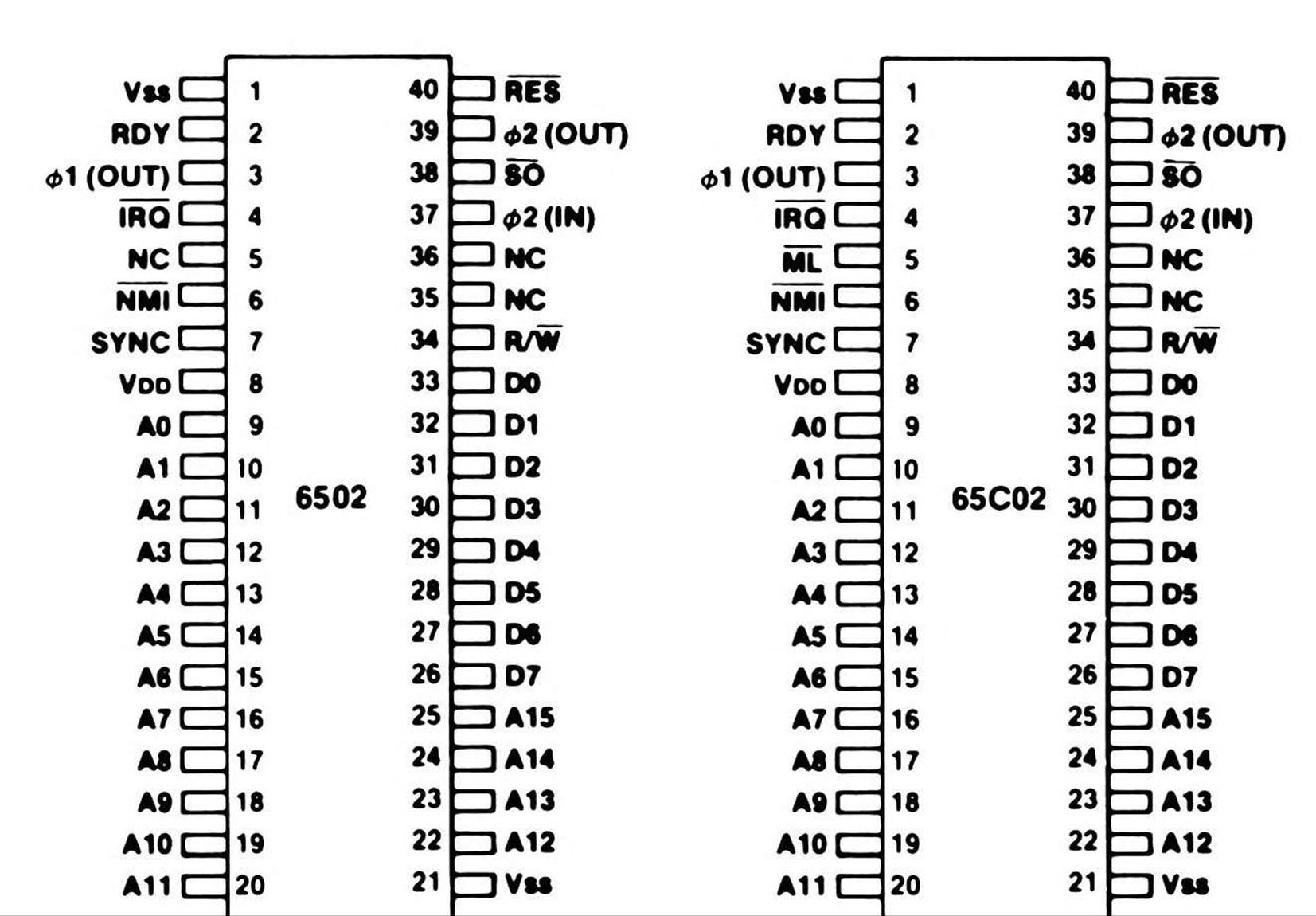
The four standard 65x parts considered in this book—the 6502, 65C02, 65802, and 65816—are each housed in a 40-pin dual in-line package. There are also a number of special versions of the basic parts, versions with external clocks, fewer address pins, one-chip computers with on-board RAM and ROM, and with quadrature clocks. These are not considered here; refer to the appropriate manufacturer's literature for details about these special chips.
This appendix describes the pin signals found on the four standard parts—the pins that connect the processor to the external system. Many of them are common to all processors, some are unique to each.
The descriptions are meant to satisfy the programmer with a general interest in the system implementation; the engineer implementing a 65x system should consult the manufacturer's data sheets for more detailed information.
To begin with, refer to Figure A.1, which illustrates the pin configurations of the four different processors.
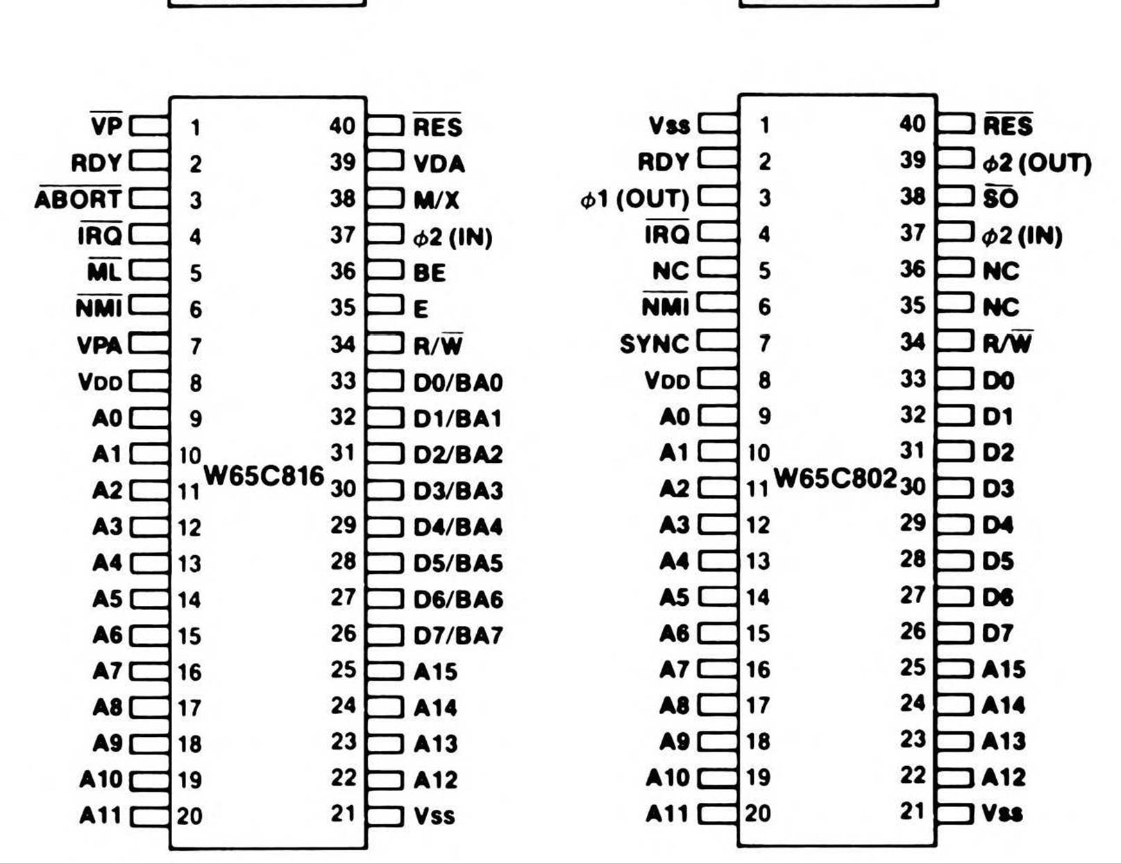
Figure A.I. 65x Pinouts.
6502 Signals
The 6502 defines the basic set of signals.
Address Bus
Pins A0 - A15 are the address lines. Every time an address is generated—opcode fetch, operand read, intermediate address, or effective address of a read or write operation—the binary value of the address appears on these pins, A0 representing the low-order bit of the address, and A15 representing the high-order bit. These outputs are TTL compatible.
Clock Signals
All of the 65x series processors operate on a two-phase external cycle; a 65x processor's frequency, expressed in Megahertz, or millions of cycles per second, is also its memory-access cycle time. The 6502 has an internal clock generator based on the phase zero input signal, a time base typically provided by a crystal oscillator. The two output signals, phase one and phase two, are derived from this signal. Phase one goes high when phase zero is low; phase two goes low on the rising edge of phase one.
Data Bus
Pins D0-D7 are the data lines; these eight pins form a bi-directional data bus to read and write data between the processor and memory and the peripheral devices. Like the address lines, the outputs can drive one standard TTL load.
Data Bus Enable
This controls the three-state output buffers of the processor; it normally is enabled by the phase two output, effectively disabling the output buffers during phase one; this frees the bus for access by other devices during phase one. By pulling DBE low, the buffers may be disabled externally.
Read/Write
R/W' is high when data is being read from memory or peripherals into the processor, low when the processor is writing data. When in the low state, data and address lines have valid data and addresses.
Ready
The RDY signal enables the processor to be single-stepped on all cycles except write cycles. When enabled during phase one, the processor is halted and the address lines maintain the current address; this lets the processor interface with lower-speed read-only memory devices, and can also be used in direct memory access implementations.
Interrupt Request
The IRQ' signal requests that an interrupt-service cycle be initiated. This signal is connected to peripheral devices that are designed to be interrupt-driven. This is the maskable interrupt signal, so the interrupt disable flag in the status register must be zero for the interrupt to be effective. The RDY signal must be high for an interrupt to be recognized. IRQ' is sampled during phase 2.
Non-maskable Interrupt
NMI' is basically identical to IRQ', except that it causes an unconditional interrupt when it is asserted, and control vectors through the NMI' vector rather than IRQ'.
Set Overflow
When this line goes low on the trailing edge of phase one, the overflow flag in the processor status register is set.
Sync
This line goes high during phase one of those cycles that are opcode fetches. When used with the RDY signal, this allows hardware implementation of a single-step debugging capability.
Reset
RESET' reinitializes the processor, either at power-up or to restart the system from a known state. RESET' must be held low for at least two cycles after a power down. When it is asserted, an interrupt-like service routine begins (although the status and program counter are not stacked), with the result that control is transferred through the RESET' vector.
65C02 Signals
The 65C02 pinout is identical to the 6502, with the exception of memory lock and notes described below.
Memory Lock
The ML' output signal assures the integrity of read-modify-write instructions by signaling other devices, for example, other processors in a multiprocessor environment, that the bus may not be claimed until completion of the read-modify-write operation. This signal goes low during the execution of the memory-referencing (non-register operand) ASL, DEC, INC, LSR, ROL, ROR, TRB, and TSB instructions.
Notes
The 65C02, unlike the 6502, responds to RDY during a write cycle as well as a read, halting the processor.
Response of the 65C02 to a reset is different from the 6502 in that the 65C02's program counter and status register are written to the stack. Additionally, the 65C02 decimal flag is cleared after reset or interrupt; its value is indeterminate after reset and not modified after interrupt on the 6502.
When an interrupt occurs immediately after the fetch of a BRK instruction on the 6502, the BRK is ignored; on the 65C02, the BRK is executed, then the interrupt is executed.
Finally, the 65C02 R/W' line is high during the modify (internal operation) cycle of the read-modify-write operations; on the 6502, it is low.
65802 Signals
The 65802 signals are by definition 6502 pin-compatible. The 65C02 ML' (memory lock) signal is not on the standard pin-out, although it is available as a special-order mask option. Like the 6502, and unlike the 65C02, the 65802 does not write to the stack during a reset.
Some of the enhancements of the 65C02 are available on the 65802 in the native mode, while in emulation mode the system behaves as a 6502. R/W' is low during the modify cycle of read-modify-write cycles in the emulation mode; high in the native mode.
65816 Signals
Most of the signals behave as on the 65802, with the following additions and changes:
Bank Address
The most important difference on the 65816 is the multiplexing of the bank address (BA0-BA7) with the data pins (D0-D7). During phase two low, the bank address is valid; during phase two high, data is read or written on the same pins. The bank address must be latched during phase one to provide a valid twenty-four bit address when concatenated with A0-A15.
Vector Pull
The VP' signal is asserted whenever any of the vector addresses ($00:FFE4-FFEF, $00:FFF4-FFFF) are being accessed as part of an interrupt-type service cycle. This lets external hardware modify the interrupt vector, eliminating the need for software polling for interrupt sources.
Abort
The ABORT' input pin, when it is asserted, causes the current instruction to be aborted. Unlike an interrupt, none of the registers are updated and the instruction quits execution from the cycle where the ABORT' signal was received. No registers are modified. In other words, the processor is left in the state it was in before the instruction that was aborted. Control is shifted to the ABORT' vector after an interrupt-like context-saving cycle.
The ABORT' signal lets external hardware abort instructions on the basis of undesirable address bus conditions; memory protection and paged virtual memory systems can be fully implemented using this signal.
ABORT' should be held low for only one cycle; if held low during the ABORT interrupt sequence, the ABORT interrupt will be aborted.
Valid Program Address and Valid Data Address
The VPA and VDAsignals extend the concept of the SYNC signal. Together, these two pins encode one of four possible internal processor states, based on the type of memory being accessed:
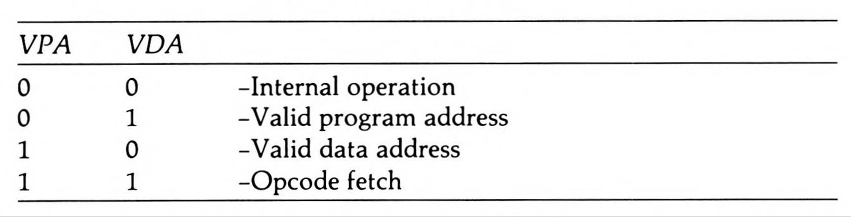
During internal operations, the output buffers may be disabled by external logic, making the address bus available for transparent direct memory access. Also, since the 65816 sometimes generates a false read during instructions that cross page boundaries, these may be trapped via these two signals if this is desirable. Note, however, that addresses should not be qualified in emulation mode if hardware such as the Apple // disk controller is used, which requires false read to operate.
The other states may be used for virtual memory implementation and high-speed data or instruction cache control. VPA and VDA high together are equivalent to the 6502 SYNC output.
Memory and Index
These two signals are multiplexed on pin 38. M is available during phase zero, X during phase one. These signals reflect the contents of the status register m and x flags, allowing (along with E described below) external logic to fully decode opcode fetches.
As a mask option, the 65816 may be specified with the 6502 SET OVERFLOW signal instead of the M/X signal.
M and X are invalid for the instruction cycle following the REP, SEP, and PLP instruction execution; this cycle is the opcode fetch cycle of the next instruction.
Emulation
The E signal reflects the state of the processor's e flag; depending on whether or not the processor is in emulation mode or not, external system compatibility features (such as memory mapping or system speed) could be enabled or disabled.
Bus Enable
This signal replaces the data bus enable signal of the 6502; when asserted, it disables the address buffers and R/W' as well as the data buffers.
All materials on the site are licensed Creative Commons Attribution-Sharealike 3.0 Unported CC BY-SA 3.0 & GNU Free Documentation License (GFDL)
If you are the copyright holder of any material contained on our site and intend to remove it, please contact our site administrator for approval.
© 2016-2026 All site design rights belong to S.Y.A.