Programming the 65816 Including the 6502, 65C02, and 65802 (1986)
Appendices
B. 65x Series Support Chips
There are a plethora of companion chips for the 65x processors. The ones every assembly language programmer runs into eventually are serial and parallel input/output (I/O) chips. The 65x family serial I/O controller is the 6551 Asynchronous Communication Interface Adapter (ACIA), while the the simplest parallel I/O controller is the 6521 Peripheral Interface Adapter (PIA).
As the architecture section of this book has already noted, the 65x microprocessors have memory-mapped I/O, not special I/O opcodes. That is, they assign each input and each output device one or more memory locations. An output device's status registers can be tested to determine if the device is ready to send a unit of data. Conversely, an input device's status registers can be tested to determine if a unit of data has arrived and can be read. Writing data is accomplished by storing it to one of the output device's memory locations; reading it is accomplished with a load-register instruction, with its operand one of the input device's memory locations.
One caution: Don't attempt to use any peripheral chips without calling or writing the chip's manufacturer for a data sheet, usually provided for little or no charge. While data sheets are no joy to read, they contain enough information to sooner or later explain the programming problems you will run into, if not on your current project, then on the next one.
The 6551 Serial Chip
You may already be familiar with the 6551 ACIA. There is one controlling the serial port on every Apple //c, and one on the plug-in Apple //e Super Serial Card.
The 6551 features an on-chip baud-rate generator, which lets your program set any of fifteen baud rates from 50 to 19,200. Like most other serial chips, word length, number of stop bits, and parity bit generation and detection can also be set under program control.
As an example, if the Super Serial Card were located, as it commonly is, in the Apple //e's port two, four consecutive memory locations are allocated to the 6551 beginning at $C0A8. The 6551's Transmit/Receive Data Register is located at $C0A8. The current status of the chip (for example, indicating it has received a byte of data) is indicated in the Status Register, located at $C0A9 {see Figure B.1). Two registers are used to initialize the chip. The Command Register, located at SCOAA, is used to set up parity and several other parameters. As Figure B.2 indicates, writing $0B to the Command Register sets up a commonly used set of parameters—no parity, and both the RTS and the DTR lines enabled. The Control Register, located at SCOAB, is used to set up stop bits, word length, and baud rate; as Figure B.3 indicates, writing $1E to the Control Register sets up a commonly used set of parameters—one stop bit, eight-bit data, and communications running at 9600 baud.
So the 6551 is initialized by the 65816 code shown in Fragment B.1.
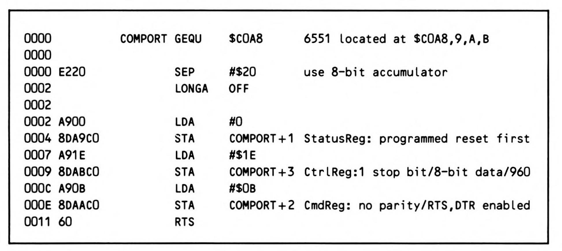
Fragment B.1.
Actually, any value can be written to the status register to cause a programmed reset; this operation is done to reinitialize the I/O registers—the three figures each show the effects on the non-data registers on each of their status bits.
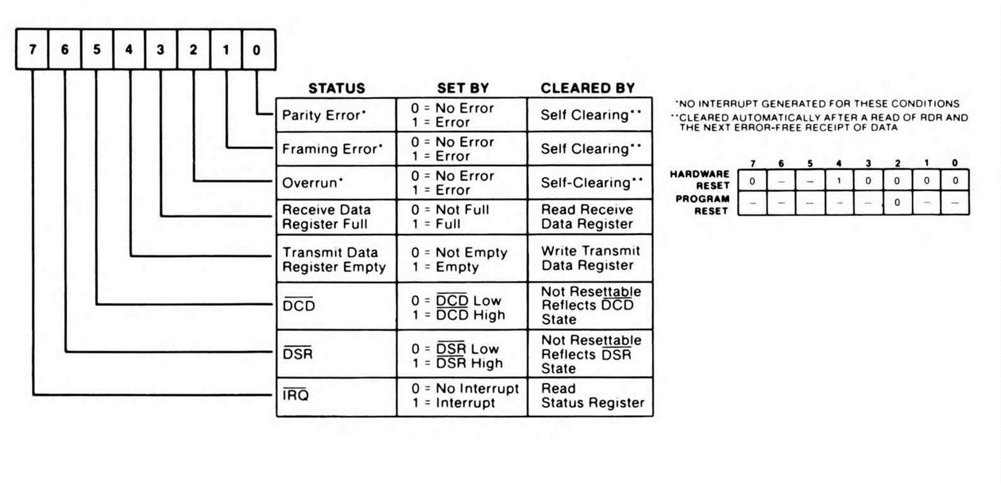
Figure B.l. 6551 Status Register.
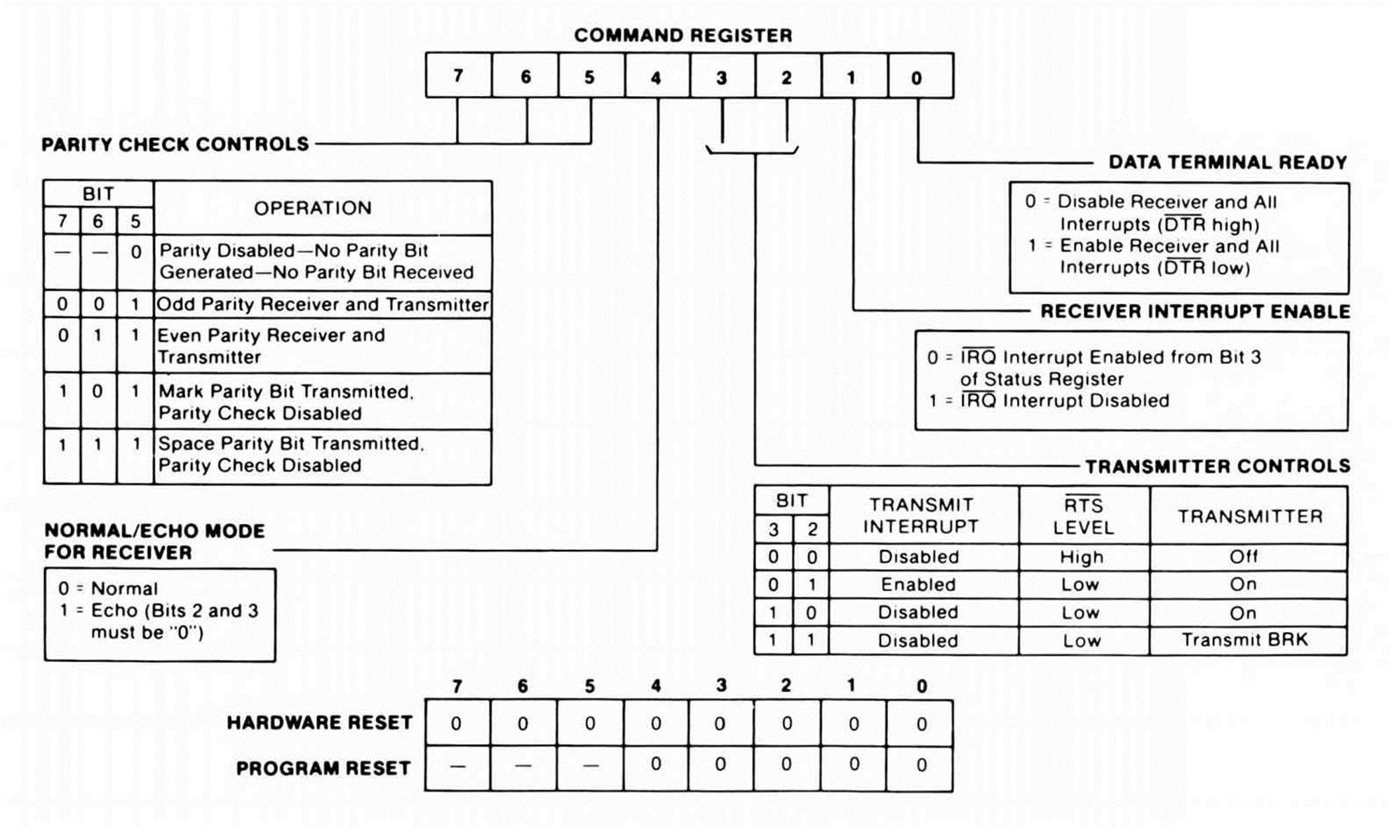
Figure B.2. 6551 Command Register.
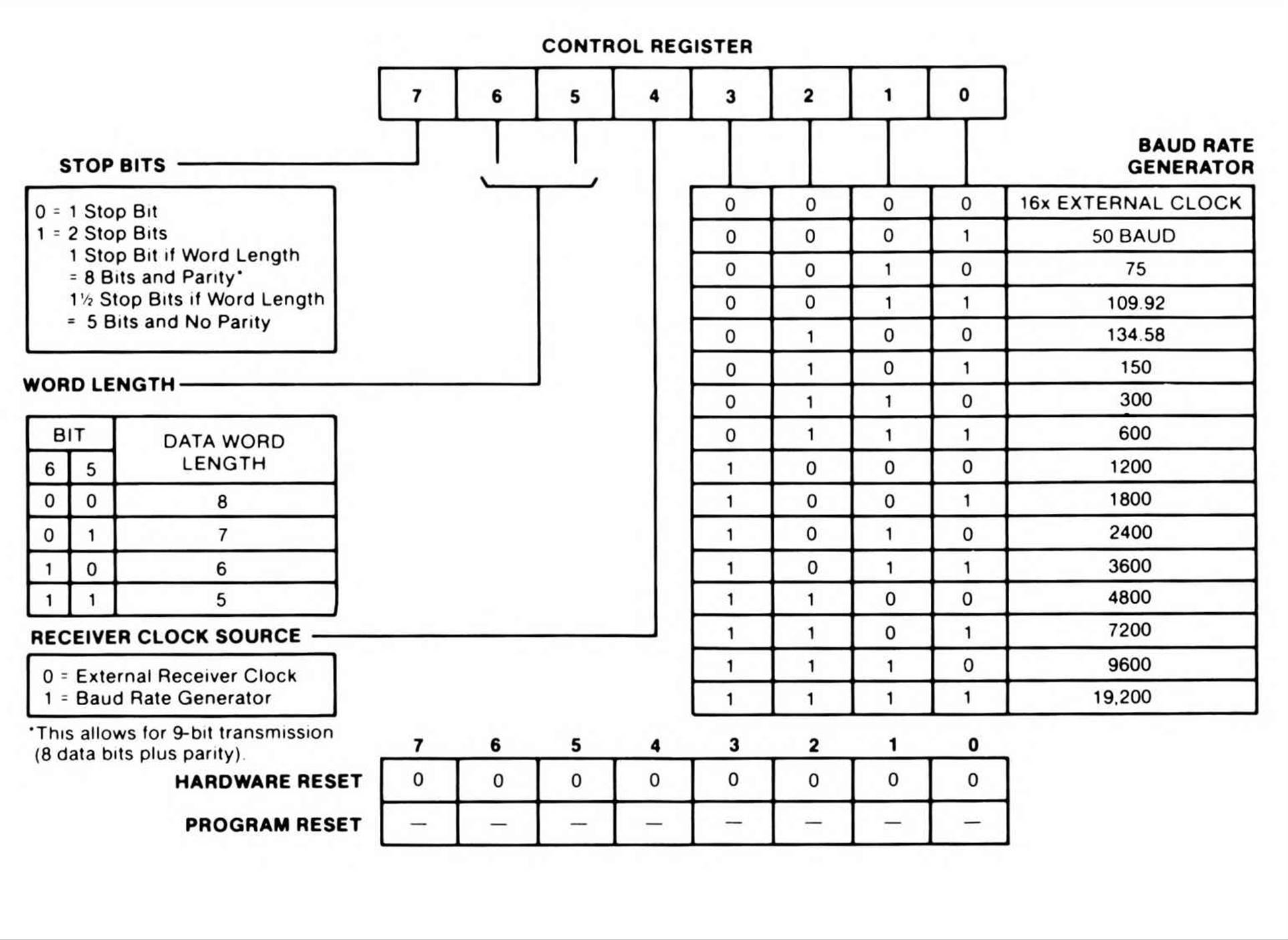
Figure B.3. 6551 Control Register.
When the 6551 connects a computer to a communications line—whether twisted-pair wire at 9600 baud or a modem at 300 baud—reading a byte from the communications line is a matter of (once the 6551 has been initialized) waiting until the status register bit three (receiver data register full) is set, then reading the byte from the data register, as shown in Fragment B.2.
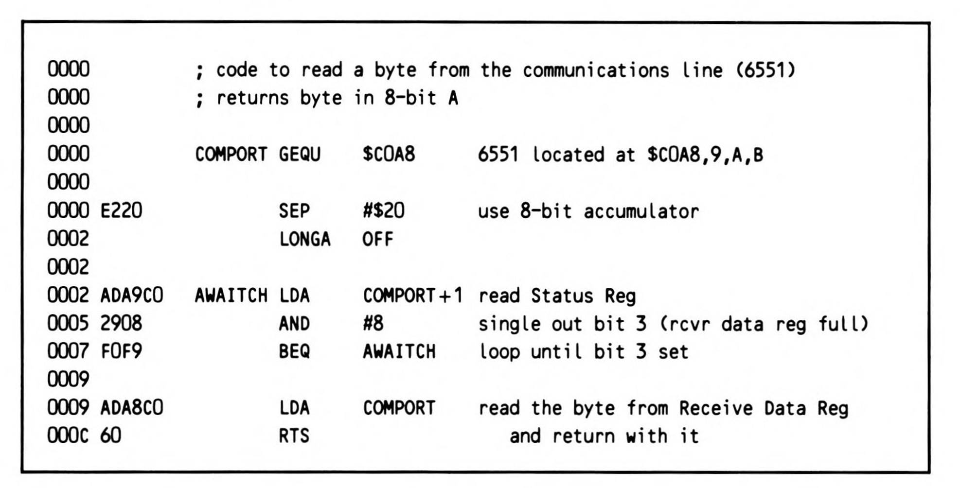
Fragment B.2.
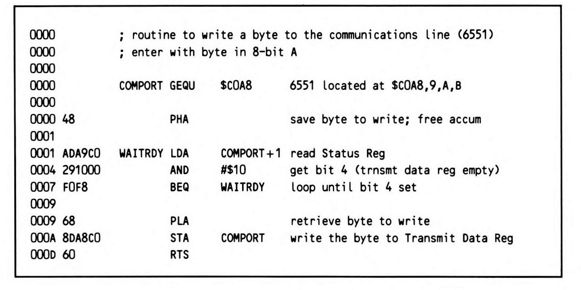
Similarly, as Fragment B.3 shows, writing a byte out to the communications line is a matter of (once the 6551 has been initialized) waiting until the status register bit four (transmitter data register empty) is set, then writing the byte to the data register.
Neither routine does any error checking using the other status register bits.
The 6521 Parallel Chip
The 6521 parallel I/O peripheral interface adapter is used to interface 65x microprocessors with printers, matrix-type keyboards, and other devices. It features two programmable eight-bit bidirectional parallel I/O ports (Ports A and B), any lines of which can be individually set for either reading or writing via a Data Direction Register. Provided all eight lines are set one way, you can either read or write a byte at a time (as opposed to a bit at a time via a serial chip) through the port. For fancy I/O, the 6521 has several "handshake" lines for greater control of I/O.
Like the 6551, the 6521 occupies four address locations (those dependent on the hardwiring of the two Register Select lines). But it has six registers, three for each port: a control register, a data register, and a data direction register. Each port's data register and data direction register are addressed at the same location. Bit two of the port's control register determines which register is connected to that address at any one time: if control register bit two is set, the data register is connected; if control register bit two is clear, the data direction register is connected.
Fragment B.3.
The data direction register is generally initialized for an application just once; then the data register is selected. Each data direction register bit controls the same-numbered bit in the data register: if a data direction register bit is set, the corresponding data register bit becomes an output line; if a data direction register bit is clear, the corresponding data register bit becomes an input line.
Imagine an application in which a printer is wired through a Centronics-compatible printer port to a 6521's port A: the 6521's eight Port A bits are connected to Centronics pins two through nine. Port B is used to control the interface between computer and printer: the 6521's Port B bit zero is connected to the printer's Data Strobe (Centronics pin one); the 6521's Port B bit seven is connected to the printer Busy Line (Centronics pin 11).
The 6521 PIA is automatically initialized on power-up and reset to all be inputs (all registers are cleared). So every program should initialize all the lines it will use, either as inputs or as outputs, every time it is run. In this case, setting up output to the printer means all of Port A needs to be set up as inputs, while Port B bit zero must be initialized as an output and bit seven as an input. Setting up the rest of Port B as inputs is a good habit to protect outside peripherals, as seen in Fragment B.4.
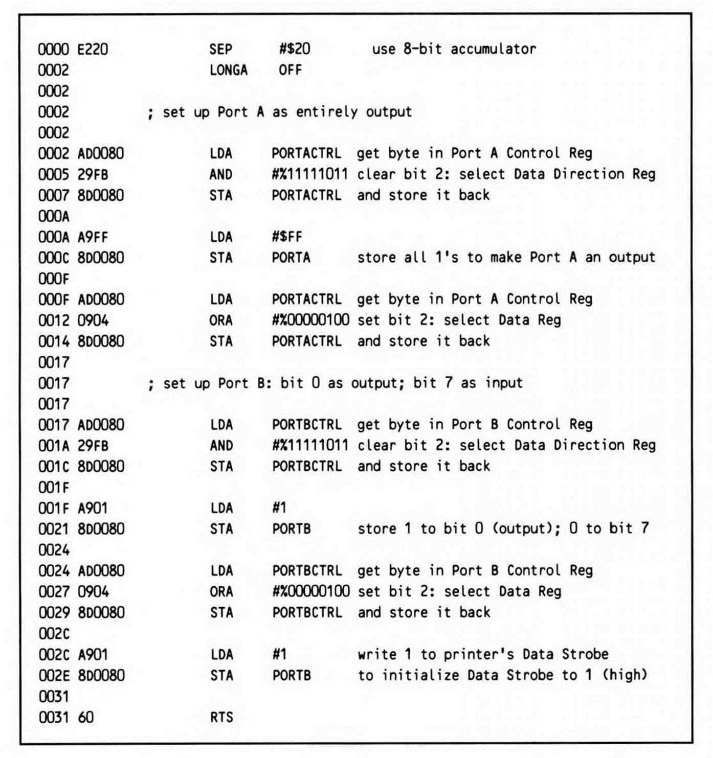
Fragment B.4.
PORTACTRL, PORTA, PORTBCTRL, and PORTB must be elsewhere equated to the addresses at which each is located. The value in the control register is loaded and bit two is ANDed out with the mask, then stored back to choose the data direction register as the chosen register in each port. All ones are stored to Port A's data direction register, selecting all eight lines as outputs. One is stored to Port B's data direction register, selecting bit zero as an output and the rest of the port as inputs. Then the control registers are loaded again, this time ORing bit two back on before re-storing them, to choose the data register as the chosen register in each port. Finally, one is written out Port B to the printer's Data Strobe to initialize the line.
Now bytes can be written to the printer by waiting for a zero on the Printer Busy Line (bit seven of Port B was chosen so that a positive/negative test could be made to test the bit), then storing the byte to be written to Port A, and finally toggling the Data Strobe to zero and then back to one to inform the printer that a new character is ready to be printed.
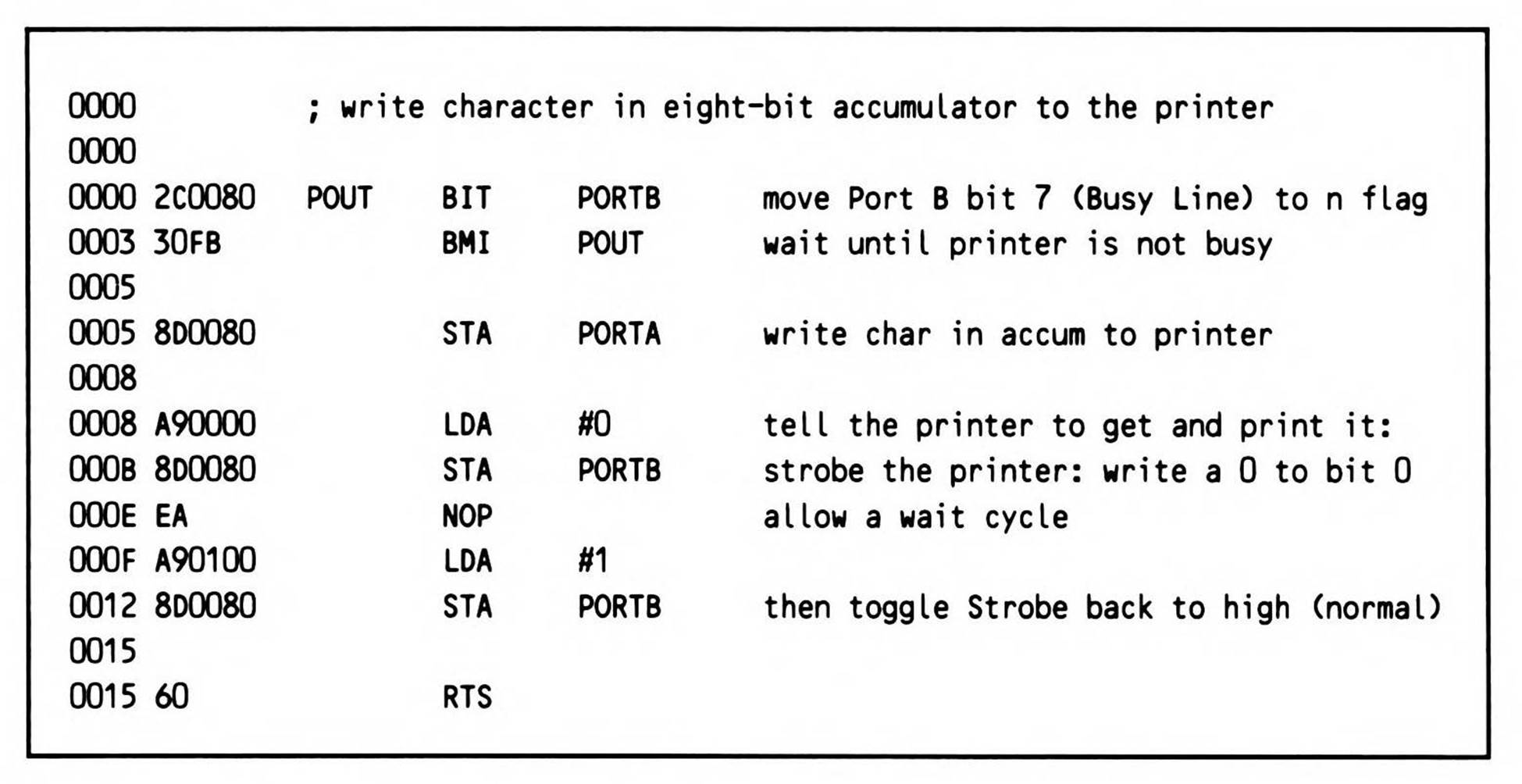
Fragment B.5.
You must be sure, in toggling the Strobe by writing to it, that the zero written to bit seven (zeroes are written to bits one through seven during both writes to Port B) not be read back as though it is a value being sent by the printer's Busy Line indicating the printer is not busy.
Remember that it is always important to have a data sheet for each peripheral support chip you attempt to write code for.
All materials on the site are licensed Creative Commons Attribution-Sharealike 3.0 Unported CC BY-SA 3.0 & GNU Free Documentation License (GFDL)
If you are the copyright holder of any material contained on our site and intend to remove it, please contact our site administrator for approval.
© 2016-2026 All site design rights belong to S.Y.A.