Programming the 65816 Including the 6502, 65C02, and 65802 (1986)
Appendices
E. W65C816 Data Sheet
CMOS W65C816 and W65C802
16-Bit Microprocessor Family
Features
•Advanced CMOS design for low power consumption and increased noise immunity
•Single 3-6V power supply, 5V specified
•Emulation mode allows complete hardware and software compatibility with 6502 designs
•24-bit address bus allows access to 16 MBytes of memory space
•Full 16-bit ALU. Accumulator, Stack Pointer, and Index Registers
•Valid Data Address (VDA) and Valid Program Address (VPA) output allows dual cache and cycle steal DMA implementation
•Vector Pull (VP) output indicates when interrupt vectors are being addressed May be used to implement vectored interrupt design
•Abort (ABORT) input and associated vector supports virtual memory system design
•Separate program and data bank registers allow program segmentation or full 16-MByte linear addressing
•New Direct Register and stack relative addressing provides capability for re-entrant, re-cursive and re-locatable programming
•24 addressing modes—13 original 6502 modes, plus 11 new addressing modes with 91 instructions using 255 opcodes
•New Wait for Interrupt (WAI) and Stop the Clock (STP) instructions further reduce power consumption, decrease interrupt latency and allows synchronization with external events
•New Co-Processor instruction (COP) with associated vector supports co-processor configurations, i.e., floating point processors
•New block move ability
General Description
WDC's W65C802 and W65C816 are CMOS 16-bit microprocessors featuring total software compatibility with their 8-bit NMOS and CMOS 6500-series predecessors The W65C802 is pin-to-pin compatible with 8-bit devices currently available, while the W65C816 extends addressing to a full 16 megabytes. These devices offer the many advantages of CMOS technology, including increased noise immunity, higher reliability, and greatly reduced power requirements. A software switch determines whether the processor is in the 8-bit "emulation" mode, or in the native mode, thus allowing existing systems to use the expanded features.
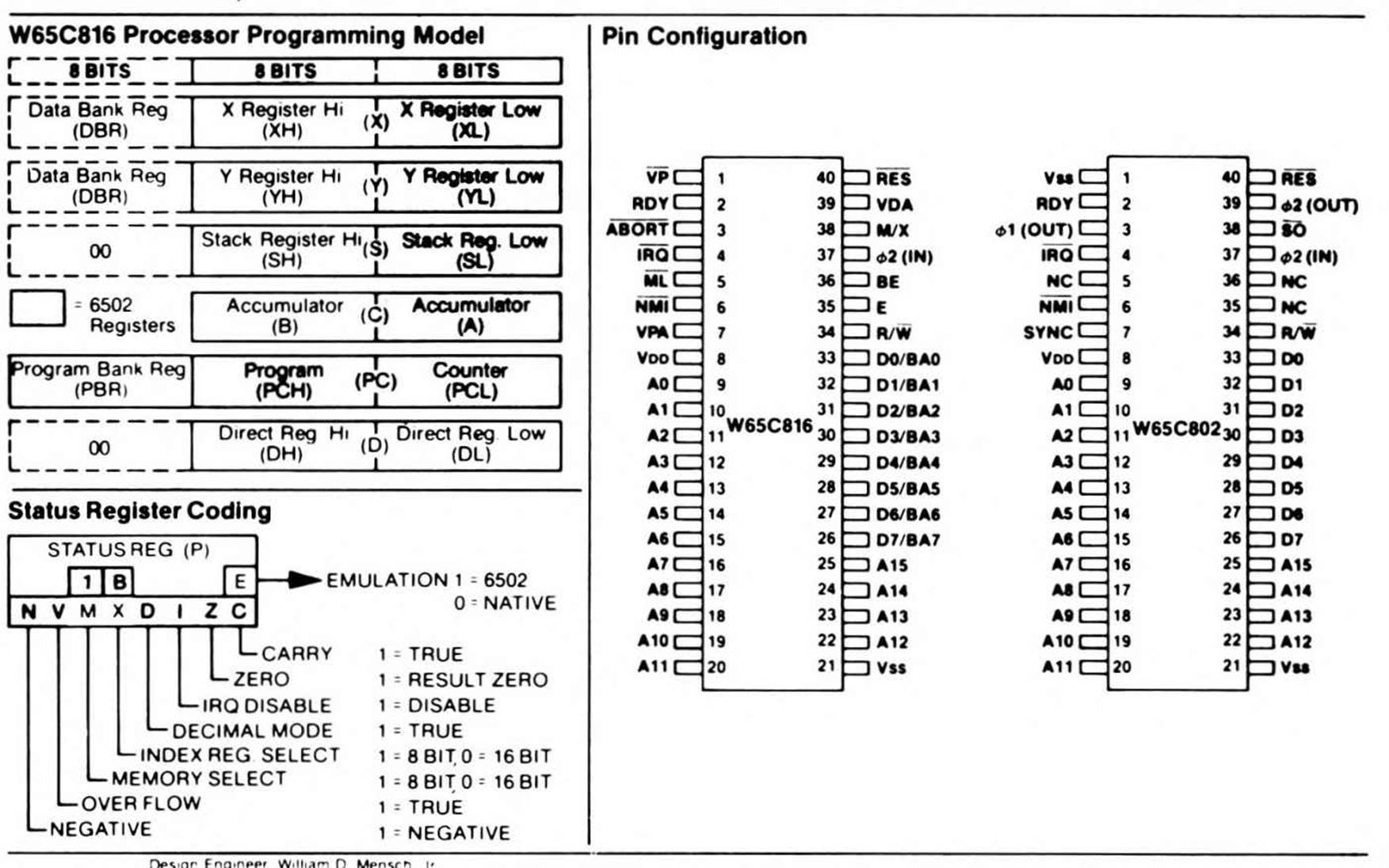
As shown in the processor programming model, the Accumulator, ALU, X and Y Index registers, and Stack Pointer register have all been extended to 16 bits. A new 16-bit Direct Page register augments the Direct Page addressing mode (formerly Zero Page addressing). Separate Program Bank and Data Bank registers allow 24-bit memory addressing with segmented or linear addressing.
Four new signals provide the system designer with many options. The ABORT input can interrupt the currently executing instruction without modifying internal register, thus allowing virtual memory system design.Valid Data Address (VDA) and Valid Program Address (VPA) outputs facilitate dual cache memory by indicating whether a data segment or program segment is accessed. Modifying a vector is made easy by monitoring the Vector Pull (VP) output.
Note: To assist the design engineer, a Caveat and Application Information section has been included within this data sheet.

Advance Information Data Sheet:
This is advanced information and specifications are subject to change without notice.
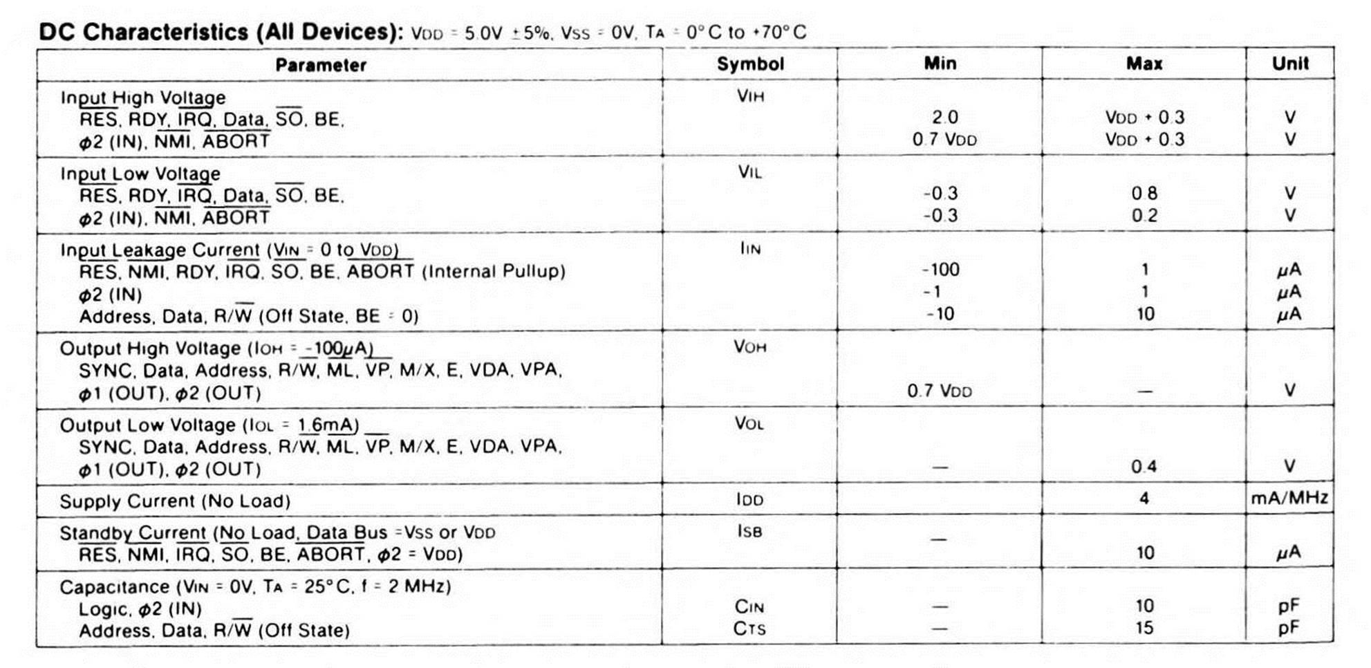
Absolute Maximum Ratings: (Note 1)
This device contains input protection against damage due to high static voltages or electric fields, however, precautions should be taken to avoid application of voltages higher than the maximum rating.
Notes:
1. Exceeding these ratings may cause permanent damage. Functional operation under these conditions is not implied.
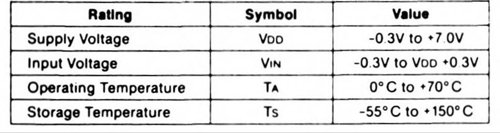
Pin Function Table
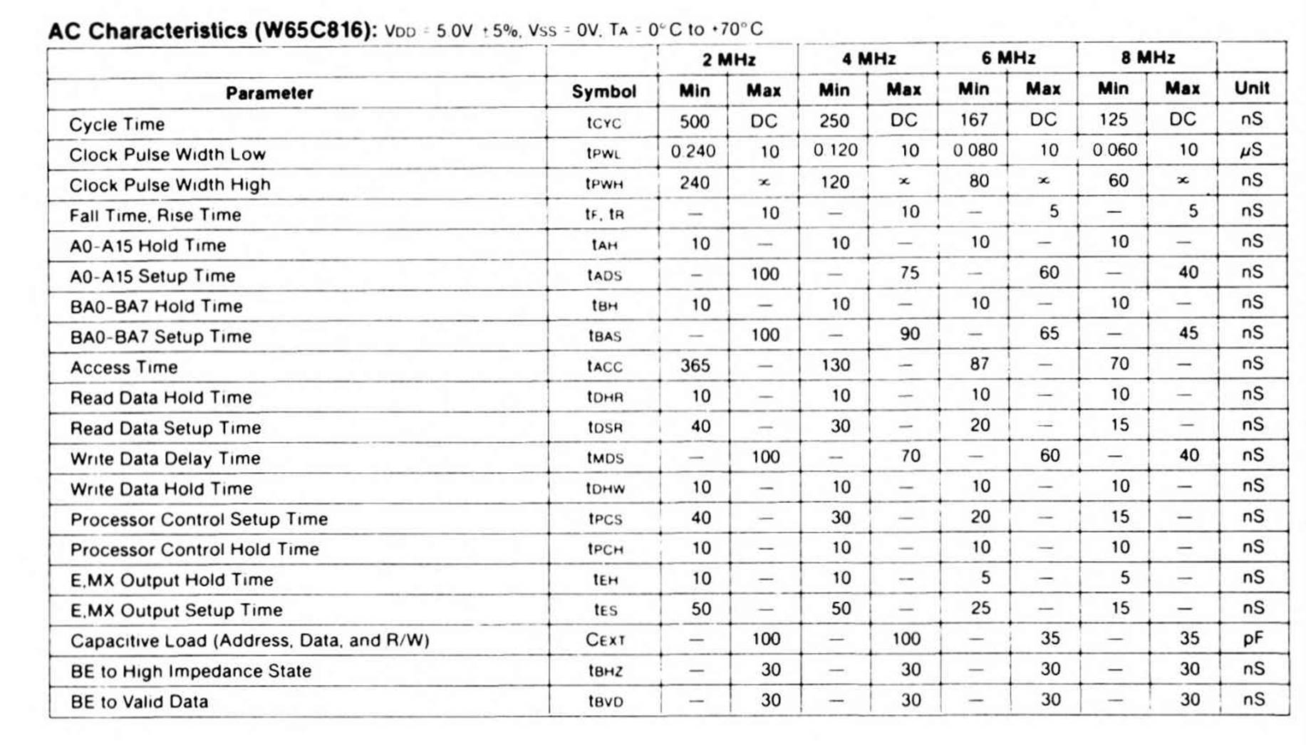
Timing Notes:
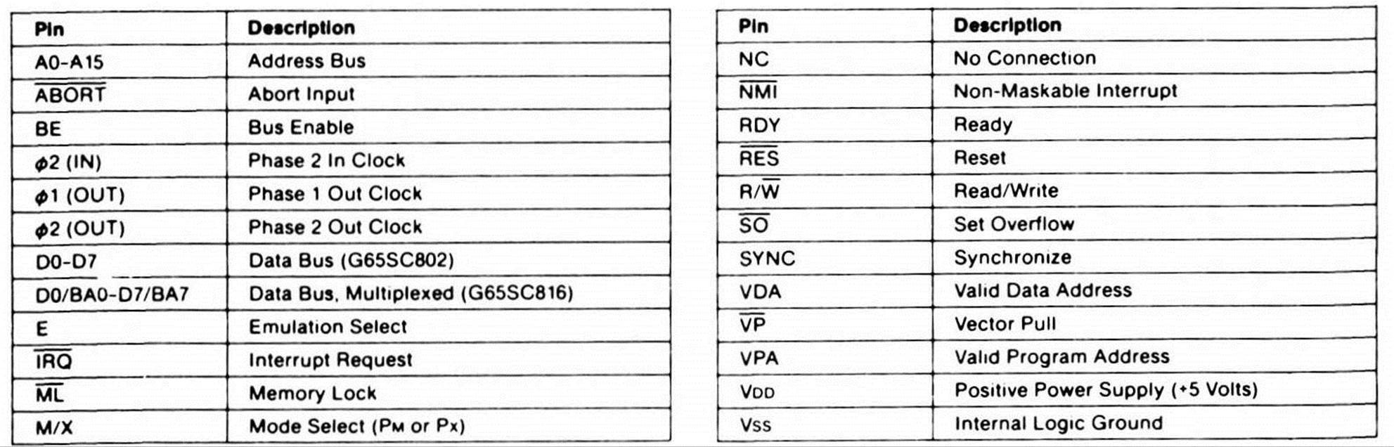
1 Voltage levels are VL < 0.4V. VH > 2.4V
2 Timing measurement points are 0.8V and 2.0V
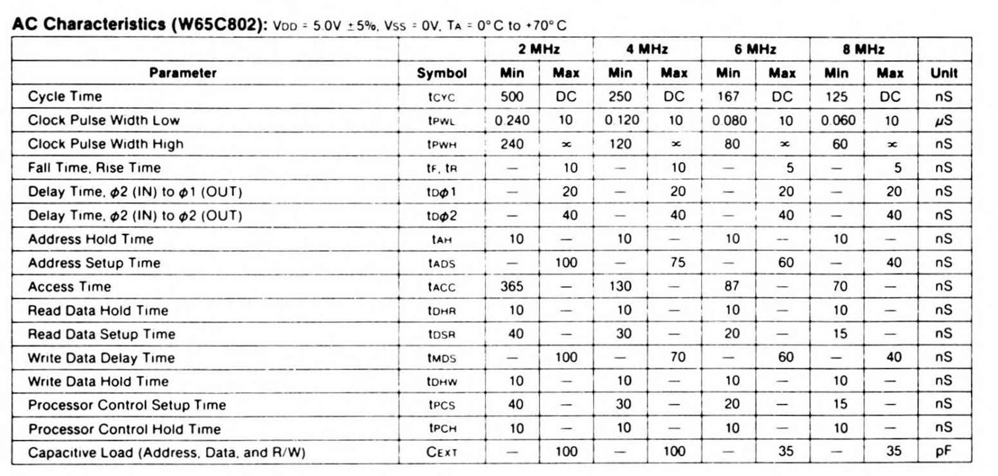
Timing Notes:
1. Voltage levels are VL < 0.4V, VH > 2.4V
2. Timing measurement points are 0.8V and 2.0V
Functional Description
The W65C802 offers the design engineer the opportunity to utilize both existing software programs and hardware configurations, while also achieving the added advantages of increased register lengths and faster execution times. The W65C802’s “ease of use” design and implementation features provide the designer with increased flexibility and reduced implementation costs. In the Emulation mode, the W65C802 not only offers software compatibility, but is also hardware (pin-to-pin) compatible with 6502 designs... plus it provides the advantages of 16-bit internal operation in 6502-compatible applications. The W65C802 is an excellent direct replacement microprocessor for 6502 designs.
The W65C816 provides the design engineer with upward mobility and software compatibility in applications where a 16-bit system configuration is desired. The W65C816's 16-bit hardware configuration, coupled with current software allows a wide selection of system applications. In the Emulation mode, the W65C816 offers many advantages, including full software compatibility with 6502 coding. In addition, the W65C816's powerful instruction set and addressing modes make it an excellent choice for new 16-bit designs.
Internal organization of the W65C802 and W65C816 can be divided into two parts: 1) The Register Section, and 2) The Control Section. Instructions (or opcodes) obtained from program memory are executed by implementing a series of data transfers within the Register Section. Signals that cause data transfers to be executed are generated within the Control Section. Both the W65C802 and the W65C816 have a 16-bit internal architecture with an 8-bit external data bus.
Instruction Register and Decode
An opcode enters the processor on the Data Bus, and is latched into the Instruction Register during the instruction fetch cycle. This instruction is then decoded, a long with timing and interrupt signals, to generate the various Instruction Register control signals.
Timing Control Unit (TCU)
The Timing Control Unit keeps track of each instruction cycle as it is executed. The TCU is set to zero each time an instruction fetch is executed, and is advanced at the beginning of each cycle for as many cycles as is required to complete the instruction. Each data transfer between registers depends upon decoding the contents of both the Instruction Register and the Timing Control Unit.
The Timing Control Unit keeps track of each instruction cycle as it is executed. The TCU is set to zero each time an instruction fetch is executed, and is advanced at the beginning of each cycle for as many cycles as is required to complete the instruction. Each data transfer between registers depends upon decoding the contents of both the Instruction Register and the Timing Control Unit.
Arithmetic and Logic Unit (ALU)
All arithmetic and logic operations take place within the 16-bit ALU. In addition to data operations, the ALU also calculates the effective address for relative and indexed addressing modes. The result of a data operation is stored in either memory or an internal register. Carry, Negative. Overflow and Zero flags may be updated following the ALU data operation.
Internal Registers (Refer to Programming Model)
Accumulators (A, B, C)
The Accumulator is a general purpose register which stores one of the operands, or the result of most arithmetic and logical operations. In the Native mode (E=0). when the Accumulator Select Bit (M) equals zero, the Accumulator is established as 16 bits wide (A + B = C). When the Accumulator Select Bit (M) equals one. the Accumulator is 8 bits wide (A). In this case, the upper 8 bits (B) may be used for temporary storage in conjunction with the Exchange Accumula tor (XBA) instruction.
Data Bank Register (DBR)
During modes of operation, the 8-bit Data Bank Register holds the default bank address for memory transfers. The 24-bit address is composed of the 16-bit instruction effective address and the 8-bit Data Bank address. The register value is multiplexed with the data value and is present on the Data/Address lines during the first half of a data transfer memory cycle for the W65C816. The Data Bank Register is initialized to zero during Reset.
Direct (D)
The 16-bit Direct Register provides an address offset for all instructions using direct addressing. The effective bank zero address is formed by adding the 8-bit instruction operand address to the Direct Register. The Direct Register is initialized to zero during Reset.
Index (X and Y)
There are two Index Registers (X and Y) which may be used as general purpose registers or to provide an index value for calculation of the effective address. When executing an instruction with indexed addressing, the microprocessor fetches the opcode and the base address, and then modifies the address by adding the Index Register contents to the address prior to performing the desired operation. Pre-indexing or post-indexing of indirect addresses may be selected. In the Native mode (E=0), both Index Registers are 16 bits wide (providing the Index Select Bit (X) equals zero). If the Index Select Bit (X) equals one. both registers will be 8 bits wide, and the high byte is forced to zero.
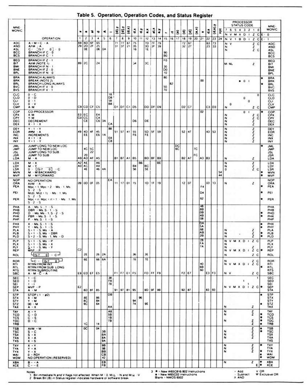
Processor Status (P)
The 8-bit Processor Status Register contains status flags and mode select bits. The Carry (C). Negative (N). Overflow (V). and Zero (Z) status flags serve to report the status of most ALU operations. These status flags are tested by use of Conditional Branch instructions. The Decimal (D). IRQ Disable (I), Memory/Accumulator (M), and Index (X) bits are used as mode select flags. These flags are set by the program to change microprocessor operations.
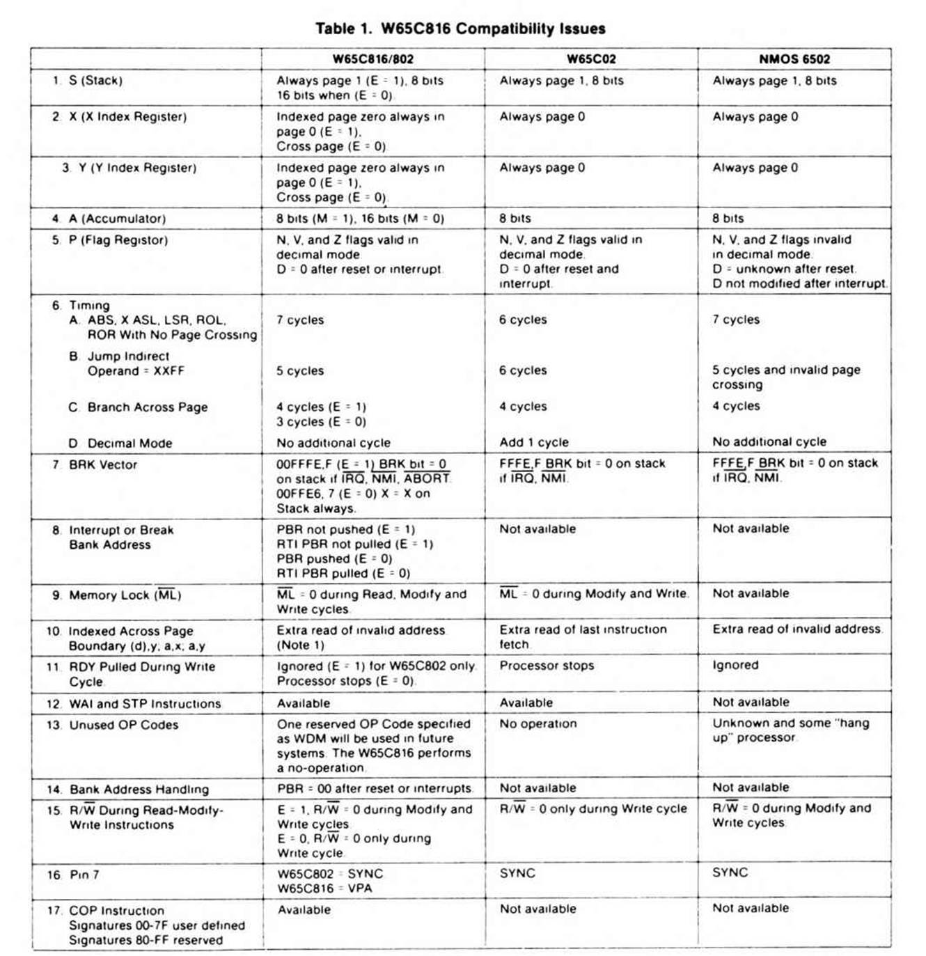
The Emulation (E) select and the Break (B) flags are accessible only through the Processor Status Register. The Emulation mode select flag is selected by the Exchange Carry and Emulation B its (XCE) instruction. Table 1, W65C802 and W65C816 Mode Comparison, illustrates the features of the Native (E=0) and Emulation (E=1) modes The M and X flags are always equal to one in the Emulation mode. When an interrupt occurs during the Emulation mode, the Break flag is written to stack memory as bit 4 of the Processor Status Register.
Program Bank Register (PBR)
The 8-bit Program Bank Register holds the bank address for all instruction fetches. The 24-bit address consists of the 16-bit instruction effective address and the 8-bit Program Bank address. The register value is multiplexed with the data value and presented on the Data/Address lines during the first half of a program memory read cycle. The Program Bank Register is initialized to zero during Reset. The PHK instruction pushes the PBR register onto the Stack.
Program Counter (PC)
The 16-bit Program Counter Register provides the addresses which are used to step the microprocessor through sequential program instructions. The register is incremented each time an instruction or operand is fetched from program memory.
Stack Pointer (S)
The Stack Pointer is a 16-bit register which is used to indicate the next available location in the stack memory area. It serves as the effective address in stack addressing modes as well as subroutine and interrupt processing. The Stack Pointer allows simple implementation of nested subroutines and multiple-level interrupts. During the Emulation mode, the Stack Pointer high-order byte (SH) is always equal to one. The bank address for all stack operations is Bank zero.
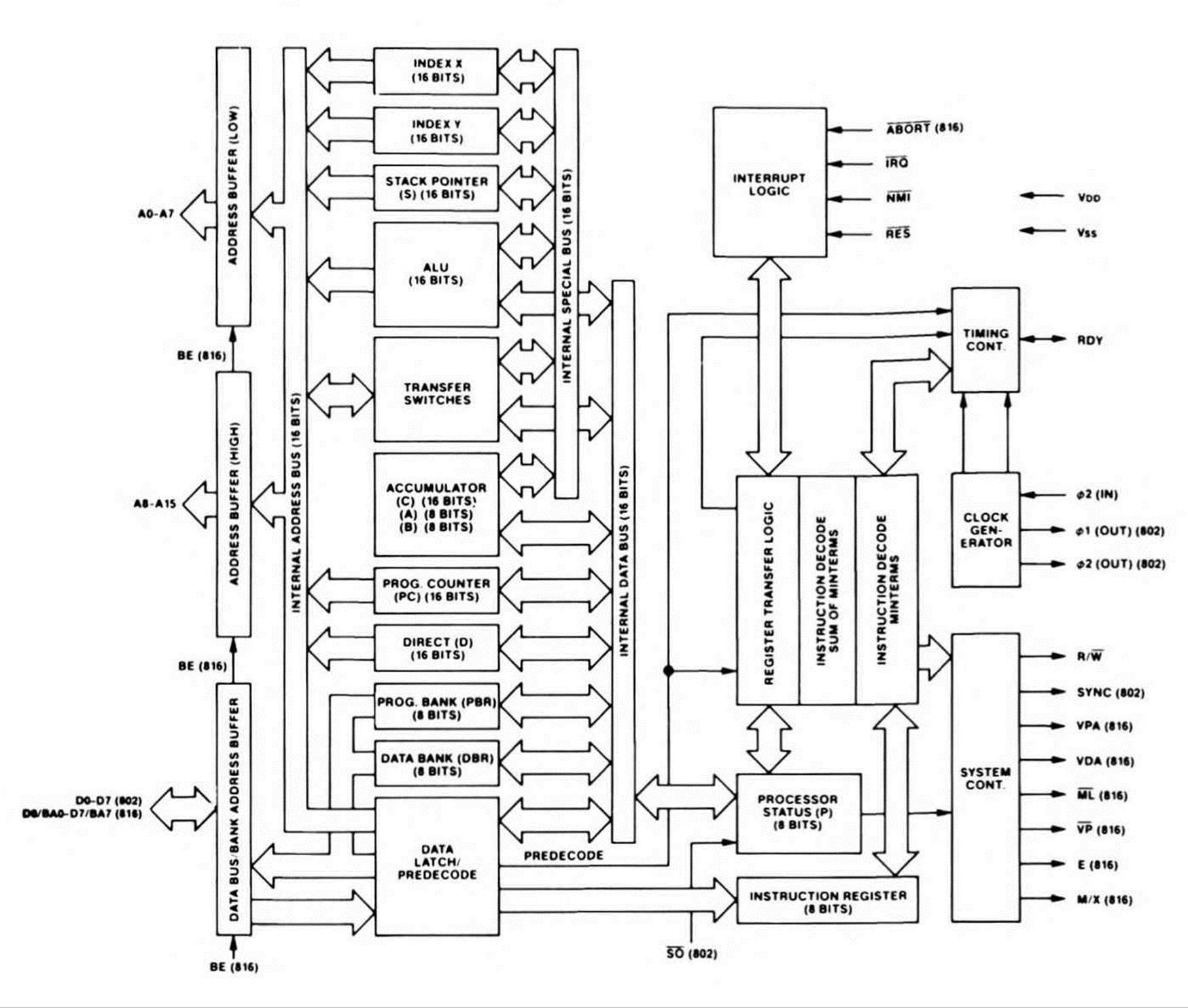
Figure 1. Block Diagram — Internal Architecture
Signal Description
The following Signal Description applies to both the G65SC802 and the G65SC816 except as otherwise noted.
Abort (ABORT)— G65SC816
The Abort input is used to abort instructions (usually due to an Address Bus condition). A negative transition will inhibit modification of any internal register during the current instruction. Upon completion of this instruction, an interrupt sequence is initiated. The location of the aborted opcode is stored as the return address in stack memory. The Abort vector address is 00FFF8.9 (Emulationmode) or 00FFE8.9 (Native mode). Note that ABORT is a pulse-sensitive signal, i.e. an abort will occur whenever there is a negative pulse (or level) on the ABORT pm during a Φ2clock.
Address Bus (A0-A15)
These sixteen output lines form the Address Bus for memory and I/O exchange on the Data Bus. When using the G65SC816. the address lines may be set to the high impedance state by the Bus Enable (BE) signal.
Bus Enable (BE)— W65C816
The Bus Enable input signal allows external control of the Address and Data Buffers, as well as the R/W signal. With Bus Enable high, the R/W and Address Buffers are active. The Data/Address Buffers are active during the first half of every cycle and the second half of a write cycle When BE is low. these buffers are disabled. Bus Enable is an asynchronous signal.
Data Bus (D0-D7)—W65C802
The eight Data Bus lines provide an 8-bit bidirectional Data Bus for use during data exchanges between the microprocessor and external memory or peripherals. Two memory cycles are required for the transfer of 16-bit values.
Data/Address Bus (D0/BA0-D7/BA7)—W65C816
These eight lines multiplex address bits BA0-BA7 with the data value. The address is present during the first half of a memory cycle, and the data value is read or written during the second half of the memory cycle. Two memory cycles are required to transfer 16-bit values. These lines may be set to the high impedance state by the Bus Enable (BE) signal.
Emulation Status (E)—W65C816
The Emulation Status output reflects the state of the Emulation (E) mode flag in the Processor Status (P) Register. This signal may be thought of as an opcode extension and used for memory and system management.
Interrupt Request (IRQ)
The Interrupt Request input signal is used to request that an interrupt sequence be initiated. When the IRQ Disable (I) flag is cleared, a low input logic level initiates an interrupt sequence after the current instruction is completed. The Wait for Interrupt (WAI) instruction may be executed to ensure the interrupt will be recognized immediately. The Interrupt Request vector address is OOFFFE.F (Emulation mode) or 00FFEE.F (Native mode). Since IRQ is a level-sensitive input, an interrupt will occur if the interrupt source was not cleared since the last interrupt. Also, no interrupt will occur if the interrupt source is cleared prior to interrupt recognition.
Memory Lock (ML)- W65C816
The Memory Lock output may be used to ensure the integrity of Read-Modify-Write instructions in a multiprocessor system. Memory Lock indicates the need to defer arbitration of the next bus cycle. Memory Lock is low during the last three or five cycles of ASL, DEC, INC, LSR, ROL, ROR, TRB, and TSB memory referencing instructions, depending on the state of the M flag.
Memory/Index Select Status (M/X)—W65C816
This multiplexed output reflects the state of the Accumulator (M) and Index (X) select flags (bits 5 and 4 of the Processor Status (P) Register. Flag M is valid during the Phase 2 clock negative transition and Flag X is valid during the Phase 2 clock positive transition. These bits may be thought of as opcode extensions and may be used for memory and system management.
Non-Maskable Interrupt (NMI)
A negative transition on the NMI input initiates an interrupt sequence. A high-to-low transition initiates an interrupt sequence after the current instruction is completed. The Wait for Interrupt (WAI) instruction may be executed to ensure that the interrupt will be recognized immediately. The Non-Maskable Interrupt vector address is OOFFFA,B (Emulation mode) or OOFFEA,B (Native mode). Since NMI is an edge-sensitive input, an interrupt will occur if there is a negative transition while servicing a previous interrupt. Also, no interrupt will occur if NMI remains low.
Phase 1 Out (Φ1 (OUT))—W65C802
This inverted clock output signal provides timing for external read and write operations. Executing the Stop (STP) instruction holds this clock in the low state.
Phase 2 In (Φ2 (IN))
This is the system clock input to the microprocessor internal clock generator (equivalent to Φ0 (IN) on the 6502). During the low power Standby Mode. Φ2 (IN) should be held in the high state to preserve the contents of internal registers.
Phase 2 Out (Φ2 (OUT))—W65C802
This clock output signal provides timing for external read and write operations. Addresses are valid (after the Address Setup Time TADS)) following the negative transition of Phase 2 Out Executing the Stop (STP) instruction holds Phase 2 Out in the High state
Read/Write (R/W)
When the R/W output signal is in the high state, the microprocessor is reading data from memory or I/O. When in the low state, the Data Bus contains valid data from the microprocessor which is to be stored at the addressed memory location. When using the W65C816. the R/W signal may be set to the high impedance state by Bus Enable (BE).
Ready (RDY)
This bidirectional signal indicates that a Wait for Interrupt (WAI) instruction has been executed allowing the user to halt operation of the microprocessor. A low input logic level will halt the microprocessor in its current state (note that when in the Emulation mode, the W65C802 stops only during a read cycle). Returning RDY to the active high state allows the microprocessor to continue following the next Phase 2 In Clock negative transition. The RDY signal is internally pulled low following the execution of a Wait for Interrupt (WAI) instruction, and then returned to the high state when a RES, ABORT, NMI, or IRQ external interrupt is provided. This feature may be used to eliminate interrupt latency by placing the WAI instruction at the beginning of the IRQ servicing routine. If the IRQ Disable flag has been set. the next instruction will be executed when theIRQ occurs. The processor will not stop after a WAI instruction if RDY has been forced to a high state. The Stop (STP) instruction has no effect on RDY.
Reset (RES)
The Reset input is used to initialize the microprocessor and start program execution. The Reset input buffer has hysteresis such that a simple R-C timing circuit may be used with the internal pullup device. The RES signal must be held low for at least two clock cycles after VOD reaches operating voltage. Ready (RDY) has no effect while RES is being held low. During this Reset conditioning period, the following processor initialization takes place:
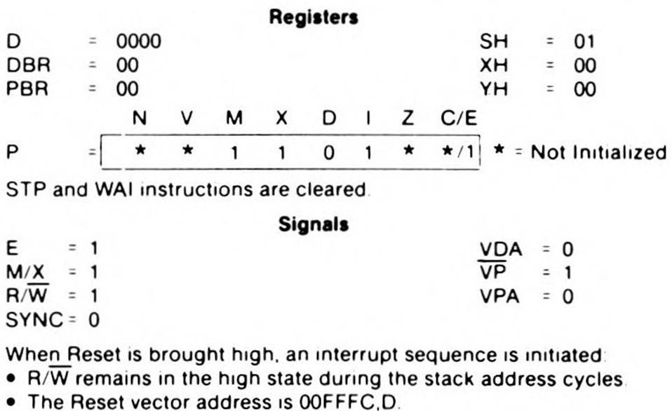
When Reset is brought high, an interrupt sequence is initiated:
•R/W remains in the high state during the stack address cycles.
•The Reset vector address is 00FFFC.D.
Set Overflow (SO)— W65C802
A negative transition on this input sets the Overflow (V) flag, bit 6 of the Processor Status (P) Register.
Synchronize (SYNC)—W65C802
The SYNC output is provided to identify those cycles during which the microprocessor is fetching an opcode. The SYNC signal is high during an opcode fetch cycle, and when combined with Ready (RDY). can be used for single instruction execution.
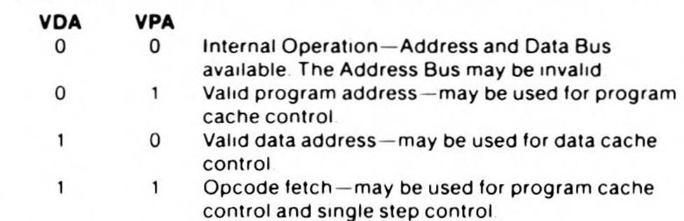
Valid Data Address (VDA) and
Valid Program Address (VPA)-G65SC816
These two output signals indicate valid memory addresses when high (logic 1), and must be used for memory or I/O address qualification.
VOD and Vss
Vdd is the positive supply voltage and Vss is system logic ground Pin 21 of the two Vss pins on the W65C802 should be used for system ground.
Vector Pull (VP—) W65C816
The Vector Pull output indicates that a vector location is being addressed during an interrupt sequence. VP is low during the last two interrupt sequence cycles, during which time the processor reads the interrupt vector. The VP signal may be used to select and prioritize interrupts from several sources by modifying the vector addresses.
Note 1. See Caveat section for additional information.
W65C802 and W65C816
Microprocessor Addressing Modes
The W65C816 is capable of directly addressing 16 MBytes of memory. This address space has special significance within certain addressing modes, as follows:
Reset and Interrupt Vectors
The Reset and Interrupt vectors use the majority of the fixed addresses between OOFFEO and OOFFFF.
Stack
The Stack may use memory from 000000 to OOFFFF. The effective address of Stack and Stack Relative addressing modes will always be within this range.
Direct
The Direct addressing modes are usually used to store memory registers and pointers The effective address generated by Direct. Direct.X and Direct.Y addressing modes is always in Bank 0 (000000-OOFFFF).
Program Address Space
The Program Bank register is not affected by the Relative, Relative Long, Absolute, Absolute Indirect, and Absolute Indexed Indirect addressing modes or by incrementing the Program Counter from FFFF. The only instructions that affect the Program Bank register are: RTI, RTL, JML, JSL, and JMP Absolute Long Program code may exceed 64K bytes although code segments may not span bank boundaries.
Data Address Space
The data address space is contiguous throughout the 16 MByte address space. Words, arrays, records, or any data structures may span 64 KByte bank boundaries with no compromise in code efficiency. The following addressing modes generate 24-bit effective addresses:
•Direct Indexed Indirect (d,x)
•Direct Indirect Indexed (d),y
•Direct Indirect (d)
•Direct Indirect Long [d]
•Direct Indirect Long Indexed |d].y
•Absolute a
•Absolute a,x
•Absolute a,y
•Absolute Long al
•Absolute Long Indexed al,x
•Stack Relative Indirect Indexed (d,s),y
The following addressing mode desciptions provide additional detail as to how effective addresses are calculated.
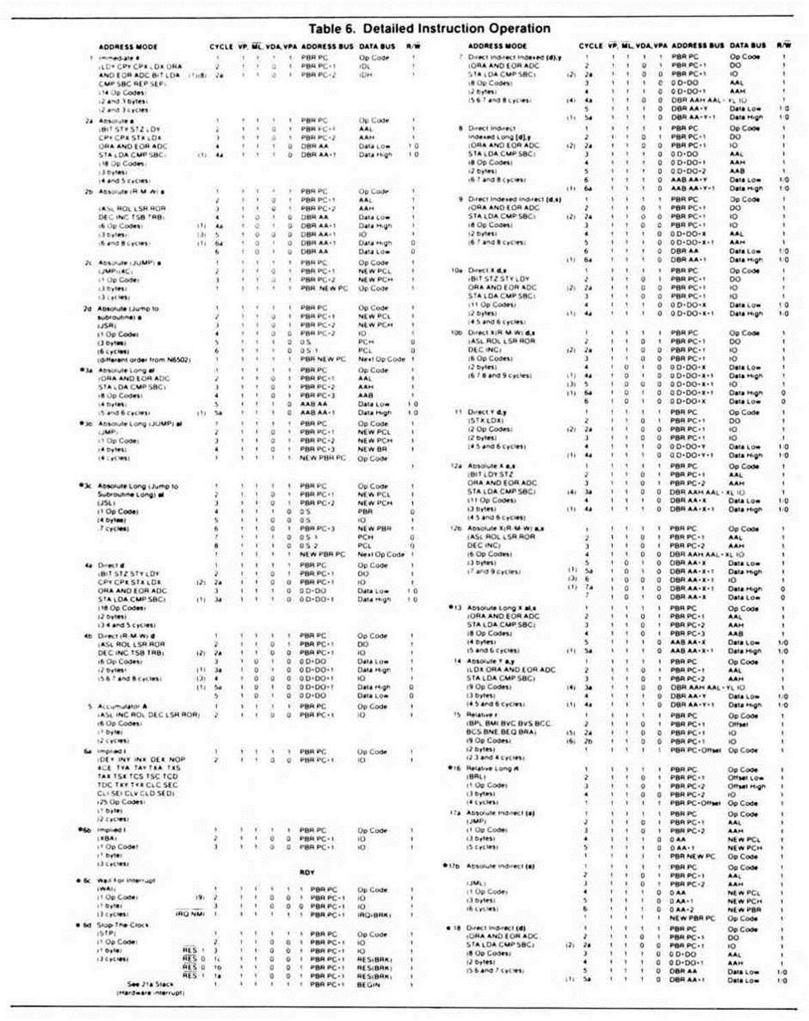
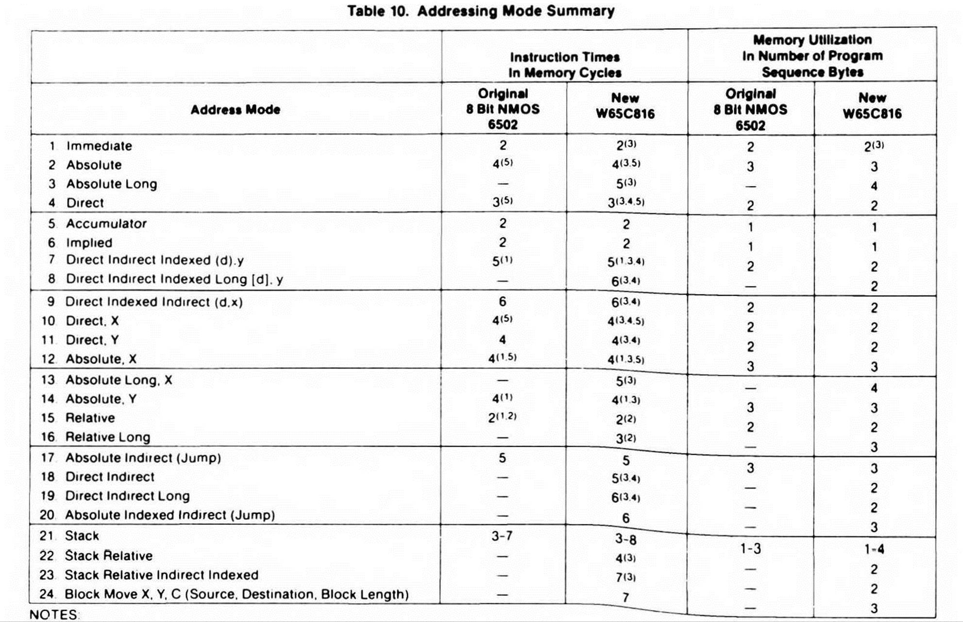
Twenty-four addressing modes are available for use with the W65C802 and W65C816 microprocessors. The "long" addressing modes may be used with the W65C802; however, the high byte of the address is not available to the hardware. Detailed descriptions of the 24 addressing modes are as follows:
1.Immediate Addressing—#
The operand is the second byte (second and third bytes when in the 16-bit mode) of the instruction.
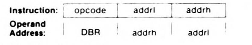
2.Absolute—a
With Absolute addressing the second and third bytes of the instruction form the low-order 16 bits of the effective address. The Data Bank Register contains the high-order 8 bits of the operand address
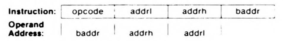
3.Absolute Long—al
The second, third, and fourth byte of the instruction form the 24-bit effective address
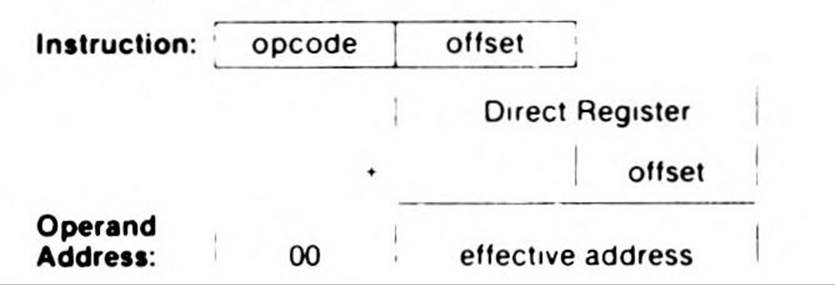
4.Direct—d
The second byte of the instruction is added to the Direct Register (D) to form the effective address An additional cycle is required when the Direct Register is not page aligned (DL not equal 0). The Bank register is always 0.
5.Accumulator—A
This form of addressing always uses a single byte instruction. The operand is the Accumulator.
6.Implied—I
Implied addressing uses a single byte instruction. The operand is implicitly defined by the instruction.
7.Direct Indirect Indexed—(d),y
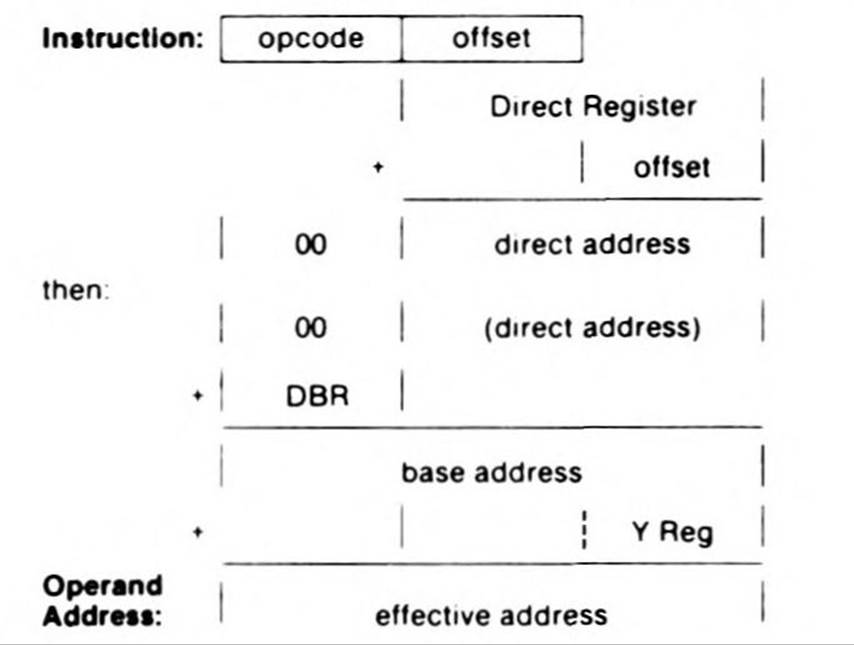
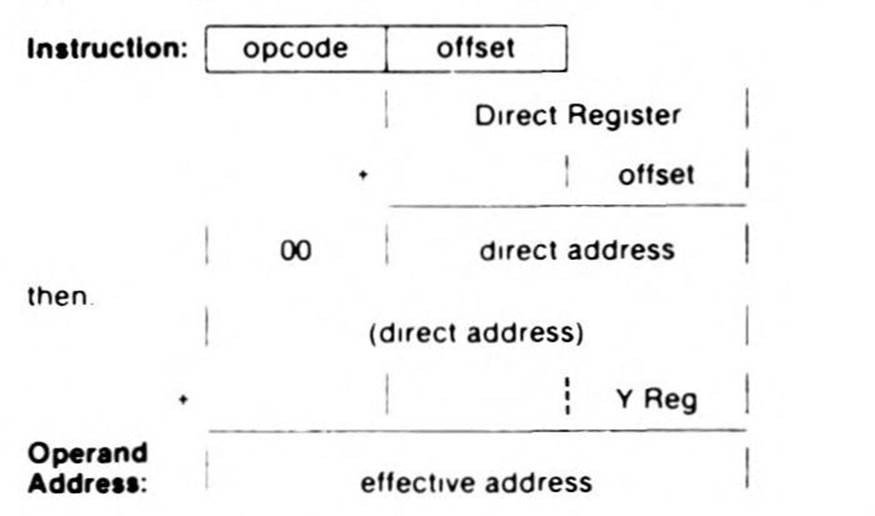
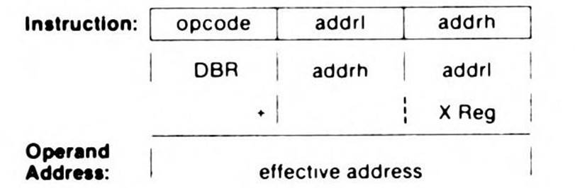
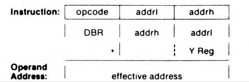
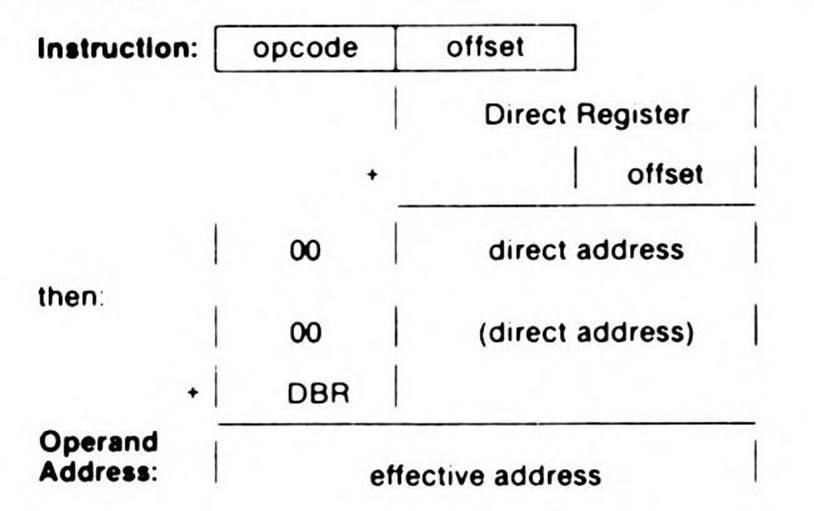
This address mode is often referred to as Indirect.Y. The second byte of the instruction is added to the Direct Register (D). The 16-bit contents of this memory location is then combined with the Data Bank register to form a 24-bit base address. The Y Index Register is added to the base address to form the effective address.
8.Direct Indirect Long Indexed—[d],y
With this addressing mode, the 24-bit base address is pointed to by the sum of the second byte of the instruction and the Direct Register. The effective address is this 24-bit base address plus the Y Index Register.
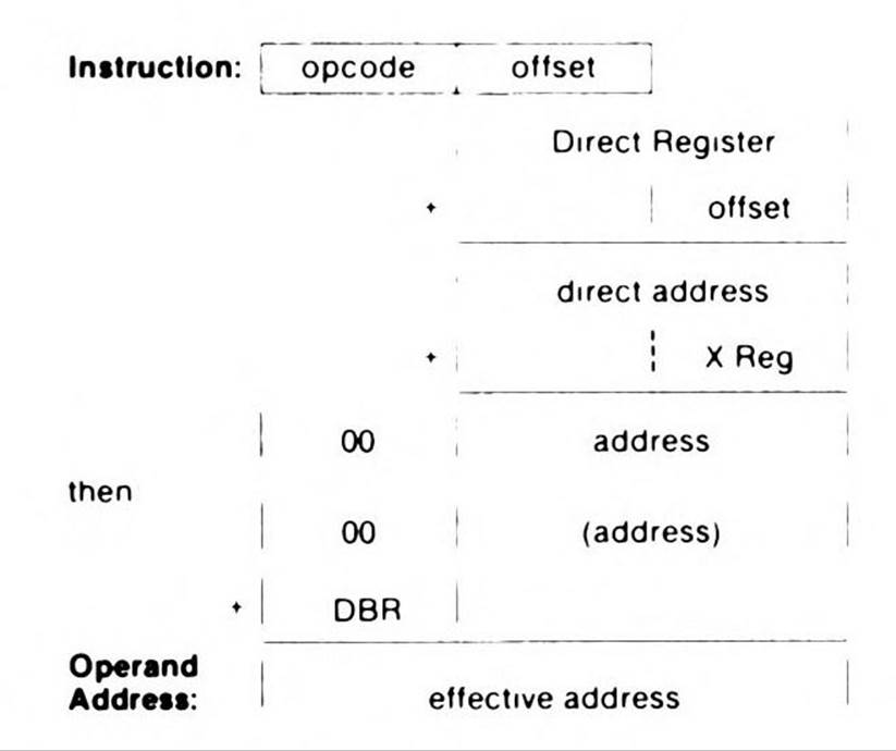
9.Direct Indexed Indirect—(d.x)
This address mode is often referred to as Indirect.X. The second byte of the instruction is added to the sum of the Direct Register and the X Index Register. The result points to the low-order 16 bits of the effective address. The Data Bank Register contains the high-order 8 bits of the effective address.
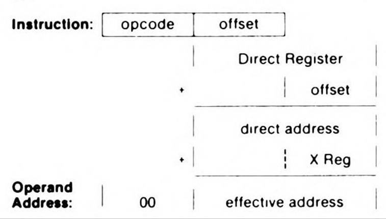
10.Direct Indexed With X—d,x
The second byte of the instruction is added to the sum of the Direct Register and the X Index Register to form the 16-bit effective address. The operand is always in Bank 0.
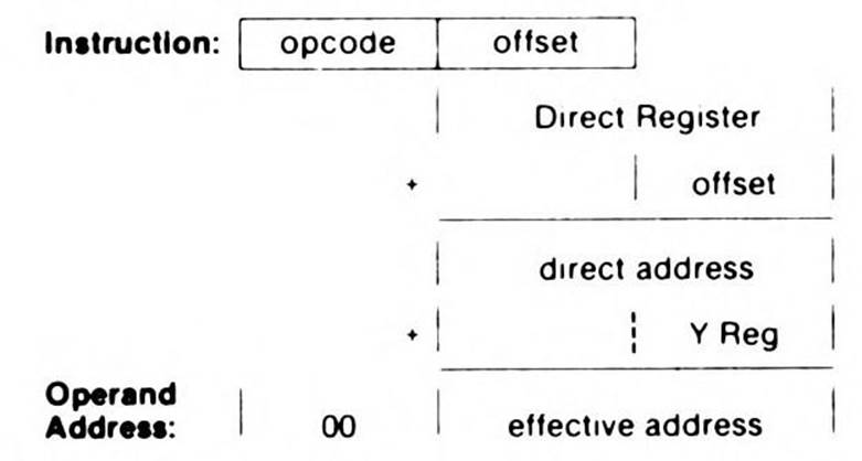
11.Direct Indexed With Y—d,y
The second byte of the instruction is added to the sum of the Direct Register and the Y Index Register to form the 16-bit effective address. The operand is always in Bank 0.
12.Absolute Indexed With X—a,x
The second and third bytes of the instruction are added to the X Index Register to form the low-order 16 bits of the effective address. The Data Bank Register contains the high-order 8 bits of the effective address.
13.Absolute Long Indexed With X—al,x
The second, third and fourth bytes of the instruction form a 24-bit base address. The effective address is the sum of this 24-bit address and the X Index Register.
14.Absolute Indexed With Y—a,y
The second and third bytes of the instruction are added to the Y Index Register to form the low-order 16 bits of the effective address. The Data Bank Register contains the high-order 8 bits of the effective address.
15.Program Counter Relative—r
This address mode, referred to as Relative Addressing, is used only with the Branch instructions. If the condition being tested is met, the second byte of the instruction is added to the Program Counter, which has been updated to point to the opcode of the next instruction. The offset is a signed 8-bit quantity in the range from -128 to 127. The Program Bank Register is not affected.
16.Program Counter Relative Long—rt
This address mode, referred to as Relative Long Addressing, is used only with the Unconditional Branch Long instruction (BRL) and the Push Effective Relative instruction (PER). The second and third bytes of the instruction are added to the Program Counter, which has been updated to point to the opcode of the next instruction. With the branch instruction, the Program Counter is loaded with the result. With the Push Effective Relative instruction, the result is stored on the stack. The offset is a signed 16-bit quantity in the range from -32768 to 32767. The Program Bank Register is not affected.
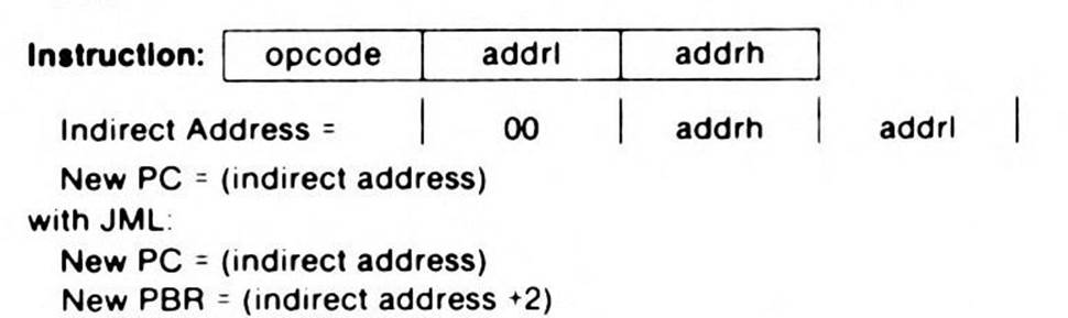
17.Absolute Indirect—(a)
The second and third bytes of the instruction form an address to a pointer in Bank 0. The Program Counter is loaded with the first and second bytes at this pointer. With the Jump Long (JML) instruction, the Program Bank Register is loaded with the third byte of the pointer.
18.Direct Indirect—(d)
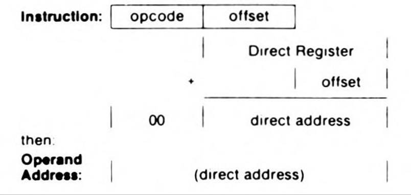
The second byte of the instruction is added to the Direct Register to form a pointer to the low-order 16 bits of the effective address. The Data Bank Register contains the high-order 8 bits of the effective address.
19.Direct Indirect Long—[d]
The second byte of the instruction is added to the Direct Register to form a pointer to the 24-bit effective address.
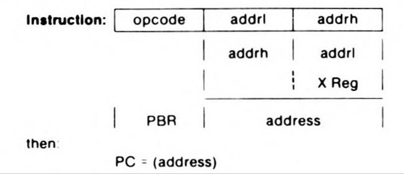
20.Absolute Indexed Indirect—(a,x)
The second and third bytes of the instruction are added to the X Index Register to form a 16-bit pointer in Bank 0. The contents of this pointer are loaded in the Program Counter. The Program Bank Register is not changed.
21.Stack—s
Stack addressing refers to all instructions that push or pull data from the stack, such as Push. Pull, Jump to Subroutine, Return from Subroutine, Interrupts, and Return from Interrupt. The bank address is always 0. Interrupt Vectors are always fetched from Bank 0
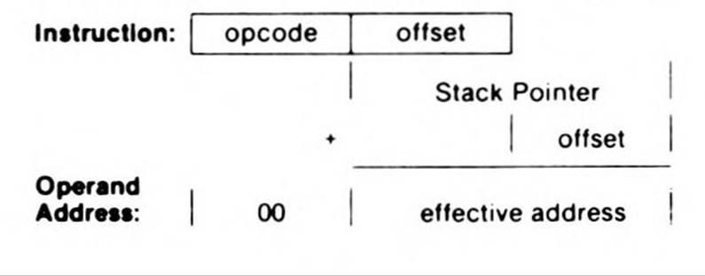
22.Stack Relative—d,s
The low-order 16 bits of the effective address is formed from the sum of the second byte of the instruction and the Stack Pointer. The high-order 8 bits of the effective address is always zero. The relative offset is an unsigned 8-bit quantity in the range of 0 to 255.
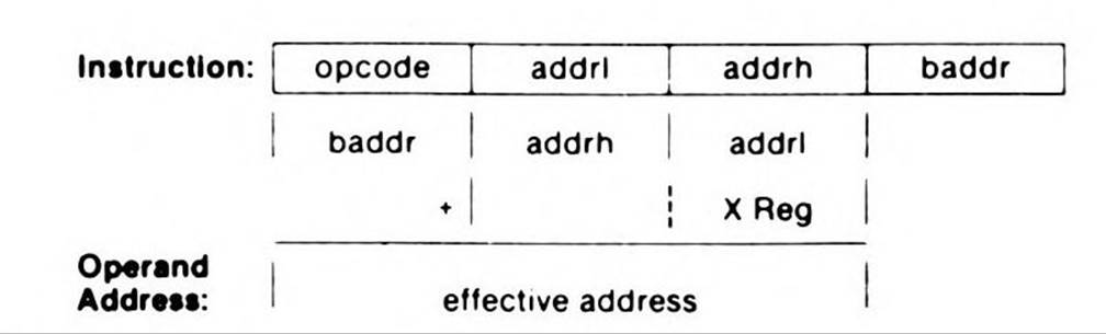
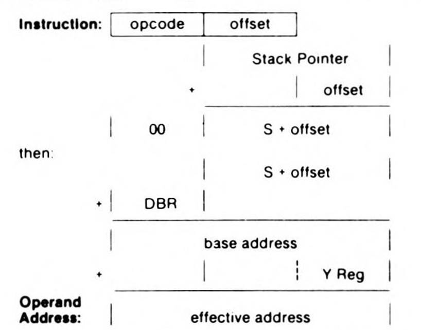
23.Stack Relative Indirect Indexed—(d,s),y
The second byte of the instruction is added to the Stack Pointer to form a pointer to the low-order 16-bit base address in Bank 0. The Data Bank Register contains the high-order 8 bits of the base address The effective address is the sum of the 24-bit base address and the Y Index Register.
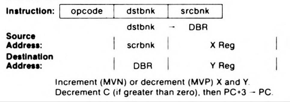
24.Block Source Bank, Destination Bank—xyc
This addressing mode is used by the Block Move instructions. The second byte of the instruction contains the high-order 8 bits of the destination address. The Y index Register contains the low-order 16 bits of the destination address. The third byte of the instruction contains the high-order 8 bits of the source address. The X Index Register contains the low-order 16 bits of the source address. The C Accumulator contains one less than the number of bytes to move. The second byte of the block move instructions is also loaded into the Data Bank Register.
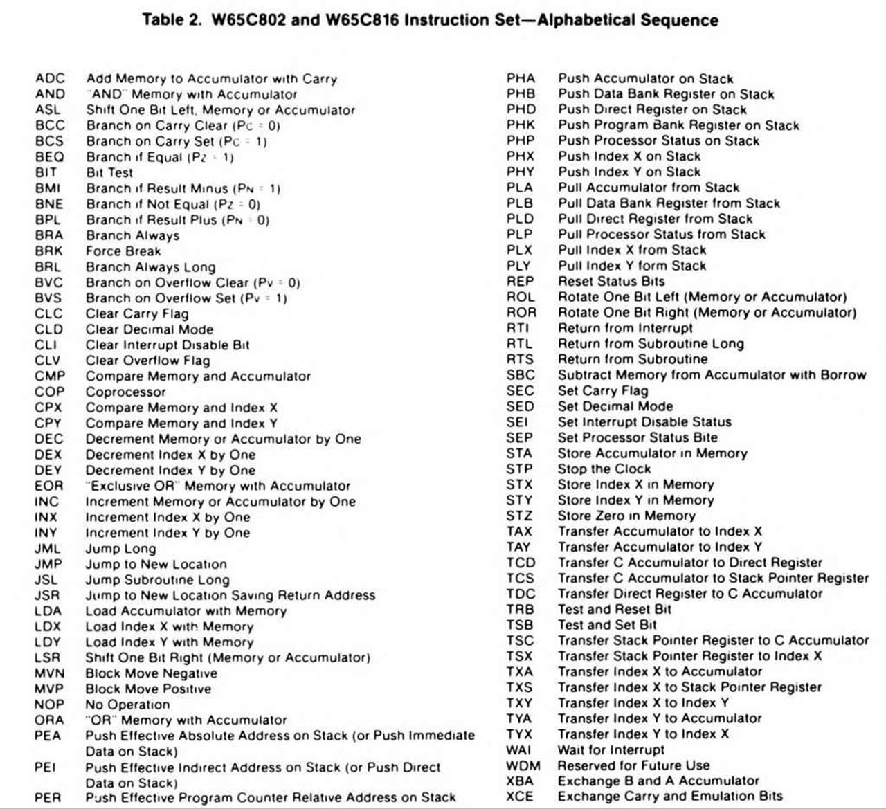
For alternate mnemonics, see Table 7.
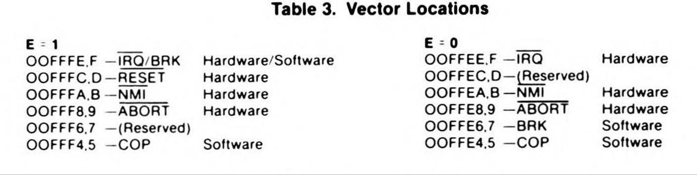
The VP output is low during the two cycles used for vector location access When an interrupt is executed, D 0 and I = 1 in Status Register P.
Opcode Matrix
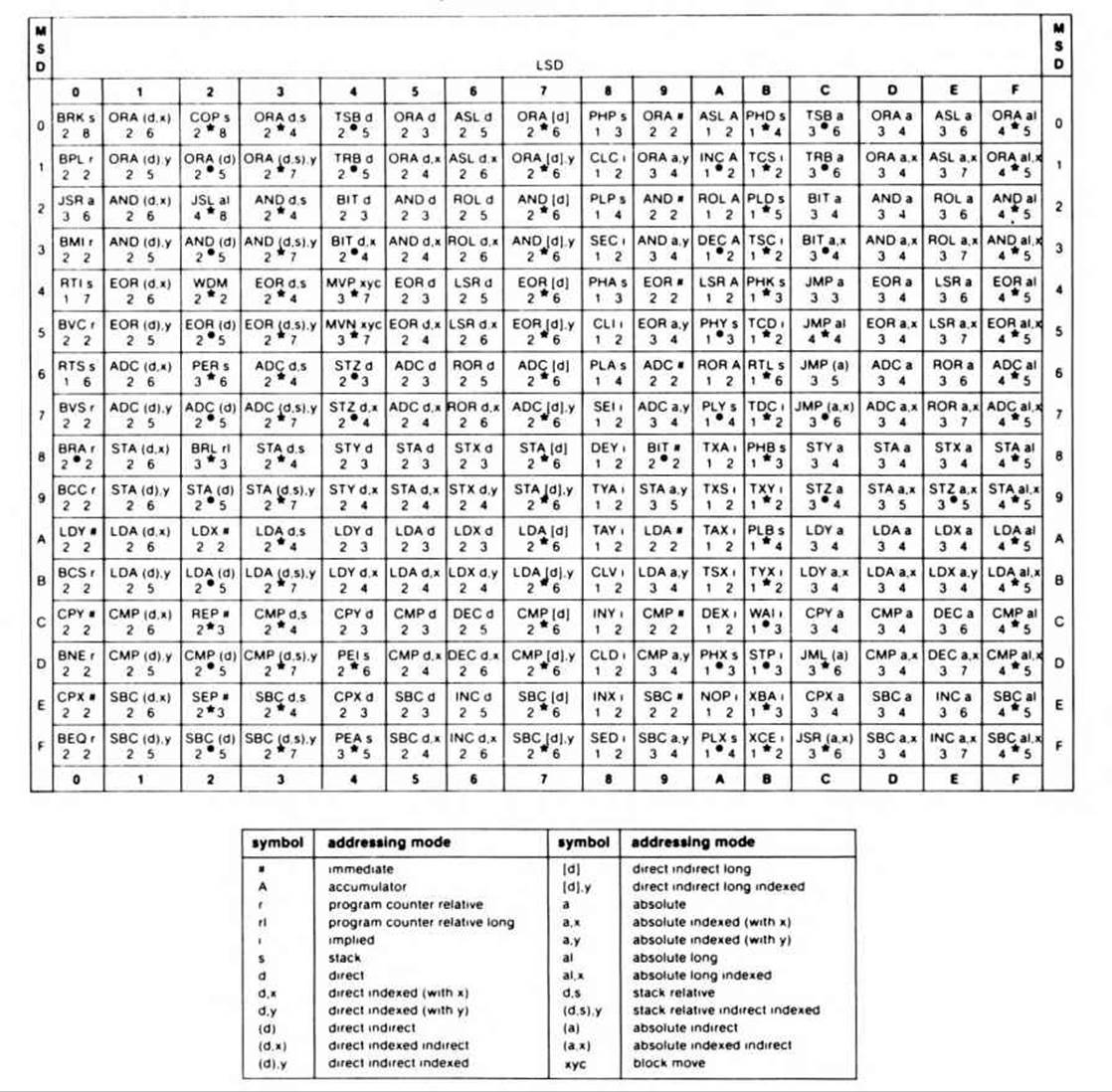
Op Code Matrix Legend
Recommended W65C816 and W65C802 Assembler Syntax Standards
Directives
Assembler directives are those parts of the assembly language source program which give directions to the assembler, this includes the definition of data area and constants within a program. This standard excludes any definitions of assembler directives.
Comments
An assembler should provide a way to use any line of the source program as a comment. The recommended way of doing this is to treat any blank line, or any line that starts with a semi-colon or an asterisk as a comment. Other special characters may be used as well.
The Source Line
Any line which causes the generation of a single W65C816 or W65C802 machine language instruction should be divided into four fields: a label field, the operation code, the operand, and the comment field.
The Label Field—The label field begins in column one of the line. A label must start with an alphabetic character, and may be followed by zero or more alphanumeric characters. An assembler may define an upper limit on the number of characters that can be in a label, so long as that upper limit is greater than or equal to six characters. An assembler may limit the alphabetic characters to upper-case characters if desired If lowercase characters are allowed, they should be treated as identical to their upper-case equivalents Other characters may be allowed in the label, so long as their use does not conflict with the coding of operand fields.
The Operation Code Field—The operation code shall consist of a three character sequence (mnemonic) from Table 3. It shall start no sooner than column 2 of the line, or one space after the label if a label is coded.
Many of the operation codes in Table 3 have duplicate mnemonics, when two or more machine language instructions have the same mnemonic; the assembler resolves the difference based on the operand.
If an assembler allows lower-case letters in labels, it must also allow lower-case letters in the mnemonic. When lower-case letters are used in the mnemonic, they shall be treated as equivalent to the upper-case counterpart. Thus, the mnemonics LDA, Ida, and LdA must all be recognized. and are equivalent.
In addition to the mnemonics shown in Table 3. an assembler may provide the alternate mnemonics shown in Table 6.
Table7. Alternate Mnemonics
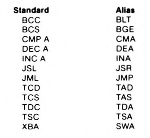
JSL should be recognized as equivalent to JSR when it is specified with a long absolute address. JML is equivalent to JMP with long addressing forced
The Operand Field—The operand field may start no sooner than one space after the operation code field. The assembler must be capable of at least twenty-four bit address calculations. The assembler should be capable of specifying addresses as labels, integer constants, and hexadecimal constants. The assembler must allow addition and subtraction in the operand field Labels. shall be recognized by the fact that they start alphabetic characters. Decimal numbers shall be recognized as containing only the decimal digits 0 9. Hexadecimal constants shall be recognized by prefixing the constant with a "$" character, followed by zero or more of either the decimal digits or the hexadecimal digits "A" "F". If lower-case letters are allowed in the label field, then they shall also be allowed as hexadecimal digits.
All constants, no matter what their format, shall provide at least enough precision to specify all values that can be represented by a twenty-four bit signed or unsigned integer represented in two's complement notation.
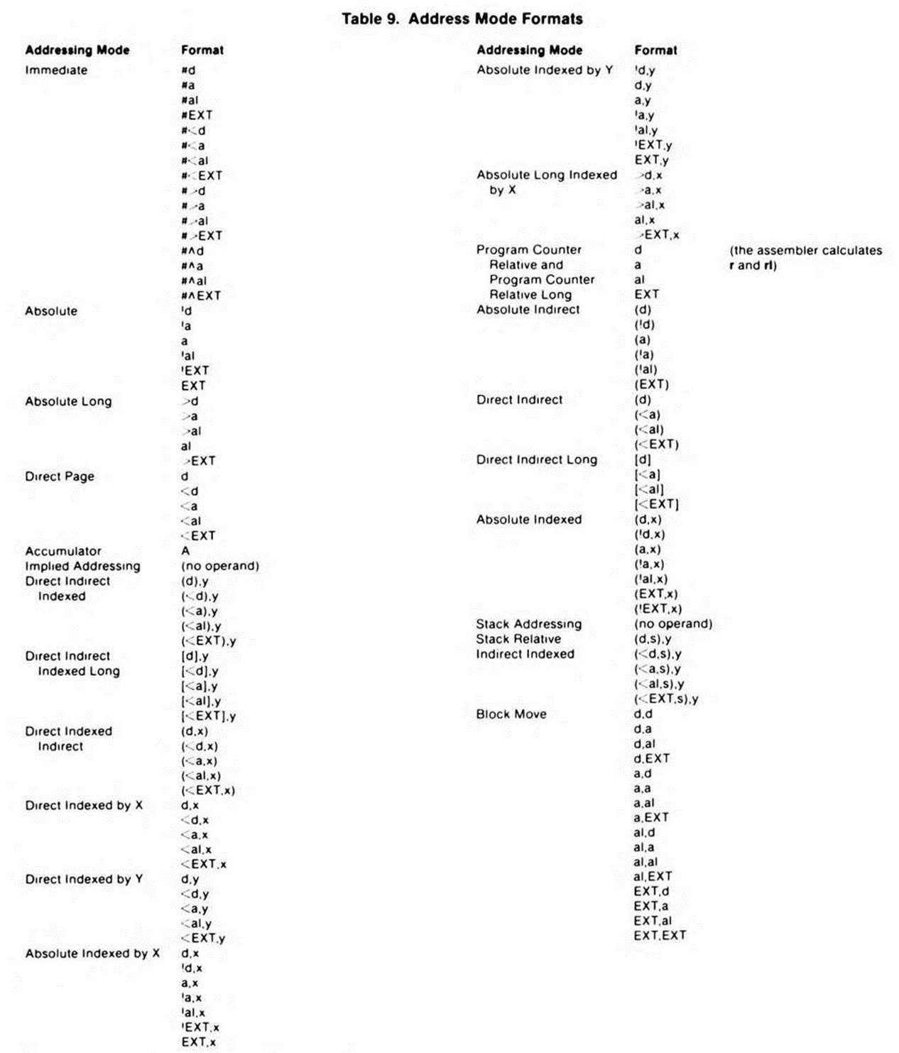
Table 8 shows the operand formats which shall be recognized by the assembler. The symbol d is a label or value which the assembler can recognize as being less than $100. The symbol a is a label or value which the assembler can recognize as greater the $FF but less than $10000; the symbol al is a label of value that the assembler can recognize as being greater than $FFFF. The symbol EXT is a label which cannot be located by the assembler at the time the instruction is assembled Unless in-structed otherwise, an assembler shall assume that EXT labels are two bytes long. The symbols r and rl are 8 and 16 bit signed displacements calculated by the assembler.
Note that the operand does not determine whether or not immediate addressing loads one or two bytes; this is determined by the setting of the status register. This forces the requirement for a directive or directives that tell the assembler to generate one or two bytes of space for immediate loads. The directives provided shall allow separate settings for the accumulator and index registers.
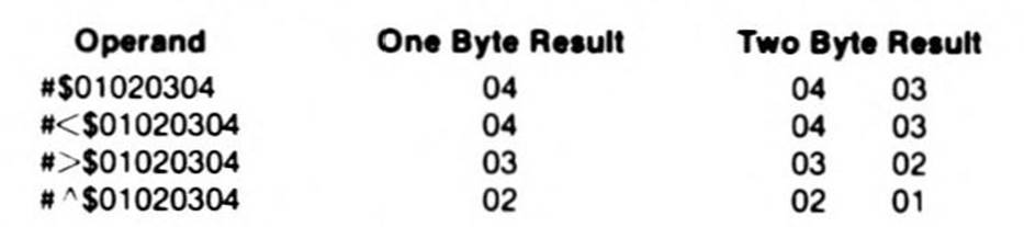
The assembler shall use the < . >. and ∧ characters after the # character in immediate address to specify which byte or bytes will be selected from the value of the operand. Any calculations in the operand must be performed before the byte selection takes place Table 7 defines the action taken by each operand by showing the effect of the operator on an address. The column that shows a two byte immediate value show the bytes in the order in which they appear in memory. The coding of the operand is for an assembler which uses 32 bit address calculations, showing the way that the address should be reduced to a 24 bit value.
Table 8 . Byte Selection Operator
In any location in an operand where an address, or expression resulting in an address, can be coded, the assembler shall recognize the prefix characters < .|. and > . which force one byte (direct page), two byte (absolute) or three byte (long absolute) addressing. In cases where the addressing mode is not forced, the assembler shall assume that the address is two bytes unless the assembler is able to determine the type of addressing required by context, in which case that addressing mode will be used. Addresses shall be truncated without error if an addressing mode is forced which does not require the entire value of the address For example.

are completely equivalent. If the addressing mode is not forced, and the type of addressing cannot be determined from context, the assembler shall assume that a two byte address is to be used. If an instruction does not have a short addressing mode (as in LDA, which has no direct page indexed by Y) and a short address is used in the operand, the assembler shall automatically extend the address by padding the most significant bytes with zeroes in order to extend the address to the length needed. As with immediate addressing, any expression evaluation shall take place before the address is selected, thus, the address selection character is only used once, before the address of expression.
The! (exclamation point) character should be supported as an alternative to the | (vertical bar).
A long indirect address is indicated in the operand field of an instruction by surrounding the direct page address where the indirect address is found by square brackets, direct page addresses which contain sixteen-bit addresses are indicated by being surrounded by parentheses.
The operands of a block move instruction are specified as source bank, destination bank—the opposite order of the object bytes generated.
Comment Field—The comment field may start no sooner than one space after the operation code field or operand field depending on instruction type.
Note The alternate ! (exclamation point) is used in place of the | (vertical bar).
NOTES:
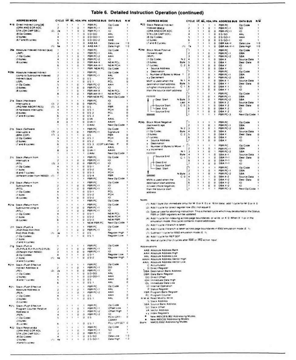
1 Page boundary, add 1 cycle if page boundary is crossed when forming address.
2 Branch taken, add 1 cycle if branch is taken.
3 M = 0 or X = 0.16 bit operation, add 1 cycle, add 1 byte for immediate.
4 Direct register low (DL) not equal zero, add 1 cycle.
5 Read-Modify-Write, add 2 cycles for M = 1, add 3 cycles for M = 0.
Caveats and Application Information Stack Addressing
When in the Native mode, the Stack may use memory locations 000000 to 00FFFFF. The effective address of Stack. Stack Relative, and Stack Relative Indirect Indexed addressing modes will always be within this range. In the Emulation mode, the Stack address range is 000100 to 0001FF. The following opcodes and addressing modes will increment or decrement beyond this range when accessing two or three bytes.
JSL: JSR(a,x): PEA; PEI; PER; PHD; PLD; RTL; d.s. (d.s).y
Direct Addressing
The Direct Addressing modes are often used to access memory registers and pointers. The effective address generated by Direct. Direct.X and Direct.Y addressing modes will always be in the Native mode range 000000 to OOFFFF. When in the Emulation mode, the direct addressing range is 000000 to 0000FF, except for [Direct] and [Directj.Y addressing modes and the PEI instruction which will increment from 0000FE or OOOOFF into the Stack area.
When in the Emulation mode and DH is not equal to zero, the direct addressing range is 00DH00toOODHFF. except for [Direct] and [Directj.Y addressing modes and the PEI instruction which will increment from OODHFE or OODHFF into the next higher page.
When in the Emulation mode and DL in not equal to zero, the direct addressing range is 000000 to OOFFFF.
Absolute Indexed Addressing (W65C816 Only)
The Absolute Indexed addressing modes are used to address data outside the direct addressing range. The W65C02 and W65C802 addressing range is 0000 to FFFF. Indexing from page FFXX may result in a 00YY data fetch when using the W65C02 or W65C802. In contrast, indexing from page ZZFFXX may result in ZZ+1 .OOYY when using the W65C816.
Future Microprocessors (i.e., W65C832)
Future WDC microprocessors will support all current W65C816 operating modes for both index and offset address generation.
ABORT Input (W65C816 Only)
ABORT should be held low for a period not to exceed one cycle. Also, if ABORT is held low during the Abort Interrupt sequence, the Abort Interrupt wiM be aborted. It is not recommended to abort the Abort Interrupt. The ABORT internal latch is cleared during the second cycle of the Abort Interrupt Asserting the ABORT input after the following instruction cycles will cause registers to be modified:
•Read-Modify-Write: Processor status modified if ABORT is asserted after a modify cycle.
•RTI: Processor status will be modified if ABORT is asserted after cycle 3.
• IRQ, NMI, ABORT BRK, COP: When ABORT is asserted after cycle 2, PBR and DBR will become 00 (Emulation mode) or PBR will become 00 (Native mode).
The Abort Interrupt has been designed for virtual memory systems. For this reason, asynchronous ABORT'S may cause undesirable results due to the above conditions.
VDA and VPA Valid Memory Address Output Signals (W65C816 Only)
When VDA or VPA are high and during all write cycles, the Address Bus is always valid. VDA and VPA should be used to qualify all memory cycles. Note that when VDA and VPA are both low. invalid addresses may be generated. The Page and Bank addresses could also be invalid. This will be due to low byte addition only. The cycle when only low byte addition occurs is an optional cycle for instructions which read memory when the Index Register consists of 8 bits. This optional cycle becomes a standard cycle for the Store instruction, all instructions using the 16-bit Index Register mode, and the Read-Modify-Write instruction when using 8-or 16-bit Index Register modes.
Apple II, lle, lle and ll+ Disk Systems (W65C816 Only)
VDA and VPA should not be used to qualify addresses during disk operation on Apple systems. Consult your Apple representative for hardware/software configurations.
DB/BA Operation when RDY is Pulled Low (W65C816 Only)
When RDY is low. the Data Bus is held in the data transfer state (i.e., Φ2high) The Bank address external transparent latch should be latched when the Φ2 clock or RDY is low.
M/X Output (W65C816 Only)
The M/X output reflects the value of the M and X bits of the processor Status Register. The REP. SEP and PLP instructions may change the state of the M and X bits. Note that the M/X output is invalid during the instruction cycle following REP, SEP and PLP instruction execution. This cycle is used as the opcode fetch cycle of the next instruction.
All Opcodes Function in All Modes of Operation
It should be noted that all opcodes function in all modes of operation. However, some instructions and addressing modes are intended for W65C816 24-bit addressing and are therefore less useful for the W65C802. The following is a list of instructions and addressing modes which are primarily intended for W65C816 use:
JSL; RTL; [d ]; [d].y. JMP al; JML; al; al,x
The following instructions may be used with the W65C802 even though a Bank Address is not multiplexed on the Data Bus:
PHK; PHB; PLB
The following instructions have "limited" use in the Emulation mode:
•The REP and SEP instructions cannot m odify the M and X bits when in the Emulation mode. In this mode the M and X bits will always be high (logic 1).
•When in the Emulation mode, the MVP and MVN instructions use the X and Y Index Registers for the memory address. Also, the MVP and MVN instructions can only move data within the memory range 0000 (Source Bank) to 00FF (Destination Bank) for the W65C816, and 0000 to 00FF for the W65C802
Indirect Jumps
The JMP (a) and JML (a) instructions use the direct Bank for indirect addressing, while JMP (a.x) and JSR (a.x) use the Program Bank for indirect address tables.
Switching Modes
When switching from the Native mode to the Emulation mode, the X and M bits of the Status Register are set high (logic 1), the high byte of the Stack is set to 01. and the high bytes of the X and Y Index Registers are set to 00. To save previous values, these bytes must always be stored before changing modes. Note that the low byte of the S. X and Y Registers and the low and high byte of the Accumulator (A and B) are not affected by a mode change.
How Hardware Interrupts, BRK, and COP Instructions Affect the Program Bank and the Data Bank Registers
When in the Native mode, the Program Bank register (PBR) is cleared to 00 when a hardware interrupt, BRK or COP is executed. In the Native mode, previous PBR contents is automatically saved on Stack.
In the Emulation mode, the PBR and DBR registers are cleared to 00 when a hardware interrupt. BRK or COP is executed. In this case, previous contents of the PBR are not automatically saved.
Note that a Return from Interrupt (RTI) should always be executed from the same "mode" which originally generated the interrupt.
Binary Mode
The Binary mode is set whenever a hardware or software interrupt is executed The D flag within the Status Register is cleared to zero.
WAI Instruction
The WAI instruction pulls RDY low and places the processor in the WAI "low power" mode NMI. IRQ or RESET will terminate the WAI condition and transfer control to the interrupt handler routine. Note that an ABORT input will abort the WAI instruction, but will not restart the processor. When the Status Register I flag is set (IRQ disabled), the IRQ interrupt will cause the next instruction (following the WAI instruction) to be executed without going to the IRQ interrupt handler. This method results in the highest speed response to an IRQ input. When an interrupt is received after an ABORT which occurs during the WAI instruction, the processor will return to the WAI instruction Other than RES (highest priority). ABORT is the next highest priority, followed by NMI or IRQinterrupts.
STP Instruction
The STP instruction disables the Φ2 clock to all circuitry. When disabled, the Φ2 clock is held in the high state In this case, the Data Bus will remain in the data transfer state and the Bank address will not be multiplexed onto the Data Bus. Upon executing the STP instruction, the RES signal is the only input which can restart the processor. The processor is restarted by enabling the Φ2 clock, which occurs on the falling edge of the RES input Note that the external oscilla tor must be stable and operating properly before RES goes high.
COP Signatures
Signatures 00-7F may be user defined, while signatures 80-FF are reserved for instructions on future microprocessors (i.e.. W65C832). Contact WDC for software emulation of future microprocessor hardware functions.
WDM Opcode Use
The WDM opcode will be used on future microprocessors For example, the new W65C832 uses this opcode to provide 32-bit floating-po int and other 32-bit math and data operations Note that the W65C832 will be a plug-to-plug replacement for the W65C816. and can be used where high-speed. 32-bit math processing is required The W65C832 will be available in the near future.
RDY Pulled During Write
The NMOS 6502 does not stop during a write operation. In contrast, both the W65C02 and the W65C816 do stop during write operations. The W65C802 stops during a write when in the Native mode, but does not stop when in the Emulation mode.
MVN and MVP Affects on the Data Bank Register
The MVN and MVP instructions change the Data Bank Register to the value of the second byte of the instruction (destination bank address).
Interrupt Priorities
The following interrupt priorities will be in effect should more than one interrupt occur at the same time.
Transfers from 8-Bit to 16-Bit, or 16-Bit to 8-Bit Registers
All transfers from one register to another will result in a full 16-bit output from the source register. The destination register size will determine the number of bits actually stored in the destination register and the values stored in the processor Status Register. The following are always 16-bit transfers, regardless of the accumulator size:
TCS; TSC; TCD; TDC
Stack Transfers
When in the Emulation mode, a 01 is forced into SH In this case, the B Accumulator will not be loaded mtoSH during a TCS instruction. When in the Native mode, the B Accumulator is transferred to SH Note that in both the Emulation and Native modes, the full 16 bits of the Stack Register are transferred to the A, B and C Accumulators, regardless of the state of the M bit in the Status Register.
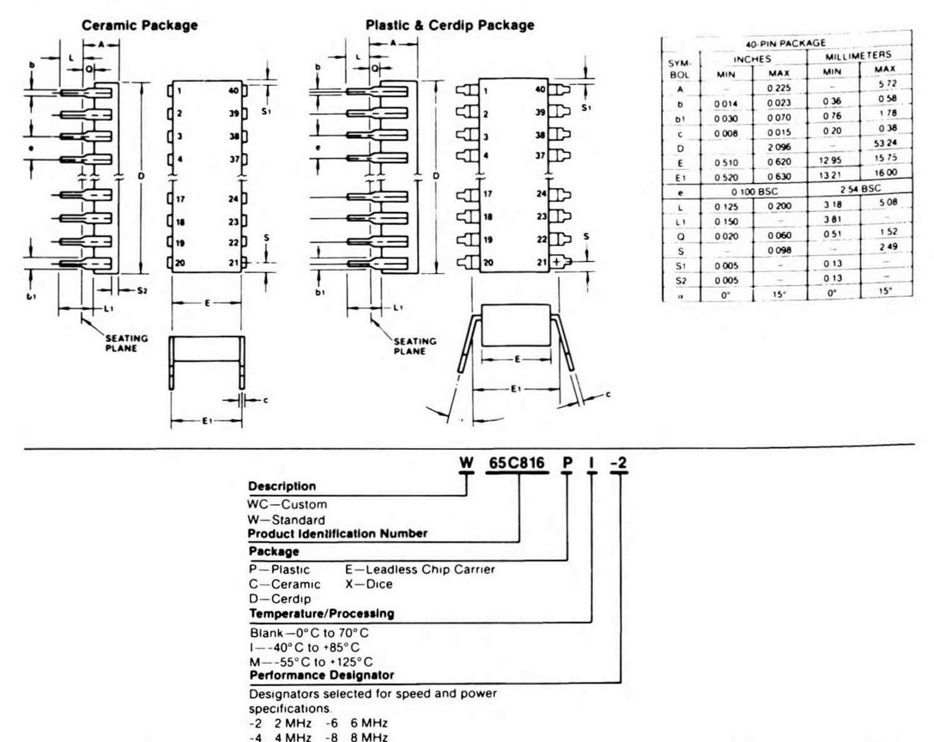
Packaging Information
Sales Offices:
Technical or sales assistance may be requested from:
The Western Design Center, Inc.
2166 East Brown Road
Mesa. Arizona 85203
602/962-4545
TLX 6835057
WDC reserves the right to make changes at any time and without notice
Information contain ed herein is provided gratuitously and without liability, to any user Reasonable efforts have been made to verify the accuracy of the information but no guarantee whatsoever is given as to the accuracy or as to its applicability to particular uses. In every instance it must be the responsibility of the user to determine the suitability of the products for each application WDC products are not authorized for use as critical components in life support devices or systems No thing contained herein shall be construed as a recommendation to use any product in violation of existing patents or other rights of third parties The sale of any WDC product is subject to a ll WDC Terms and Conditions of Sale and Sales Policies copies of which are available upon request
•The Western Design Center Inc 1985

All materials on the site are licensed Creative Commons Attribution-Sharealike 3.0 Unported CC BY-SA 3.0 & GNU Free Documentation License (GFDL)
If you are the copyright holder of any material contained on our site and intend to remove it, please contact our site administrator for approval.
© 2016-2026 All site design rights belong to S.Y.A.