Make: More Electronics (2014)
Chapter 27. Experiment 27: Shifting Bits
A counter with decoded outputs can be used for entertainment in games and flashing-light displays, but perhaps you don’t always want single LEDs to flash in sequence. Perhaps you want to create a sequence of your own.
The component that will do this for you is known as a shift register. Very interesting, but—why is this interesting? What would you use it for?
I can provide some practical answers to these questions, but first I’d like you to set up a circuit that you’ll need to trigger the shift register and control other experiments in the future. It provides a clean pulse of a fixed length, in much the same way as the one-shot 7555 timer in the previous experiment (see Figure 26-8).
No Bouncing!
I talked about switch bounce, also known as contact bounce, in Make: Electronics. This is the nasty habit of mechanical switch contacts that vibrate for a very brief moment when they open or close. Because digital chips are so sensitive and can respond so quickly, they misinterpret vibrating contacts as multiple presses of the switch.
Switch bounce hasn’t been a problem in most of our experiments because I haven’t been using a switch or a pushbutton to send pulses to a chip that counts them. In Figure 26-1, for instance, a timer running in astable mode controlled the counters.
To test a shift register, which is going to be the subject of this experiment, you really need to advance it manually, and a bounceless switch is the only sensible way to do this.
Specifics
In my previous book, I showed that when two NOR gates or two NAND gates are wired as a flip-flop, they can debounce an input. But I prefer to use a timer for this task, as the timer can provide a pulse that has a fixed duration. This in itself can also be useful.
Figure 27-1 shows the circuit. A double-throw pushbutton must be used, because in its normal “up” position, it maintains a positive charge on the 0.033µF coupling capacitor. Meanwhile, Pin 2, the input pin of the timer, is also maintained in a high state through a 10K pullup resistor. So long as the input pin is high, nothing happens.
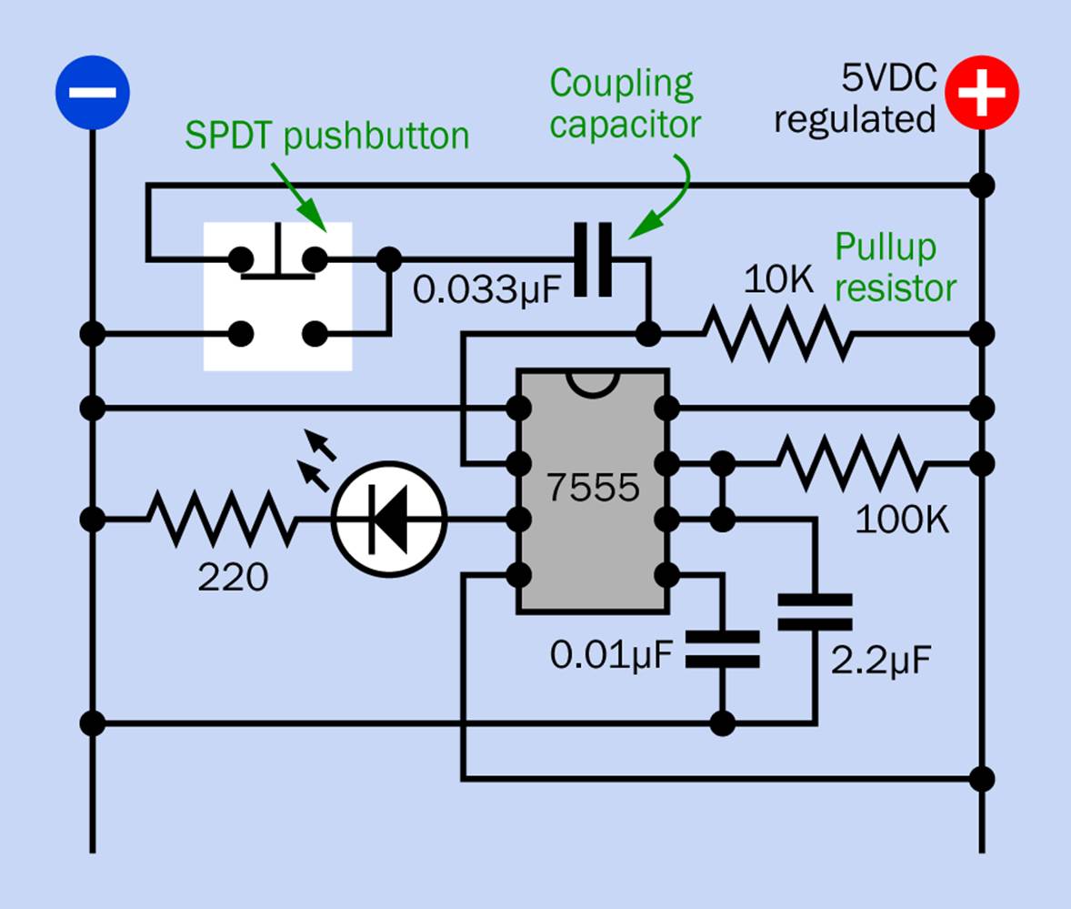
Figure 27-1. A basic circuit to deliver a clean pulse of fixed length, suppressing contact bounce that tends to be created by a pushbutton.
When the pushbutton is pressed, it grounds the coupling capacitor. This event is transmitted to the input pin of the timer, pulling it down for long enough to trigger the timer in its one-shot mode. The 100K timing resistor and 2.2µF timing capacitor deliver a pulse lasting about a quarter of a second. While this is going on, any vibration from the switch contacts is ignored.
§ The output from the timer must last longer than the contact bounce. However, the contacts stop vibrating within a couple of milliseconds.
When the timer finishes its pulse, it would normally be retriggered if its input pin was still low. In this circuit, however, even if the button is still being pressed, the coupling capacitor now blocks the DC connection, while the pullup resistor holds the timer input pin high.
§ If the pushbutton is still being held down when the output from the timer ends, the timer ignores the pushbutton, completes its cycle, and its output pulse ends.
Now suppose the pushbutton is released before the end of the timing interval. The capacitor is immediately recharged, and the pullup resistor holds the timer input high.
§ If the pushbutton is released before the output from the timer ends, the timer still completes its cycle, and its output pulse ends.
The only possibility for error is if the pushbutton is released at virtually the same moment that the timer pulse ends. Under these circumstances, if the switch contacts vibrate as they open, it is possible for retriggering to occur.
§ The timer should deliver a short pulse (a quarter second or less) or a relatively long one (one second or more) to avoid conflict if the switch contacts open and vibrate at the same moment as the timer pulse ends.
The timer is shown in the schematic with an LED attached to its output for demonstration purposes. Depending on the application, another coupling capacitor may be placed on the output from the timer to transmit a brief pulse to the next stage in the circuit, while blocking DC.
A Bit-Shifting Demo
Now we’re ready for the shift register. The setup in Figure 27-2 bears some resemblance to the ring-counter test schematic in Figure 26-1, except that it is now manually controlled with the debounced circuit that I just described. Note that it still uses a 7555 timer instead of an old-style 555.
A photograph of the breadboarded version is in Figure 27-3.
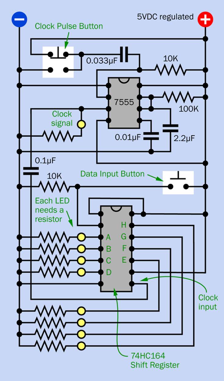
Figure 27-2. A test circuit that shows how a shift register moves the contents of its memory locations in response to a clock signal. The pushbutton loads data into the shift register.
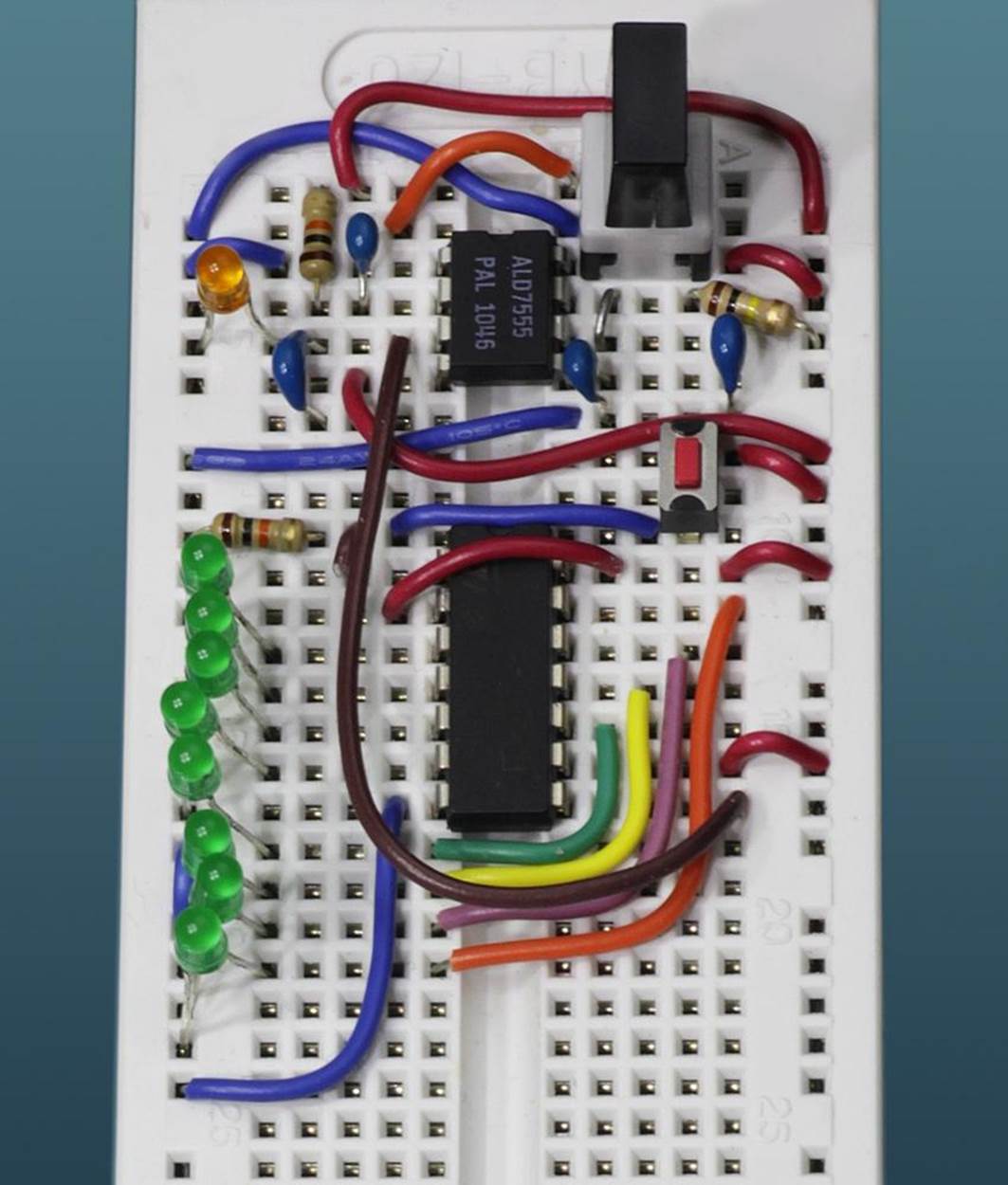
Figure 27-3. The breadboarded version of the shift-register test circuit.
While the pin values of the ring counter that you used previously (and the decoder before that) were not in numerical sequence, the outputs from the 74HC164 shift register are much more convenient, proceeding sequentially from pin 3 around the chip, counterclockwise. This makes it easy to attach a vertical line of LEDs that will light up in sequence, although the sequence will be from the top down instead of bottom-up.
As before, the yellow circles in Figure 27-2 represent LEDs. If your LEDs do not contain their own resistors, you will need one resistor for each and every LED in this circuit. While the decoder and the ring counter lit only one LED at a time, the shift register can illuminate any combination, including all eight simultaneously.
I added a “clock signal” LED just to show that the output from the timer is alive and well, because when you apply power to this circuit, the eight output LEDs are likely to do nothing. This is because the memory locations in the shift register are empty until you put some data into them.
Hold down the Data Input button. While you are holding it down, press the Clock Pulse button repeatedly. The Data Input button applies a high state to the input buffer of the shift register, and each time you press the Clock Pulse button, the state of the input buffer is copied into the first memory location of the shift register (identified as “A” in the schematic) while the contents of the other memory locations are bumped along to make room.
Now let go of the Data Input button, and the 10K pulldown resistor applies a low state to the input buffer. If you continue to press the Clock Pulse button, low states are “clocked in” to the shift register, and as before, the memory contents are moved along to make room. What happens to the last one, identified as “H” in the schematic? It is discarded.
A single shift cycle of the register is represented in Figure 27-4. Each of the eight memory locations can be thought of as containing a binary digit, or bit. In this diagram, initially the bits in locations C and H happen to be high. First, the pushbutton inserts a high state into the input buffer. Second, a rising clock pulse causes the shift register to move all the bits along and copy the high state in the input buffer into location A.
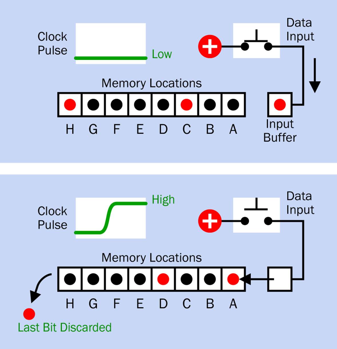
Figure 27-4. Data moving into and through a shift register.
The tactile switch in the schematic is not debounced because the shift register only checks its state at the moment when the clock pulse rises from low to high. The rest of the time, the shift register ignores the tactile switch—and in fact, if you press it briefly between clock pulses, the shift register will not notice.
Quick Facts About Shift Registers
§ The shift register contains memory locations, each of which holds a high state or a low state. You can think of them as binary digits.
§ Most shift registers are eight-bit components. However, it is possible to chain several of them together.
§ A signal on the clock pin of the shift register tells it to throw away the value of the last memory location, move all the preceding bits one step along, and load a new value into the first memory location.
§ The new value is determined by the high or low state of an input pin at the beginning of a new clock cycle. Most shift registers respond to the rising edge of a clock pulse.
§ The shift register ignores the state of its input pin until it is triggered by a clock transition.
§ Some shift registers can convert parallel to serial data instead of, or as well as, serial to parallel data.
§ There is a shift register with part number TPIC6A595 that has “power logic” outputs capable of delivering 100mA or more. This can be useful in some applications.
Pinouts
Pinouts of the 74HC164 are shown in Figure 27-5. Eight pins connect with memory locations inside the chip. I’ve labelled them A through H, although some datasheets may identify them as 1A through 1H, or QA through QH, or something similar.
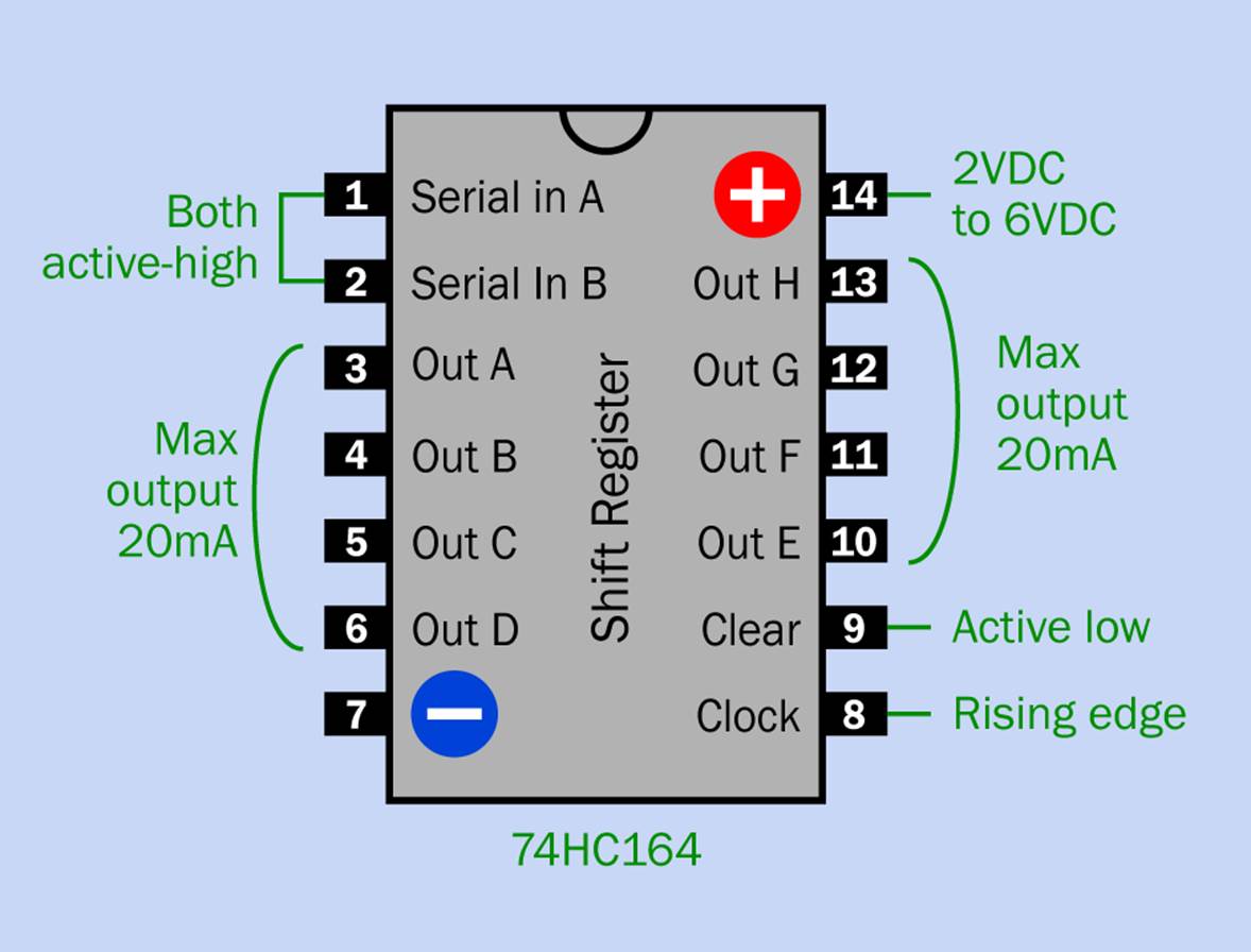
Figure 27-5. Pinouts of the 74HC164 shift register.
The Clear input is active low, and will zero out all the memory locations. Therefore, it is normally held in a high state. The chip has two serial data inputs, on pins 1 and 2. For our purposes, one input is kept high while the other receives data. The functions of pins 1 and 2 are interchangeable.
The 74HC164 is a relatively simple chip with only 14 pins. Other shift registers have additional features. I won’t be discussing those chips here.
Background: Bit Streams
Long, long ago, communication between computing devices used to be done through a serial cable, which contained three wires. One of them was negative ground, another signalled an external device to start and stop the data stream, and the third wire carried data.
When the device on the receiving end accumulated seven binary digits, it assembled them to form a binary value from 0000000 through 1111111 (0 through 127 decimal), and each of these values was interpreted as a code that could represent a letter of the alphabet in upper- or lowercase. You also had a few control codes, such as “start a new line of text.” (Subsequently the code system was extended to use eight bits, but the meaning of the additional codes was not standardized.)
This is how text was transmitted, back in the day. The character-coding system that was used for this very basic system was called ASCII, which is an acronym for American Standard Code for Information Interchange.
It was slow and primitive—yet today we still use serial data transmission, meaning that bits of data travel down a single wire, one at a time. This is true of a USB device or a SATA connection for an internal hard drive. The speeds have increased tremendously, but basic principles remain the same.
The ASCII codes are still the same, too, although they have become a subset of “Unicode,” which permits up to 32 bits per character, facilitating the inclusion of foreign languages such as Japanese.
The tricky part, which I skipped over in my explanation, is how a device on the receiving end of a serial stream “assembles” the data. The early computers could process eight bits (one byte) at a time. Therefore, they had to receive eight bits serially, shift them into eight memory locations, and then spit them out simultaneously along eight parallel wires for processing.
As I’m sure you’ve guessed, the chip that did this was the shift register. It was a register that could shift bits along. It also functioned as a serial-to-parallel converter.
Modern Applications
Today, the capability of a shift register is built into bigger chips that do other things. Still, the old chips have their uses.
For instance, suppose you want to switch eight devices on and off from a microcontroller, but you don’t have eight output pins to spare. You send eight on-or-off states over a single wire to a shift register, at high speed, using an additional wire for the clock signal that tells the shift register when each bit is coming so that it can be clocked in. The states of the eight output pins of the shift register can control the eight devices, and you can update the register so quickly, the result will seem to be instant.
Moreover, you can chain shift registers to control sixteen devices—or twenty-four, or thirty-two—and you still only need one wire to send the data. This is a very powerful concept.
Here’s a thought. Suppose we use seven bits in a shift register to represent a binary number. If we shift all the digits one space to the left, and replace the rightmost digit with a 0, we just multiplied the original value by two. Why is that? Because when you move one step left through a binary number, each binary place value is twice the one that preceded it.
Hmm . . . do you think you could adapt the binary adder that you built to do multiplication sums? It’s an intriguing idea—but I’m not going to mess with it. I’m going to use a shift register (three of them, actually) in a device that will tell your fortune.