Make: More Electronics (2014)
Chapter 25. Experiment 25: Enhancing Your Adder
Adding a decimal output to your adder is an easier task than adding a decimal input, so I’ll deal with the output first.
Return of the Decoder
It would be nice to have a couple of seven-segment numeric displays for the output, but they require drivers that use binary-coded decimal (BCD) inputs. In other words, the input to each driver must range from 0000 through 1001 binary (0 through 9 decimal). Your adder has an output ranging from 0000 through 1110 binary, and converting that to run a pair of seven-segment numerals is not so easy.
Therefore, I’ll assume you can be happy with individual LEDs, each of which will represent a decimal value.
To take care of this, we can use the 4-to-16 decoder that you first encountered in Experiment 19, although it will have to be the HC version, 74HC4514, not the old 4514 CMOS version, because each of its output pins must be capable of driving an LED. The binary inputs to the chip will be supplied by the four outputs from your adder, weighted 1, 2, 4, and 8. Output pins from the chip will drive LEDs that are assigned values 0 through 14 decimal (bearing in mind that the largest addition sum your adder will handle is 111 + 111 = 1110 binary, which is 14 decimal).
These additional components won’t fit on the same breadboard as the 3-bit adder, but you can buy breadboards cheaply, especially if they are the type that I recommend, with just one bus on each long edge. I’m assuming you may be willing to use a pair of breadboards to complete this experiment.
The schematic for the output is shown in Figure 25-1. You will want the LEDs to be in numerical order, but the output pin values of the 74HC4514 are scrambled, as indicated by the black numerals inside the chip.
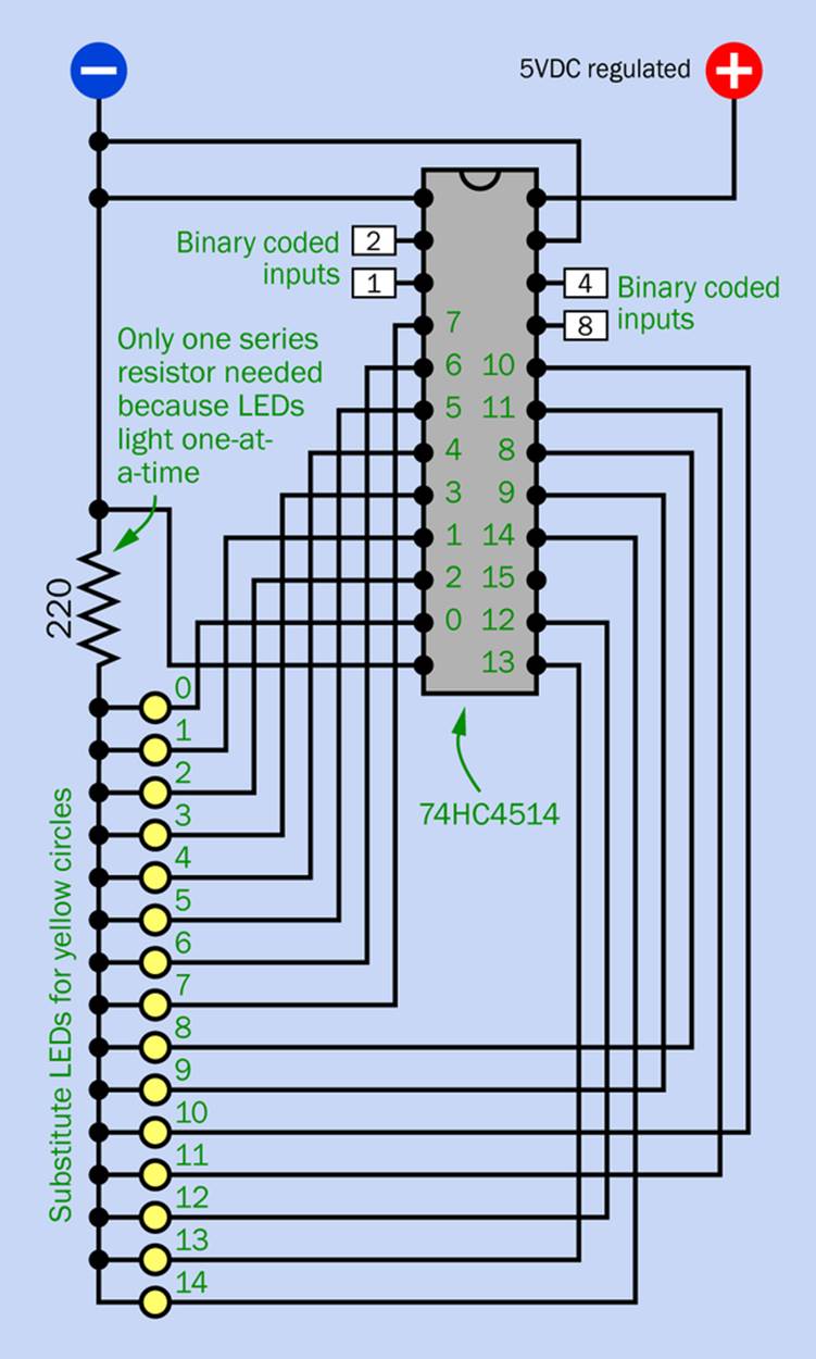
Figure 25-1. Binary-coded outputs from the adder in Experiment 24 become inputs to the 74HC4514 decoder chip. Each of its decoded outputs, from 0 through 14, is connected to an LED. Because only one output is ever in a high state, all the LEDs can share one series resistor.
The easiest way to deal with this is to mount the LEDs farther down the breadboard, as suggested in the figure, where yellow circles represent the LEDs. If your LEDs do not contain series resistors, you only need one resistor to serve all of them, because only one LED lights at a time. Assuming the bus on your breadboard is divided into sections, all the LEDs can share the center section, which would be linked to the upper section of the bus by the series resistor.
So much for that! Now for the harder part.
DIPping In
For decimal data entry, you can use simple SPST on-off switches. There can be two rows of eight switches, with values 0 through 7. You’ll turn one switch in the first row and one switch in the second row to enter the two values that are to be added.
DIP switches are the simplest, cheapest, smallest option for this purpose. Normally, in a set of eight DIP switches, they will be numbered 1 through 8. You will have to renumber them from 0 through 7.
The eight wires from each bank of switches will go to the eight inputs of an 8-to-3 encoder chip. As you might imagine, this is opposite in function to a decoder chip. It takes an input on one of its eight input pins (with values 0 through 7) and converts it into a binary value on its output pins (with place values 1, 2, and 4). The outputs from one encoder can feed straight in to the adder circuit data lines labelled A1, A2, and A4, while the outputs from the other encoder will supply B1, B2, and B4. (See Figure 24-11.)
Figure 25-2 shows a schematic for wiring the two encoders. If you follow it carefully, it should work. But precisely why it works requires some explanation—especially if you notice that the switches are attached to negative ground instead of the positive side of the power supply. Why is this?
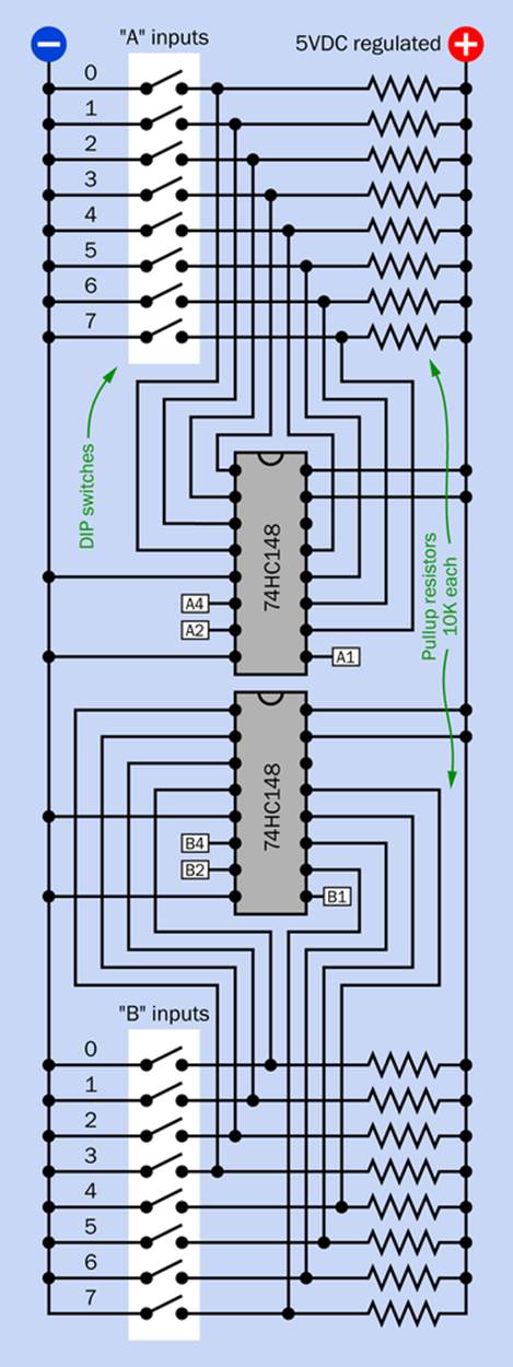
Figure 25-2. Outputs from two sets of DIP switches are connected with inputs of 74HC148 encoder chips. Note that inputs are logic low and resistors are for pullup, not pulldown. This is opposite to most logic chips.
Introducing an Encoder
Encoders have become relatively rare, and the ones still listed by suppliers use active-low logic. In other words, a low input or output represents a 1, and a high input or output represents a 0. This is irritating, because the chip has to work with the adder circuit, which uses conventional active-high logic. Without going into the historical reasons why encoders are made this way, I can still use the most common chip, the 74HC148, so long as I work around its quirks. Its pinouts are shown in Figure 25-3.
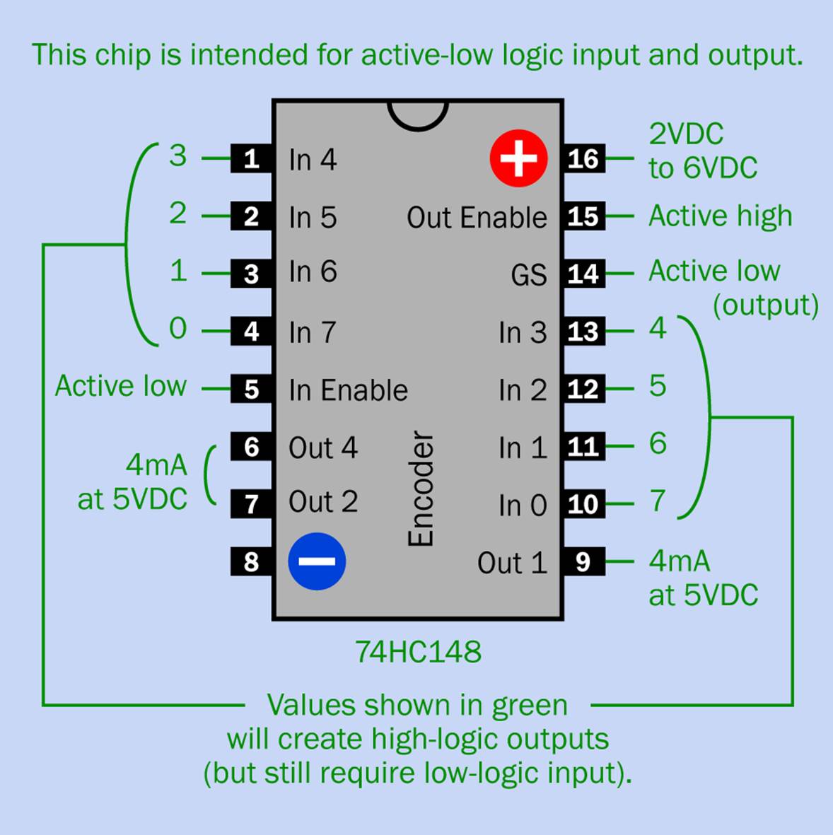
Figure 25-3. Pinouts for the 74HC148 encoder chip. See text for details about input and output.
There is a trick to get active-high outputs from the encoder. You reverse the sequence of the inputs. This is shown by the green numbers in the pinout diagram.
Are you confused, yet? Let me summarize. To get our usual, preferred, active-high logic output from the 74HC148:
§ Assign value 0 to input pin that has value 7.
§ Assign value 1 to input pin that has value 6.
(And so on, for intermediate values.)
§ Assign value 7 to input pin that has value 0.
Each input will still be active low. There’s no way around this. The reverse-numbering trick only fixes the outputs so that they are active high (which is what the rest of our circuit will understand). Therefore, as shown in Figure 25-2, pullup (not pulldown) resistors are applied to all the input pins, to keep them normally high (representing 0 values). The DIP switches are connected with negative ground so that when you turn a switch “on,” it provides the necessary active-low signal to the chip (representing a 1 value).
Other Encoder Features
Just to make things more interesting, the 74HC148 has some additional confusing features. There is a “Group Select” pin, identified as “GS” on most datasheets. It is an output pin that goes active low when the chip is processing an input. Because it is an output pin, you don’t have to worry about it, and you can leave it unconnected.
As for the two Enable pins, the input enable (often referred to as EI on datasheets) is active low, so I have tied it to negative ground. The output enable is active high (why, I don’t know), so I have tied it to the positive side of the power supply.
At this point you may be wondering if there are still some practical applications for encoder chips. Indeed, they have a possible use in industrial control processes where, for example, an item is moving past a series of sensors that are either “on” or “off.” If you are using a microcontroller that has a limited number of inputs, you could connect the sensing devices through an 8-to-3 encoder chip, and reduce the inputs to three. The power of this technique increases radically if you have more inputs, because you can chain encoder chips together, and if you double the number of inputs, the number of binary output lines only increases by one. This is because the place value of each digit in a binary number is double the place value of the digit that precedes it. Because the power of place values isn’t readily appreciated, I’m going to go into that for a moment.
Background: The Power of Binary
So far in this book we have only dealt with binary inputs and outputs that have place values of 1, 2, 4, and 8. The doubling of place value from each digit to the next may not seem particularly significant, because our 10-based human counting system is so much more powerful, with place values in multiples of 10. Still, the process of doubling can have unexpected consequences.
In an 8-bit binary number, the leftmost digit has a place value of 128, and the whole set of digits can represent any value from 0 through 255. These values are very common in computing. A byte of computer memory usually consists of eight bits. A typical JPEG consists of three colors (red, green, and blue), each of which is represented with a value ranging from 0, meaning “completely dark,” to 255, meaning “maximum brightness.” Maybe 256 color shades don’t sound like a lot, but because the three colors can vary independently, the total number of combinations is:
256 * 256 * 256 = 16,777,216
If you have ever heard that a computer video card can create “16 million colors,” now you know why.
If we increase the number of binary digits, the situation becomes more interesting.
A 16-bit binary number can represent any value from 0 through 65,535.
A 32-bit binary number can have a value slightly above 4 billion—which is why a computer with a 32-bit operating system is usually unable to address more than 4 gigabytes of RAM.
Regarding the term “gigabyte”: the international definition of “giga” is 1 billion, but in computer memory, “giga” means a binary number consisting of 1 followed by thirty zeroes. This translates into 1,073,741,824 in decimal notation. The situation originated when a kilobyte was defined as 10000000000 binary, which is 1,024 decimal. A megabyte became 1,024 kilobytes, and a gigabyte became 1,024 megabytes. But in hard drives, a gigabyte is simply 1 billion decimal. Just in case you were wondering.
But getting back to the power of binary numbers—
I own a little $10 calculator that can represent decimal numbers as high as 999,999,999,999, or almost 1 trillion. How many binary digits must the calculator use internally to deal with this? I think just 41 bits are sufficient, assuming that one of those bits is allocated to show whether a number is positive or negative.
Even though binary code is restricted to 1s and 0s, it is capable of handling very large numbers.
Background: Encode Your Own
If you prefer not to use the 74HC4514 chip, you can create your own encoder, because the logic is very simple. It is shown in Figure 25-4. Follow the connections and you’ll see that pressing (for example) the switch with value 6 will activate binary outputs with values 4 and 2. Note that if you actually create this circuit, you will need to add a pulldown resistor on the output from each switch.
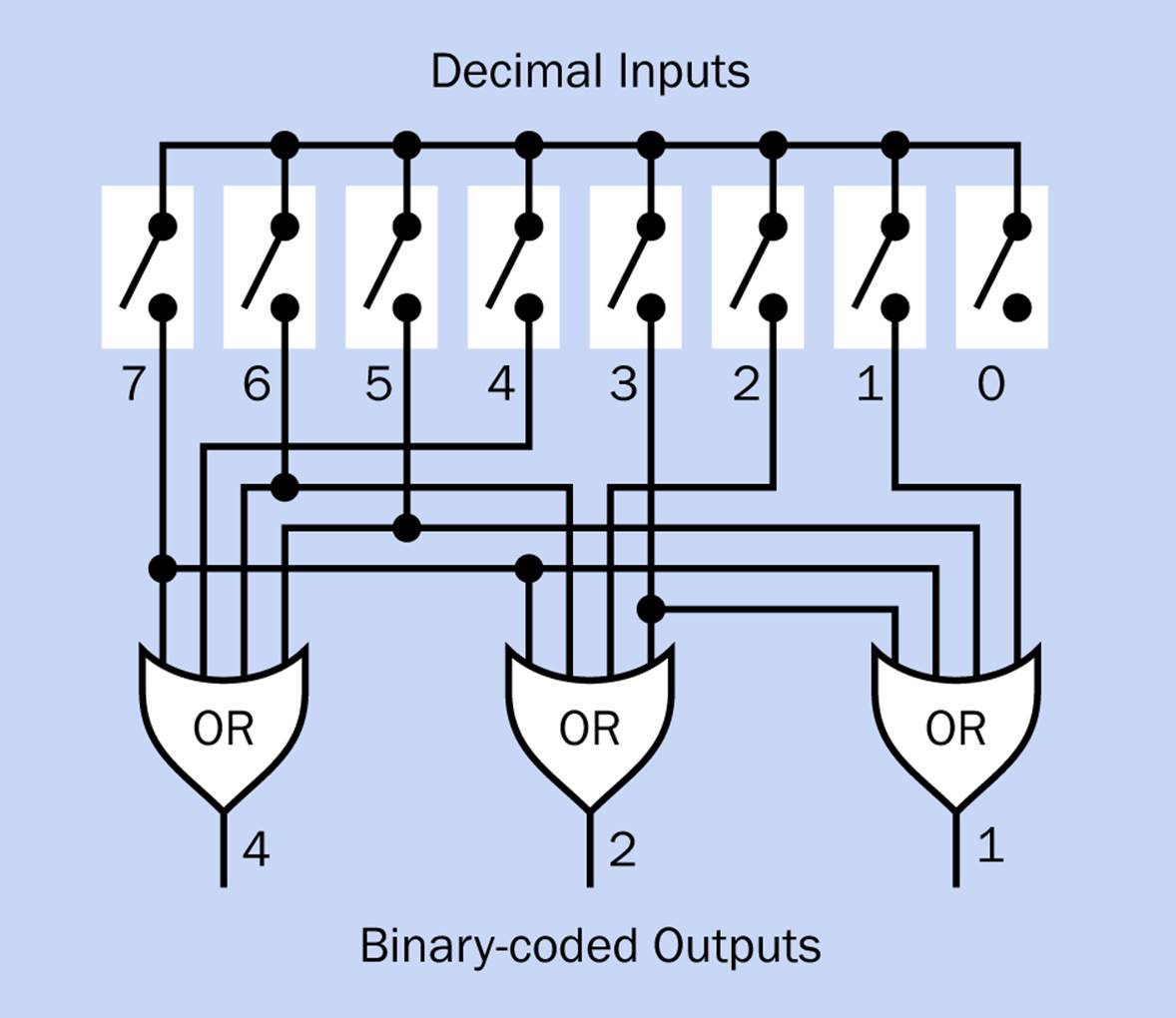
Figure 25-4. Three four-input OR gates are all you need to emulate the behavior of an 8-to-3 bit encoder chip. Pulldown resistors (not shown here) would be added to the output of each switch.
Maybe you remember when I wanted to use a four-input OR gate, but it didn’t exist in the HC family. (See Chapter 20.) Would that be a problem here? No, because in this application, the OR outputs are not driving LEDs. They will be connected with the inputs of other chips in the adder circuit in Figure 24-11. Therefore, you can use chips from the old CMOS 4000B series. Two 4072B dual-four-input OR chips will do the job.
I like to minimize the chip count, so I specified the 74HC148 encoder instead of using two chips containing OR gates.
Make Even More: Other Input Options
For data entry, instead of using DIP switches, you could substitute eight-position rotary switches. They would prevent the selection of more than one number at a time—but they wouldn’t fit on your breadboard and would be more expensive.
You could also consider keypads, especially if you can find a couple that are not matrix encoded. A matrix-encoded keypad is designed to be scanned by a microcontroller. An unencoded keypad gives you a separate output line for each digit that you enter, but this type of keypad is less common. (I used one for an experiment in Make: Electronics).
Lastly, you could use the type of input device that provides a thumbwheel to select a number, typically 0 through 9 but sometimes 0 through 15. Confusingly, these are often referred to as “encoders.”
Can We Switch It?
Now that I’ve decimalized the inputs and outputs of the binary adder, you might think that this project has gone as far as it can go—but in fact I have one more suggestion. No doubt you will remember that I described versions of the Telepathy Tester, the Rock, Paper, Scissors game, and Ovid’s Game that used switches instead of logic chips. Surely, I’m not thinking of using primitive electromechanical switches to build a binary calculator?
Actually, I can’t resist the idea. I won’t include this as a separate experiment, because it’s really a Make-Even-More digression that I am including just for fun—at least, my idea of fun. I like the idea of a binary adder that contains no electronics whatsoever (unless you count the LEDs).
Also, while this kind of thing has no practical application, it helps you to think as a computer thinks, which is a prerequisite for designing good logic circuits (or good software). Therefore, I think it has some value.
Make Even More: Switched Binary Adder
I showed you the switch equivalents of logic gates in Figure 18-1. Since a half adder can be built from an XOR gate and an AND gate, you can represent it with only two switches, as shown in Figure 25-5.
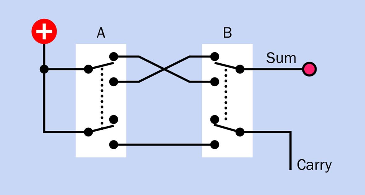
Figure 25-5. The function of a half adder can be emulated with a pair of DPDT switches. A grounded LED, with series resistor as required, should be substituted for the “Sum” indicator.
When switches are used as a substitute for logic gates, an input consists of pressing a switch. So, to enter the binary addition sum 1 + 0, you would close the lefthand switch while leaving the righthand switch open. This correctly gives an answer of 1 by illuminating the LED, with no carry output. And if you entered 1 + 1 by pressing both switches, you’d get the correct answer 10, represented by a carry output while the LED stays dark.
This seems easy enough, but a full adder is more problematic. Refresh your memory of the logic diagram for a full adder by taking a look at Figure 24-5. The top part is exactly the same as the half adder, which I just dealt with. No problem there. But the output from the first XOR gate goes to another XOR, where it is compared with the carry from the previous place.
The problem is, we are now using fingers pressing switches as inputs. But the second XOR only has electrical inputs—nothing that can be pressed by a finger.
Here’s another problem. A low output can be interpreted by a logic gate just as easily as if it were a high output. But when switches are used, a low output becomes an open switch, which cannot be interpreted, because its state is indeterminate.
My answer to both these problems is to have an active “no carry” output from the half adder, as well as a “carry” output. This will provide voltage that each new stage of the adder can either block or pass along.
A revised half-adder schematic is shown in Figure 25-6. The “no carry” output is active if neither switch is pressed, or if either switch is pressed, but not both. The “carry” output is only active if both switches are pressed, so the “carry” and “no carry” outputs are always the inverse of each other.
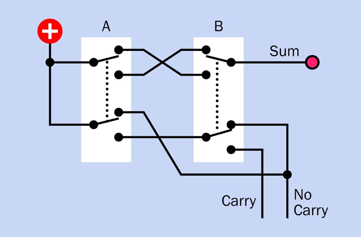
Figure 25-6. The previous schematic for a switched half adder has been revised to include a “No Carry” output to provide voltage for the next stage.
Making a Table
The next step is to nail down exactly what we want from a full adder. To do that, I made a little table, shown in Figure 25-7. This shows the three possible outputs that the adder can create and all the input combinations that can create each output.
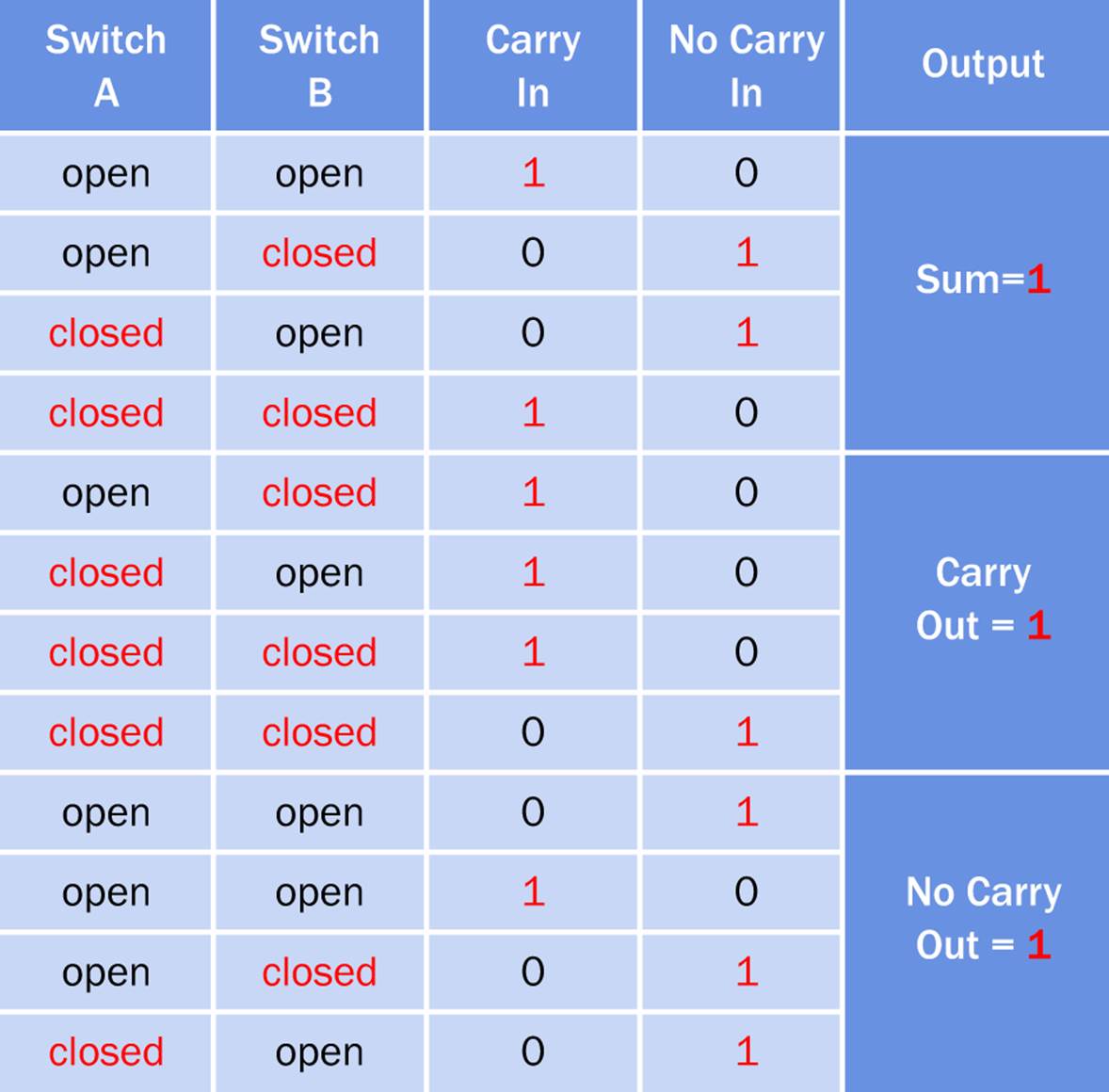
Figure 25-7. The outcomes from a full adder, for all possible input combinations.
For instance, the second line of the table shows that when Switch A is open (representing a 0 input), and Switch B is closed (representing a 1 input), and there is no carry coming in from the previous place, then Sum = 1. The eleventh line of the table shows that the same combination of inputs results in a “No Carry” voltage going out. This makes sense because if you have one switch being pressed, and no carry coming in, there should be no carry going out.
Switch Specification
I was able to figure out (with some difficulty) a pattern of switches that would match the requirements shown in the table. The schematic is shown in Figure 25-8.
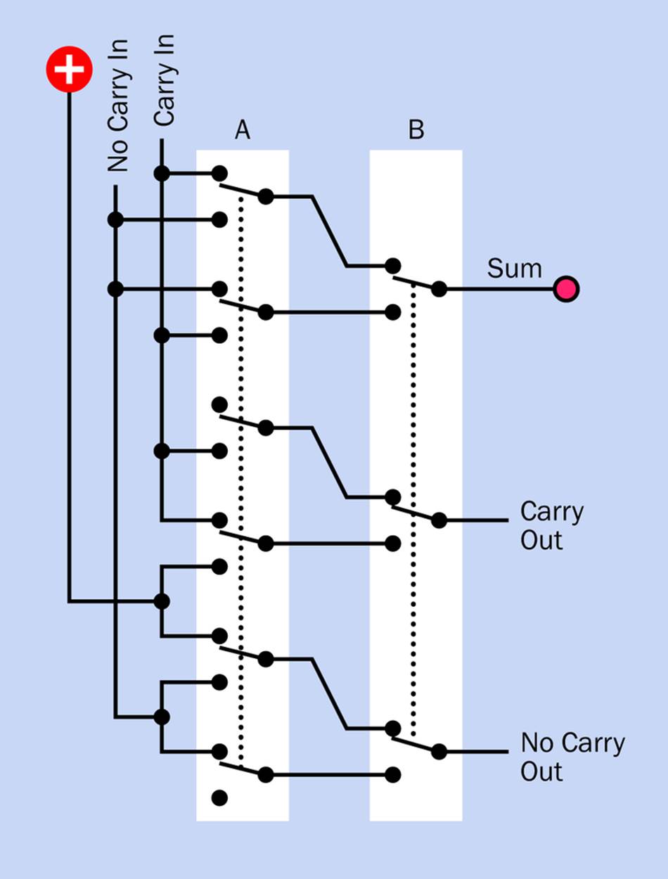
Figure 25-8. A full adder built from a six-pole switch and a three-pole switch, creating the outputs specified in the preceding table.
As you’ll see, this requires a six-pole switch and a three-pole switch. Such switches are readily available in the latching pushbutton format, but I haven’t finished, yet. I want to add an LED to each switch, to show when it is pressed.
This is easy enough in Switch B, because right now it only has three sets of contacts, allowing me to add another set to activate the LED. But adding extra contacts to Switch A would be more problematic, as it already has six poles. Some eight-pole switches do exist, but they tend to be expensive unless you can dig some up from a Chinese source on eBay.
After pondering this problem for a while, I recalled that a computer programmer named Graham Rogers, in England, has always shared my interest in puzzles—and because Graham is almost as obsessive as I am, he created his own switched version of a binary adder a few years ago. I couldn’t find a schematic of it, so I checked with him and found that he and I had come up with the same basic circuit independently. However, he swapped the switch functions that create the sum, which freed up a pole on the lefthand switch to drive an LED.
This revised circuit is in Figure 25-9. It’s not quite as simple as the previous version, but it only requires six-pole switches.
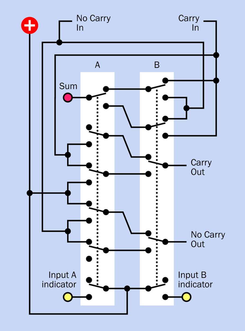
Figure 25-9. Revised schematic for a switched full adder, allowing allocation of an extra pole in each switch for an LED indicator.
You can string together as many of these switched adders as you like, to handle binary numbers of any size. The version that Graham built is capable of adding two eight-bit numbers (two bytes) and can also do subtraction. I can’t remember the rules for subtraction in binary code, so I’ll leave that problem to you.
Make Even More: Other Possibilities
Can the wiring for a switched binary adder be simplified any further? Can the number of switch contacts be reduced? I don’t think so, but I’d like to be proved wrong. If you come up with a plan, let me know.
Now, I can’t resist asking—could we get rid of the OR gates in Figure 25-4 and build an encoder just from switches, to process decimal input and turn it into binary? It should be possible. Any time you see a simple set of gates like those in Figure 25-4, you can feel fairly sure that they can be emulated with switches.
Indeed, this is quite easy. The circuit is shown in Figure 25-10.
The output from this circuit could be used for input to the electronic version of the adder in Figure 24-11, if you don’t mind getting rid of the DIP switches and substituting an assortment of SPST, DPDT, and 3PDT switches.
However, I see no way to interface it with the switched adder. The problem is that in a switched adder, the input switches aren’t just providing input—they’re doing dual duty, performing the arithmetical operations. I’d be very surprised if a decimal-input switched adder were possible, using switches with a reasonable number of poles. On the other hand, I cannot prove that it’s impossible, and human ingenuity sometimes produces amazing results.
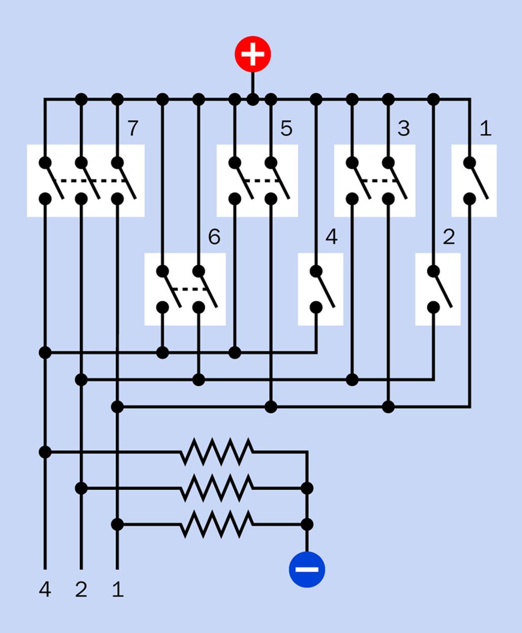
Figure 25-10. The switched circuit shown here would emulate the function of an 8-to-3 encoder chip.
Remember that before the modern era of electronic calculators, adding machines (which could also do multiplication sums) were entirely mechanical. When you looked inside, you found an insanely complicated assembly of gears and levers, and of course the designs were all done with pencil and paper, long before the era of computer-aided design.
Going further back, Charles Babbage’s “Difference Engine” (the first part of which was built in 1832) was a calculating machine, leading Babbage to plan his “Analytical Engine,” a general-purpose, programmable mechanical calculating machine. Vision combined with persistence can achieve remarkable results, if someone has enough time and money to work on a problem.
But I’m going to move on, now, to ring counters and shift registers. These will lead to an in-depth exploration of randomicity, ultimately involving various types of sensors, which will be the closing topic of the book.
All materials on the site are licensed Creative Commons Attribution-Sharealike 3.0 Unported CC BY-SA 3.0 & GNU Free Documentation License (GFDL)
If you are the copyright holder of any material contained on our site and intend to remove it, please contact our site administrator for approval.
© 2016-2026 All site design rights belong to S.Y.A.