Make: More Electronics (2014)
Chapter 24. Experiment 24: Adding It Up
Before I move on from logic gates to other topics, I wouldn’t be doing a thorough job if I didn’t show you the most fundamental logic application: adding numbers. You already have a calculator, which is far more powerful than anything you are likely to build yourself; but in my experience, there is something slightly magical about putting together your own little circuit that can perform basic arithmetic.
The Five Rules of Binary
Because logic chips only have two states—low and high—they are ideal for representing the 0s and 1s of binary code. Therefore, to make a circuit that adds numbers, you have to use binary addition. The good news is that there are only five rules for adding binary numbers, three of which are obvious. I’ll deal with those first:
§ Rule one: 0 + 0 = 0
§ Rule two: 0 + 1 = 1
§ Rule three: 1 + 0 = 1
I think you’ll have no problem agreeing with these. Now for the fourth, which looks a bit odd:
§ Rule four: 1 + 1 = 10 binary
If you’re reading this as “one plus one equals ten,” this is not correct. You have to let go of your ten-based thinking! The word “binary” in rule four tells you that 10 has nothing to do with “ten,” because 10 is a binary number.
We all know that 1 + 1 = 2, so why don’t we just write 2? Because in binary code, we only have 1s and 0s. So, we apply the fifth rule:
§ Rule five: when you have an output that would be decimal 2, write 0 as the sum, and carry 1 over to the next place on the left, where it has a place value of two.
You’ve run into the concept of place value previously in this book, when I talked about binary inputs to chips, such as a decoder. In binary counting, a numeral 1 has a place value of 1 in the rightmost place, 2 decimal in the next place to the left, 4 decimal in the next place, 8 in the next place—and so on.
So, 1 + 1 = 10 really means that the answer has no units in the rightmost place, and a value of 2 in the next place to the left.
The four possible combinations, when adding two binary digits, are shown in Figure 24-1.
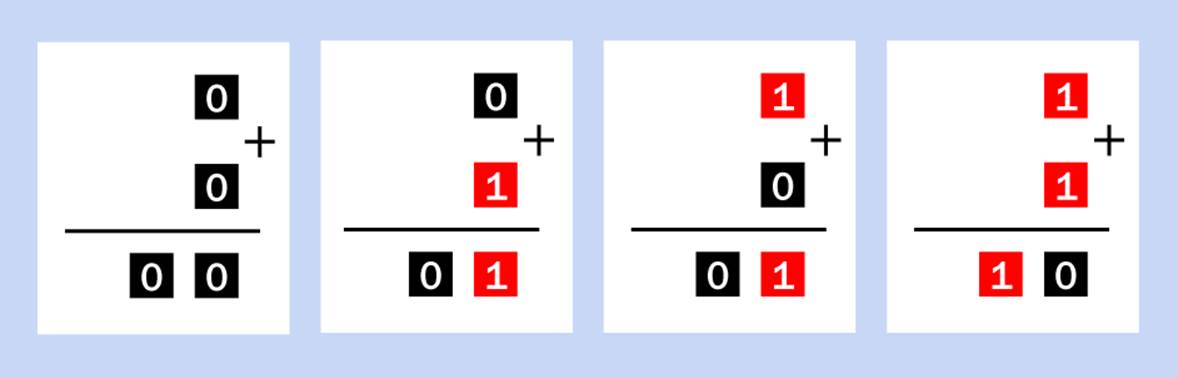
Figure 24-1. The basic rules of binary addition, using 1-bit binary numbers.
Now take a look at Figure 24-2 and you’ll see that even when we have to handle binary numbers consisting of two digits each, the same rules still apply. This diagram shows every possible combination of two two-bit numbers.
There’s only one issue that may seem unclear. What exactly is going on when we add 11 + 11 in binary?
As always, we start in the rightmost place. We add 1 + 1 and write a zero, and carry 1 to the left. But in that place, there is already another 1 + 1 waiting to be added. So now we have to deal with 1 + 1 + 1.
Well, we know that 1 + 1 is 10 binary. So when we add another 1 to that, we get 11 binary. You can see this in the very last example in Figure 24-2.
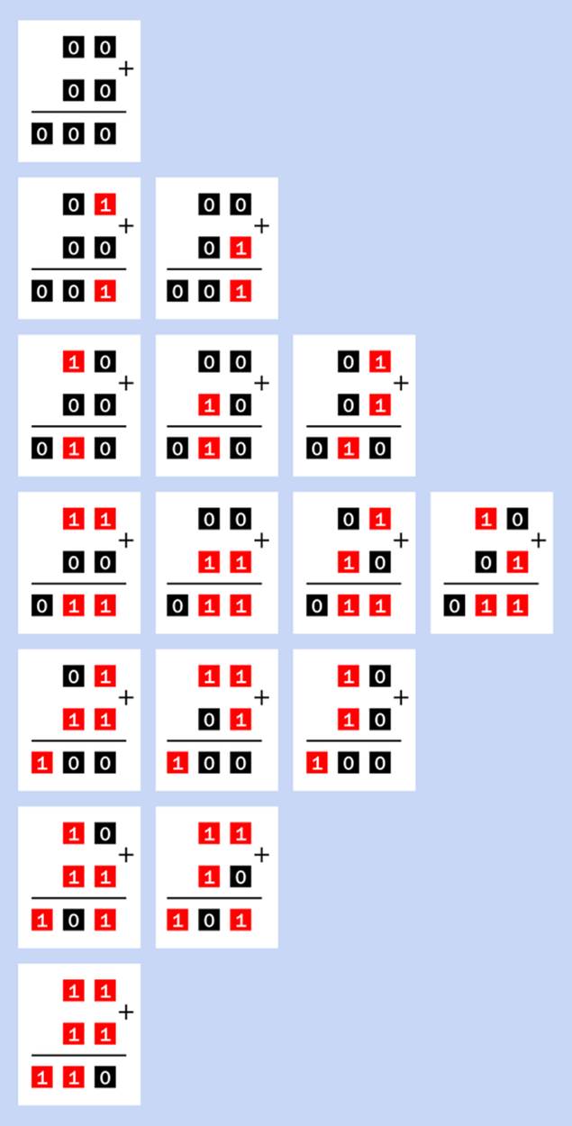
Figure 24-2. The basic rules of binary addition, using two-bit binary numbers.
From Bits to States
So much for the rules of binary arithmetic. You now have all you need to know to build a binary adder (and if binary numbers don’t seem very user friendly, I’ll show you how to convert to and from decimal numbers in the next experiment).
Let’s consider how we can use logic chips to emulate the binary rules, using the high state of a logic gate to represent a 1, and the low state to represent a 0. I can rewrite the first four rules of binary addition using words instead of numbers, like this:
§ Low input + low input = low output
§ Low input + high input = high output
§ High input + low input = high output
§ High input + high input = low output (and carry high to the next place)
What does this remind you of? Well, by George, if we forget about the “carry” operation for a moment, this is a precise description of the inputs and outputs of an XOR logic gate! Just apply the two numbers to be added as low and high states to the XOR inputs, and the XOR output will be correct. We can represent it with an LED that indicates 0 when it is off and 1 when it is on.
Now, what about carrying 1 to the next place on the left? I could say:
§ High input + high input = high carry
§ All other input combinations = low carry
What does this remind you of? An AND gate, of course! If this is tied in to the two inputs, its output can be a second LED.
Figure 24-3 shows how the gates are combined to add any two single binary digits, which I have represented with the imaginative names “A” and “B.” Figure 24-4 shows the four possible combinations of inputs, and the resulting outputs, with red indicating a 1 and black indicating a 0.
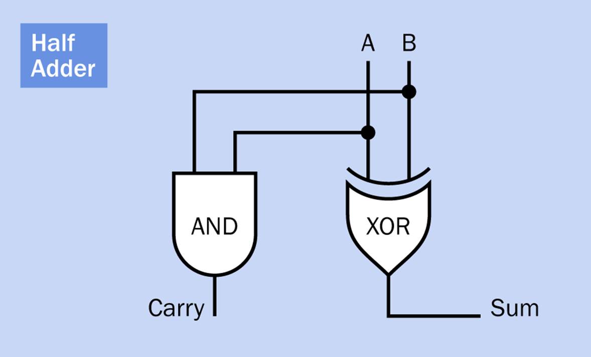
Figure 24-3. Probably the simplest way for logic gates to add two binary digits, and generate a “carry 1” if necessary, is with an XOR gate and an AND gate.
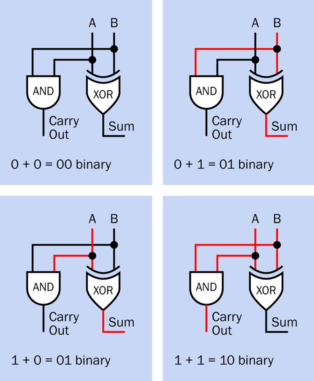
Figure 24-4. The four possible input combinations to a half adder, and the resulting outputs. Red is interpreted to mean 1, while black means 0.
This very, very simple circuit is known as a “half adder.” It can only be used in the rightmost place of a binary addition sum, because it cannot process a carried number coming in from a place farther right.
But what if there is a place farther right, which may generate a carry-1 output? How do we process that?
We need a “full adder.”
This is a bit more tricky. We can only compare two inputs at a time using an XOR logic gate, but we have three numbers to deal with: two binary digits as inputs, plus a carry digit (which may be 0 or 1) from the previous place in the calculation. We might find ourselves trying to deal with 1 + 1 + 0 or 0 + 1 + 1 or any other combination up to 1 + 1 + 1.
The way to do this is by breaking the process into two steps. Figure 24-5 shows how. You’ll notice that it is really two half adders, each consisting of an AND gate and an XOR gate, plus an OR gate that says we’ll carry 1 out if either of the half adders requires it.
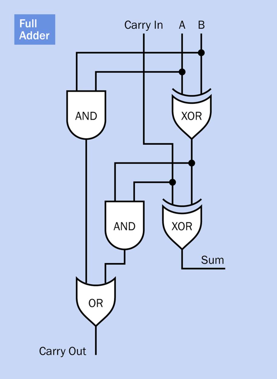
Figure 24-5. A full adder receives a carry digit from the previous stage and adds it to two new binary digits.
The first XOR adds two binary inputs, as before. Now we take the single-digit output from the XOR and add the incoming carry to it. This means placing another XOR gate under the first.
There will be two circumstances under which our full adder will have a new outgoing carry:
1. If we have 1 AND 1 as our binary inputs, we will carry 1 out using the first AND gate—as usual.
2. OR if the output from the first XOR is 1, AND we also have an incoming carry of 1, we will carry 1 out.
There are eight possible combinations of two inputs and an incoming carry. I have shown four of them as examples in Figure 24-6.
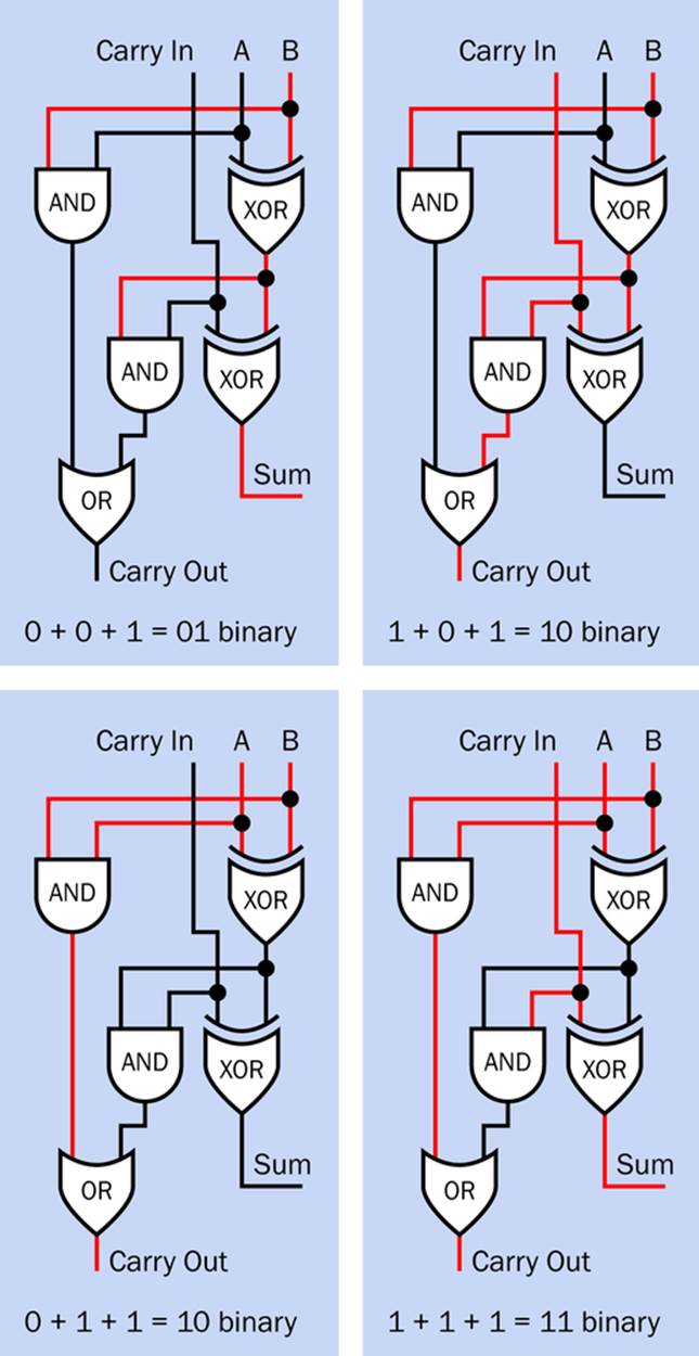
Figure 24-6. The three inputs to a full adder can have a total of eight different combinations. Here are four of them, illustrating how the adder operates.
You are now almost ready to build your own adder. But first, a small digression.
Background: The NAND Alternative
Because logic gates can emulate each other, depending on how they are wired together, the XOR/AND combination is not the only way to build a half adder. I used it because I think it’s the easiest to understand, but NAND gates are commonly used. This alternative requires more gates (five instead of two, to make a half adder, and nine instead of five, to make a full adder) but the great advantage is that NANDs can do the job all on their own, with no gates of any other types. An all-NAND computer is easier to construct in some ways, so NANDs are often thought of as the most fundamental gate in computing. They were assigned part number 7400 in the long series of 74xx logic chips.
Figure 24-7 shows how five NANDs can form a half adder, while Figure 24-8 shows how nine can make a full adder. Once again, the full adder is composed of two half adders stacked up.
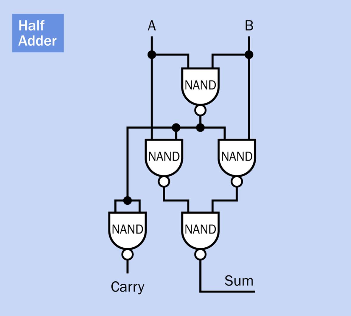
Figure 24-7. A half adder can be constructed entirely from NAND gates.
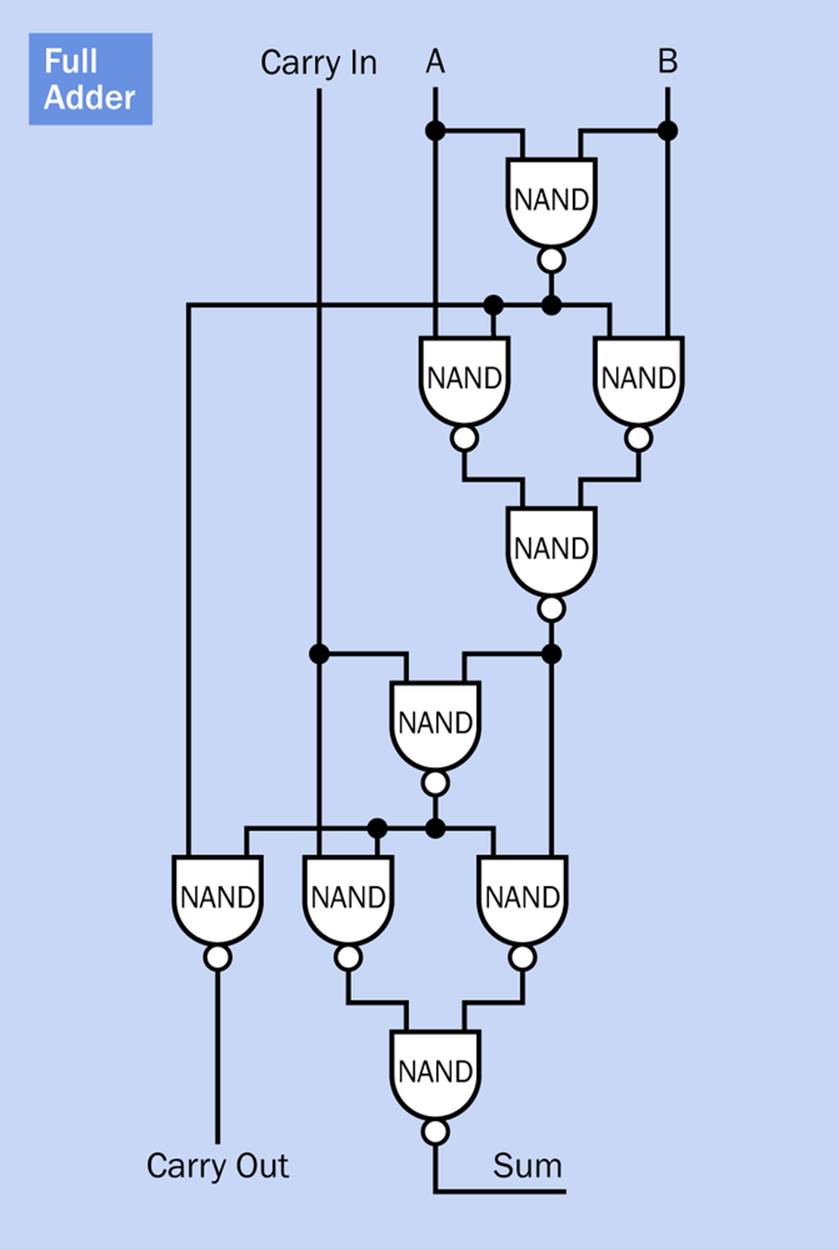
Figure 24-8. A full adder can also be constructed entirely from NAND gates.
If you are methodical and patient, you can print several copies of these diagrams and use red ink to trace logic paths through them to verify that the output is correct for each of the eight possible combinations of inputs. Personally, I’m not going to do this. I’m going to stay with the XOR/AND combination, because NANDs give me a headache.
Your Own Little Adder
So where’s the hands-on activity, here? Normally I suggest putting components together first, and then figuring out why they do what they do. That’s the basis of what I like to call “Learning by Discovery.”
In this case, I felt that if I didn’t explain the theory first, nothing would make any sense. But you can go right ahead now and build a calculator that will add two three-digit binary numbers and deliver a four-digit output.
This will use one half adder and two full adders. They will require a total of five XOR gates, five AND gates, and two OR gates. There are four two-input gates on a quad two-input chip, so we’ll be leaving quite a few gates unused. In fact, we will have enough gates on the chips to create a calculator capable of adding four-digit binary numbers and delivering a five-digit output. But I don’t want to do that, because an output of five binary digits will be too big for the next little adventure that I have in mind. Maybe you remember what I promised to show you in the next experiment—and it will be much easier if we only have four binary digits to be processed.
Breadboard Addition
In Figure 24-9 I have assembled a half adder and two full adders to make a complete logic diagram for a three-bit adder with a four-bit output.
The two binary numbers to be added are entered by pressing switches at the top of the diagram. I have used darker blue areas to identify the switches that enter the first three-digit number, and switches that enter the second three-digit number. The place value of each digit is shown in green.
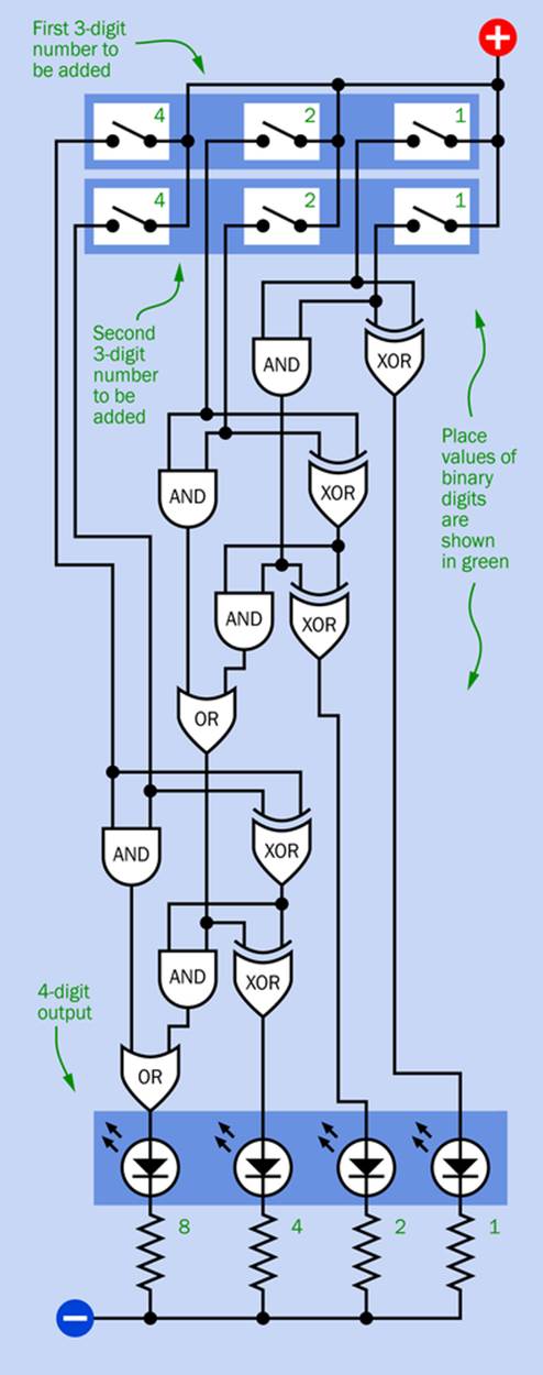
Figure 24-9. Logic diagram showing gates that can sum two three-bit binary numbers, with a four-bit binary output.
Logic gates have been shifted around just a little, compared with the previous diagram showing a full adder. But the connections are still the same.
To take a random example, if your little arithmetical operation is 5 + 7 decimal, you would close switches 4 and 1 in the upper row (to make 5), and switches 4, 2, and 1 in the lower row (to make 7). Assuming that the adder works properly, you should immediately see LEDs 8 and 4 lighting up to give you the answer of 12 decimal, while LEDs 2 and 1 would remain dark.
Figure 24-10 shows the pulldown resistors that you will have to include when you build this circuit so that none of the inputs to logic gates will float when switches are open.
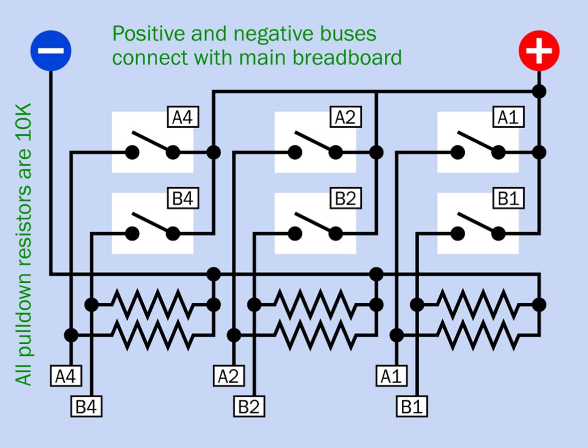
Figure 24-10. The input switches for the three-bit adder, with pulldown resistors.
The switches and their outputs are labelled to match the inputs to the main part of the circuit, which is shown in Figure 24-11. Little yellow circles have been used as a space-saving alternative to the usual LED symbols. Remember to add series resistors between your LEDs and negative ground, if you are not using LEDs that contain their own resistors.
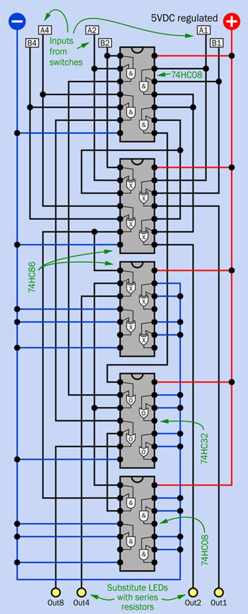
Figure 24-11. Breadboard schematic for components in the three-bit adder with a four-bit output. Labels at the top are for connection with input switches, shown separately. Numbers beside input letters indicate their binary place values.
Because there are a lot of parallel conductors in this schematic, I tried to reduce the confusion by using red and blue to identify the two sides of the power supply.
A photograph of the completed project is shown in Figure 24-12. Dual-inline switches (DIP switches) were used for inputs, because they take so little space on the board.
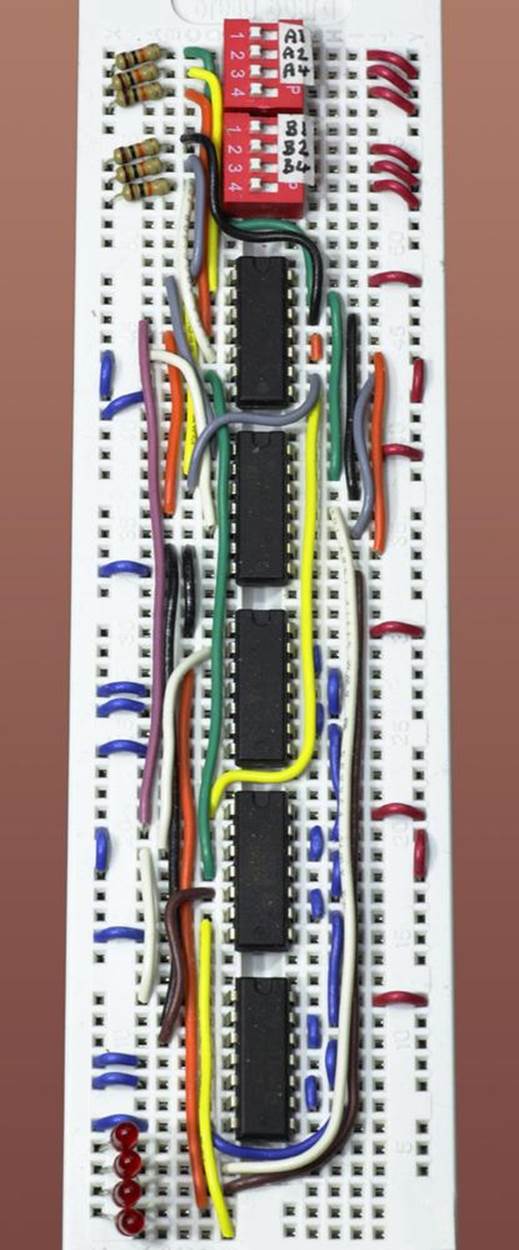
Figure 24-12. The completed breadboard layout of the 3-bit adder. The DIP switches have place values 1, 2, and 4 for each of the binary numbers (A and B) to be added. The LEDs at the bottom have place values 1, 2, 4, and 8, reading from top to bottom.
So, now you have a real-life, solid-state adding machine—something which would have seemed utterly magical as recently as the 1930s. The only problem is, quite apart from its limited capability, it’s not very easy to understand, because you have to convert decimal numbers into binary to use them as inputs, and then you have to convert the binary outputs back into decimal. Moreover, you don’t even have a numeric keypad, let alone a keyboard.
Actually, the world’s first personal computer (the Altair 8800, marketed in kit form in 1975) required you to enter all data by flipping switches. This was known as “toggling in” a program. The computer didn’t have a keyboard because that would have required more chips to interface it with the computer, and chips were expensive!
I realize that it’s not 1975 anymore, so maybe we can simplify the data entry ritual and enhance the display for your 3-bit adder. That’s the next experiment.
All materials on the site are licensed Creative Commons Attribution-Sharealike 3.0 Unported CC BY-SA 3.0 & GNU Free Documentation License (GFDL)
If you are the copyright holder of any material contained on our site and intend to remove it, please contact our site administrator for approval.
© 2016-2026 All site design rights belong to S.Y.A.