Practical Electronics: Components and Techniques (2015)
Appendix B. Schematics
Schematics are the lingua franca of electronics. Someone trained in electronics in China can look at a schematic created in Sweden and immediately understand what is being described by the symbols in the diagram. In its most basic form, a schematic shows the connections between the various components in an electrical or electronic device. More abstract forms can be used to describe functional relationships between components or subsystems or define an equivalent circuit.
The symbols used in electronic schematics have evolved over the years from early pictorial representations to the standardized symbols in use today. By the 1920s, most of the symbology used today was in regular use, with regional variations for some of the components. For example, even today, schematics created in places other than the US might use rectangles for resistors, along with other minor differences. The standard “IEC 60617 - Graphical Symbols for Diagrams” from the International Electrotechnical Commission (IEC) defines over 1,900 symbols, but obtaining a copy of the standard is rather pricey. This appendix describes a subset of the standard symbols in common use in the eletronics field.
An electronic schematic does not say anything about the physical arrangement of the components in a circuit. When you are reading a schematic and comparing it to an actual piece of hardware, it is not uncommon to find, say, R22 and R23 near each other on the schematic, but on opposite sides of the actual circuit board. A circuit’s physical arrangement is a function of packaging and circuit board design. How the circuit moves electrons around between the components is the domain of the schematic diagram.
Wires and Current Paths
Figure B-1 shows a variety of common wiring symbols used in schematics. A wire, or current path, is shown as a solid line. When two wires connect, the junction is indicated by a black dot. If there is no connection, the wire lines simply cross. Schematics created before about 1980 used ahump (or bump) to indicate that one wire crossed another without connecting. This is seldom seen today, probably due to the greater complexity of modern circuits with many wire paths in the diagram.
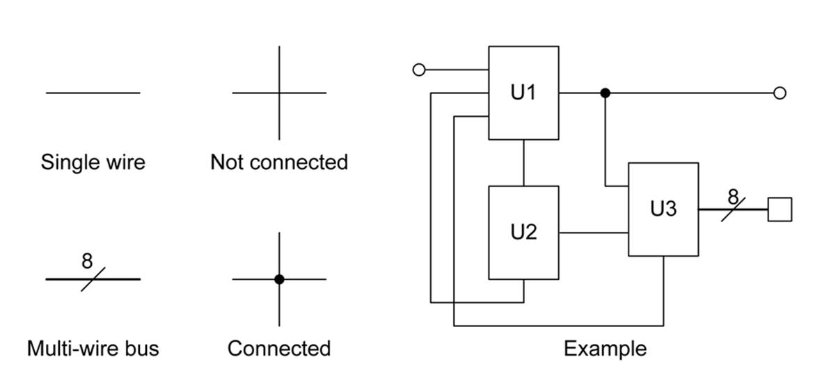
Figure B-1. Wiring symbology
To indicate a group of wires run in parallel (i.e., a bus), a heavy solid line is often used with a slash and a number. The number indicates the number of independent paths in the bus. This is commonly seen in digital circuits where 8, 16, or more paths might connect two or more digital components in parallel.
The wires that make up the connection paths in a circuit diagram are referred to as the net, or the netlist. Many schematic capture tools (some of which are discussed “Schematic Capture and EDA Tools”) can generate a netlist output for use as an input into other tools. When creating a schematic by hand or reading a schematic, you don’t usually need to worry about the netlist, but it can be important when you’re working with electronic design automation (EDA) tools.
Common Schematic Symbols
The symbols shown in this section are based on those found in various publications, such as the ARRL Handbook (published by the American Radio Relay League) and The Art of Electronics (Horowitz and Hill), and from many years of experience with creating and staring at schematics. They may, or may not, look like the symbols found in various schematic capture and EDA packages (see “Schematic Capture and EDA Tools”), but they are intentionally generic and should be close to what you will see in common usage.
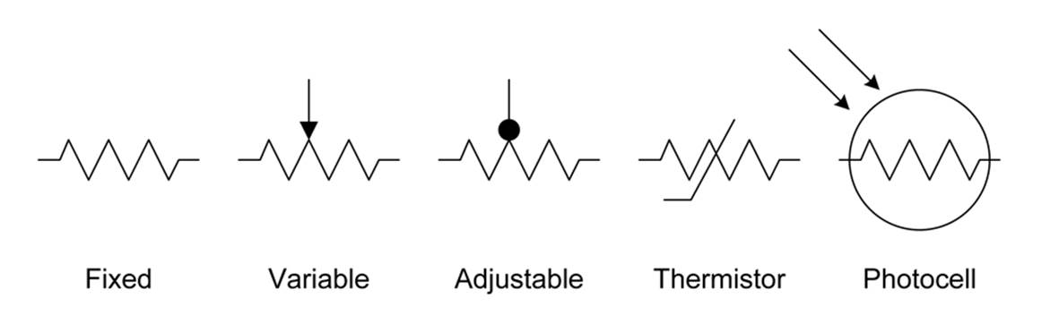
Figure B-2. Resistors
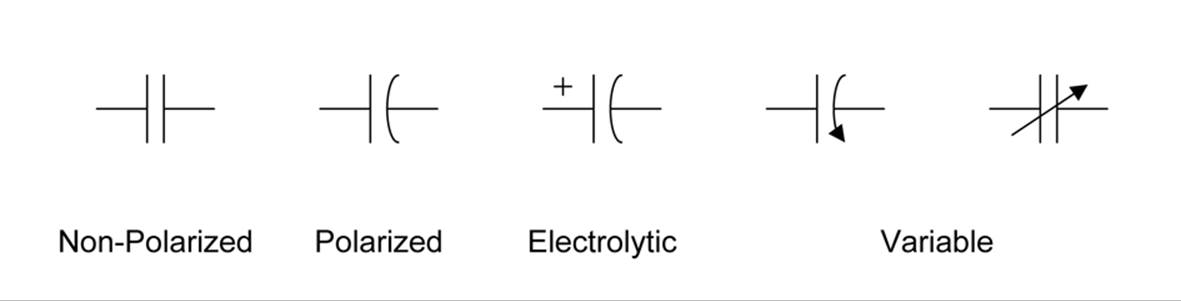
Figure B-3. Capacitors
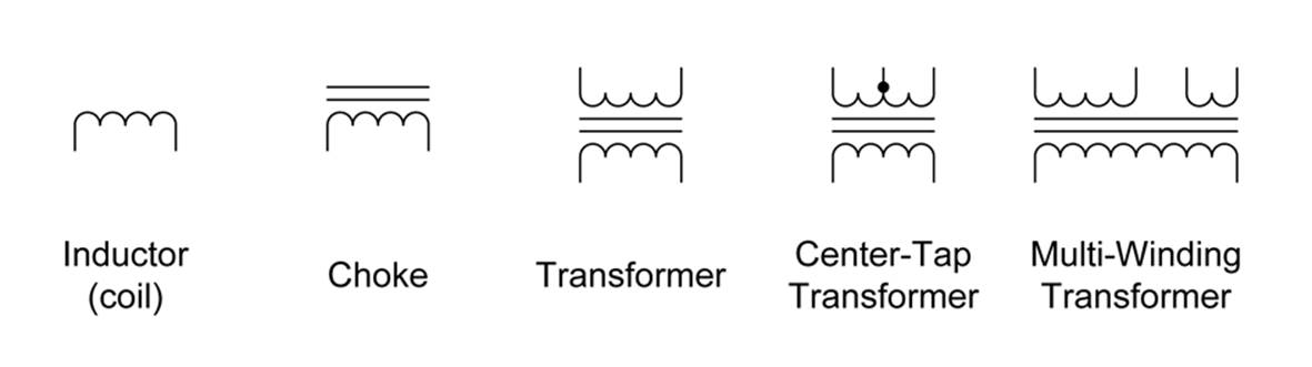
Figure B-4. Inductors
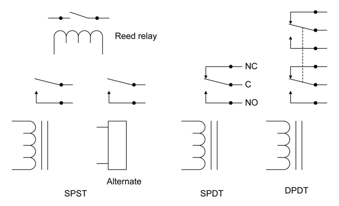
Figure B-5. Relays
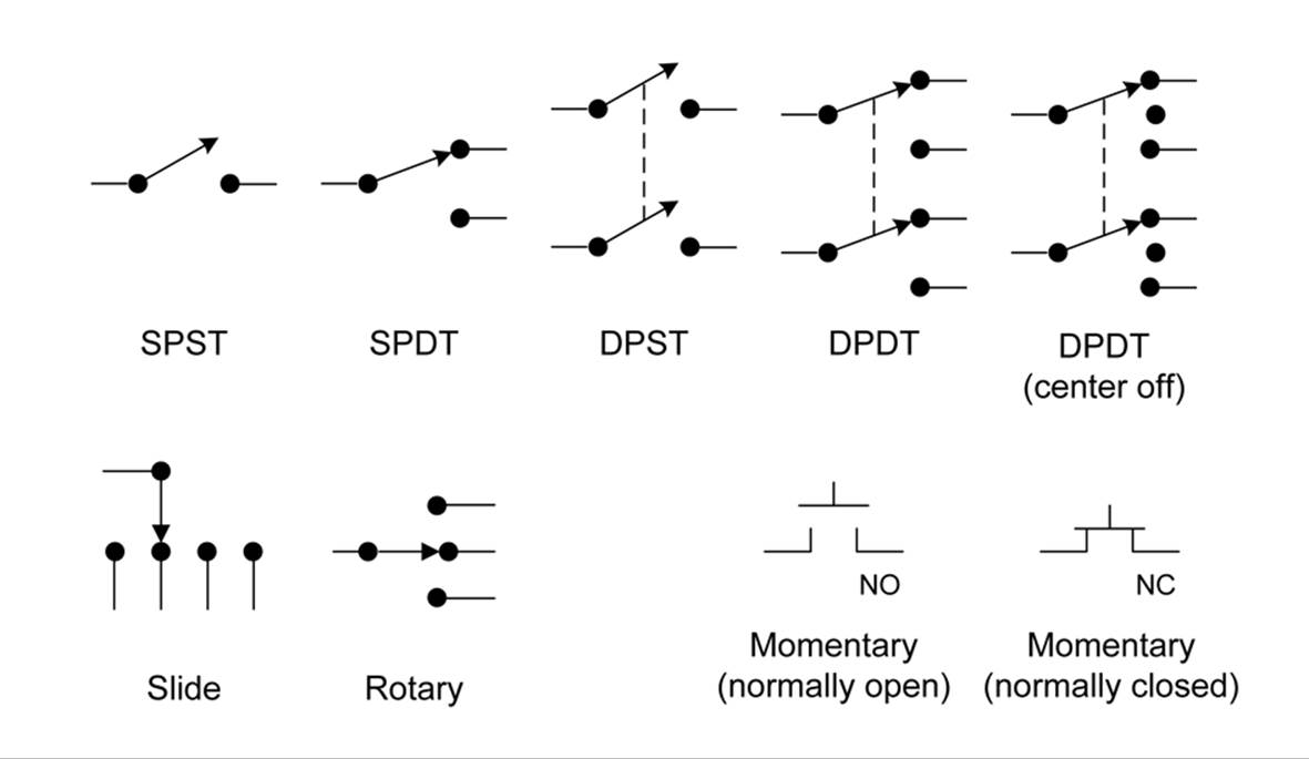
Figure B-6. Switches
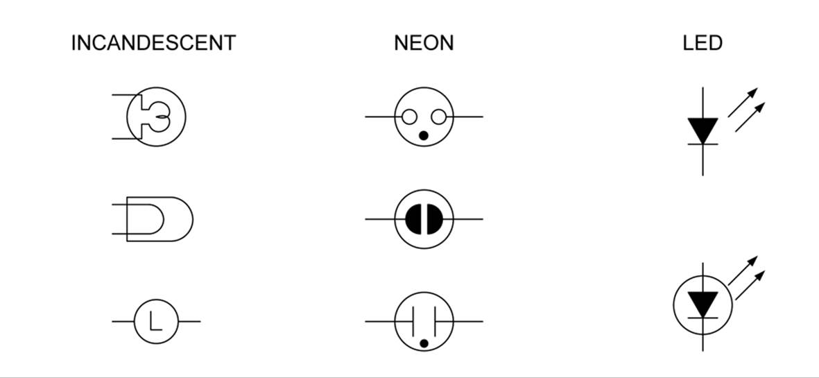
Figure B-7. Indictors and lamps
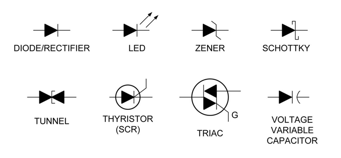
Figure B-8. Diodes and rectifiers
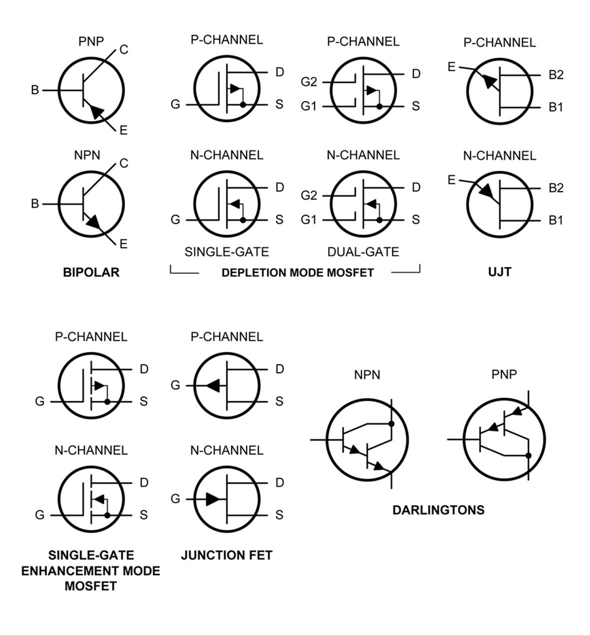
Figure B-9. Transistors
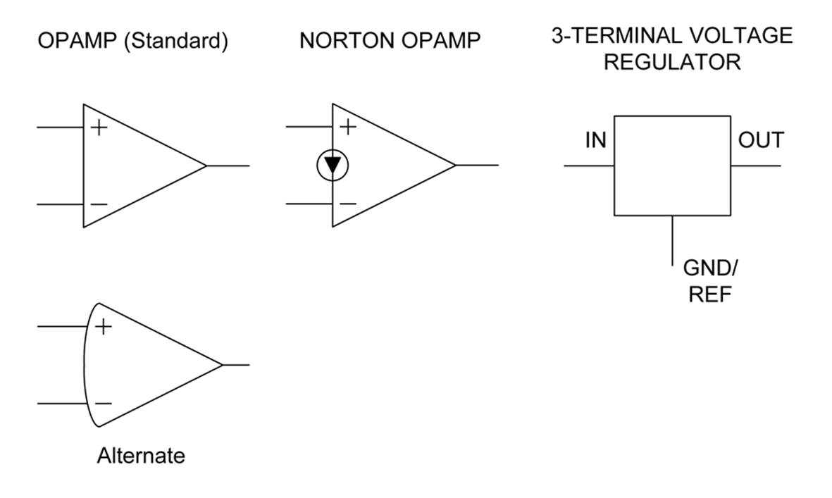
Figure B-10. Analog ICs
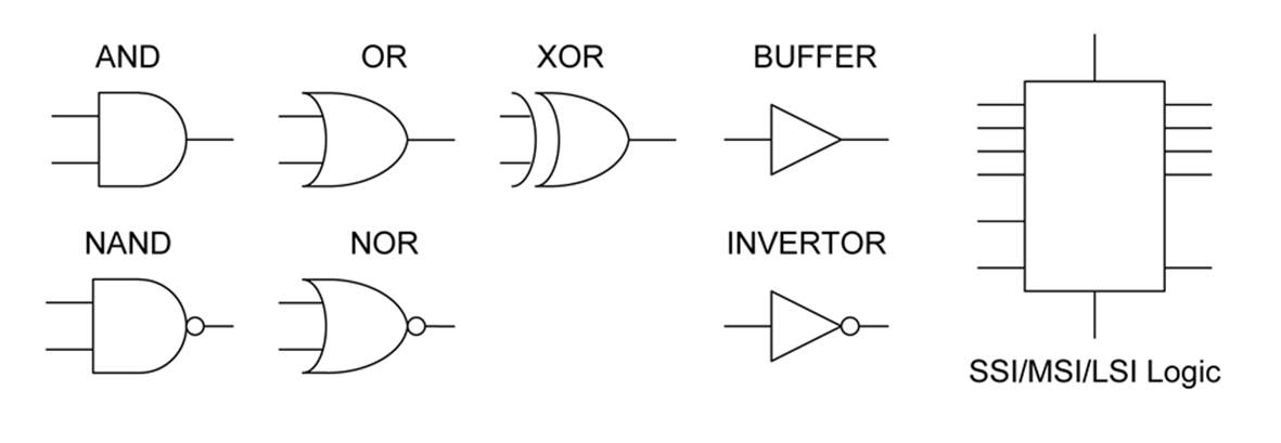
Figure B-11. Digital ICs
The small “bubbles” used with digital logic symbols (as shown in Figure B-11) indicate inversion; that is, if a logical true (1) encounters a bubble, it is inverted and becomes a logical false (0), and vice versa. See Chapter 9 for more on digital logic.
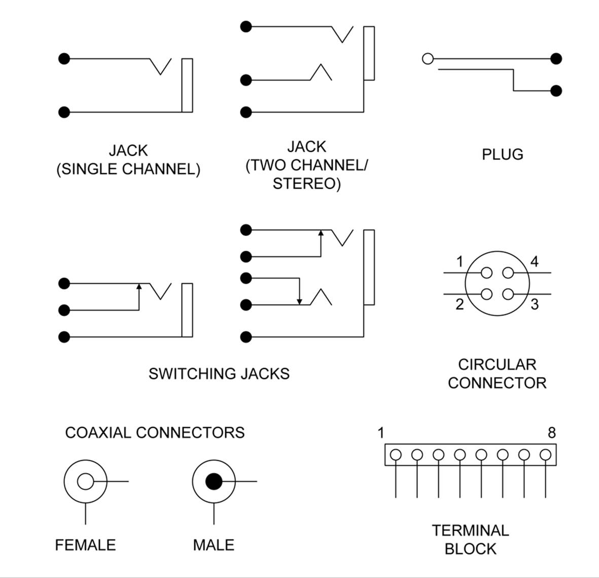
Figure B-12. Connectors
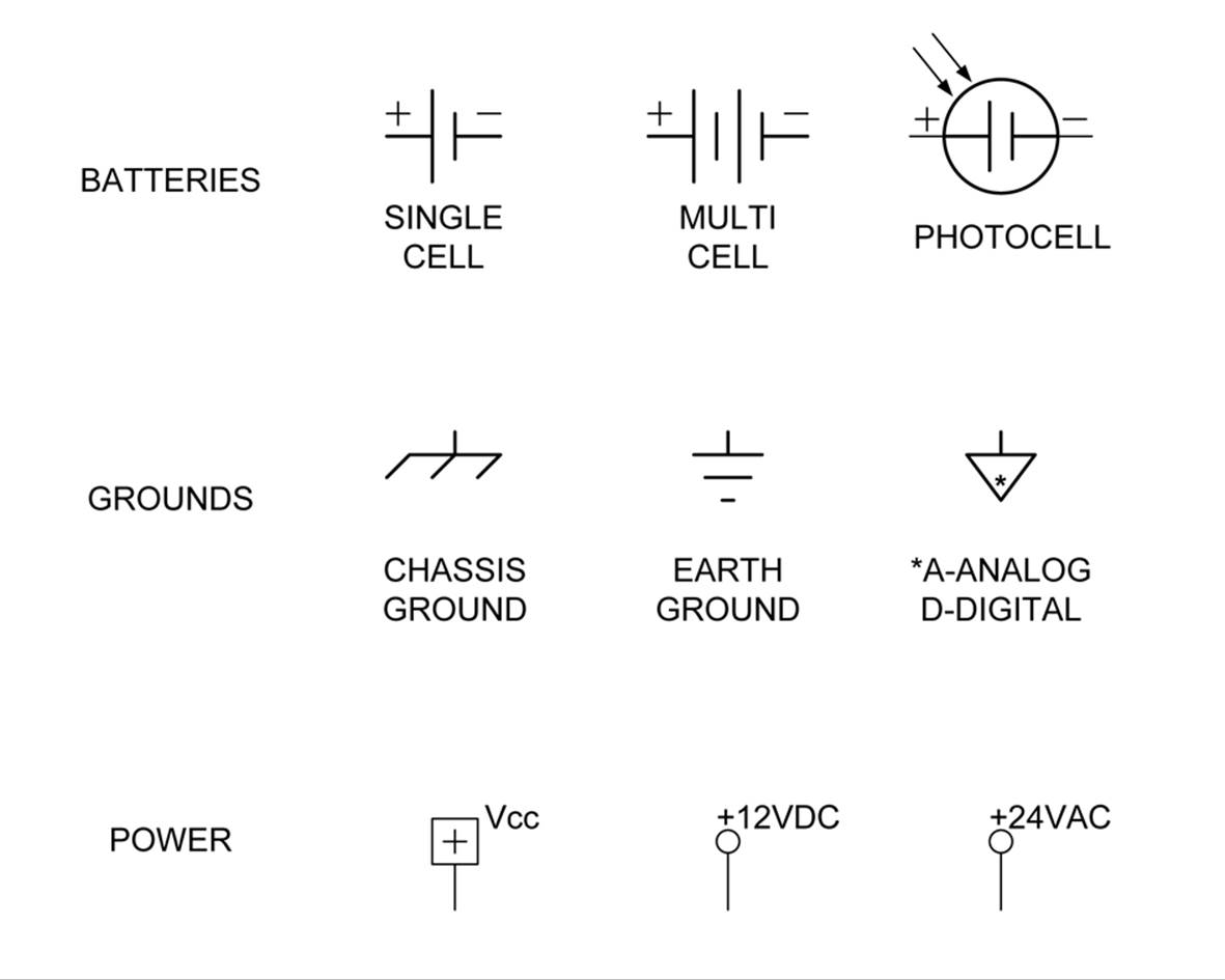
Figure B-13. Power and ground symbols
Schematic Capture and EDA Tools
There are multiple ways to create a schematic, ranging from a rough sketch on a napkin or the back of an envelope to a 17-inch × 22-inch piece of art generated with an EDA (electronic design automation) package and a special plotter or printer. For most people, the first, and least expensive, step is the notepad and a pencil.
Although just about any piece of paper will do, engineering notepads are readily available with 1/4-inch and 1/5-inch grids. They usually have a greenish tint, with heavy ruling on the back side that is faintly visible from the front. Grab a pencil (and perhaps a ruler), and you are ready to capture your design ideas on paper. While a nice schematic capture package can create pretty drawings, in reality, you can usually whip up a decent simple schematic with a pencil quicker than with a software package.
But when you need to be able to automatically generate a parts list, create a connection list (a netlist), export an EDIF file, or do a design rules check, then software is the way to go. A schematic created with an EDA tool also has the benefit of serving as the input to a PCB layout tool.
Software for electronics design comes in multiple forms. Some applications are intended for schematic capture only, others do PCB layouts, and some incorporate all (or most) of the tools necessary for end-to-end design of an electronic system. These full-up tool suites are known aselectronic design automation systems, and they can handle everything from schematic capture to circuit layout. Some are also capable of 3D physical modeling and even thermal analysis.
Several well-known, high-end EDA systems are available for electronics schematic capture and other design tasks. Products from Altium, Cadence (Orcad), and Mentor Graphics (PADS) are all excellent packages, but the price of these products can put them out of reach for an individual, a small makerspace, or even many small companies. Viable alternatives include open source programs (gEDA, KiCad, XCircuit), free limited-capability tools (EAGLE), and low-cost drawing tools (Visio).
Chapter 15 describes PCB layout concepts, which is a major part of the EAGLE, gEDA, and KiCad tools. XCircuit is intended as a schematic capture only, and Visio is a general-purpose line-art graphics tool with the capability of creating schematics from primitive graphic elements or from predefined stencils. Each is described briefly in the following sections, along with a link to follow for more information or to download the software.
Open Source and Commercial Tools for Schematic Capture
This section describes some of the most common and popular tools for schematic capture.
EAGLE
The EAGLE EDA tool from CadSoft (shown in Figure B-14) contains a schematic capture tool, a layout editor, autorouter, and library modules with symbols and layout templates for a variety of common parts. Interestingly, the entire tool package is installed on the target platform, but when EAGLE starts, it will ask if the user has a license. If not, then EAGLE can run as freeware mode with the following limited capabilities:
§ Maximum PCB area is 4 × 3.2 inches (100 × 80 millimeters).
§ A PCB can only have two layers (top and bottom).
§ A schematic can have only a single sheet (1 page).
If you purchase a license, it will unlock more of the capabilities of EAGLE, but for many small designs, these limitations are not a major impediment (the entire design for a Arduino board will fit on a single sheet). The EAGLE EDA tool will run on Linux, Windows, and Mac OS X.
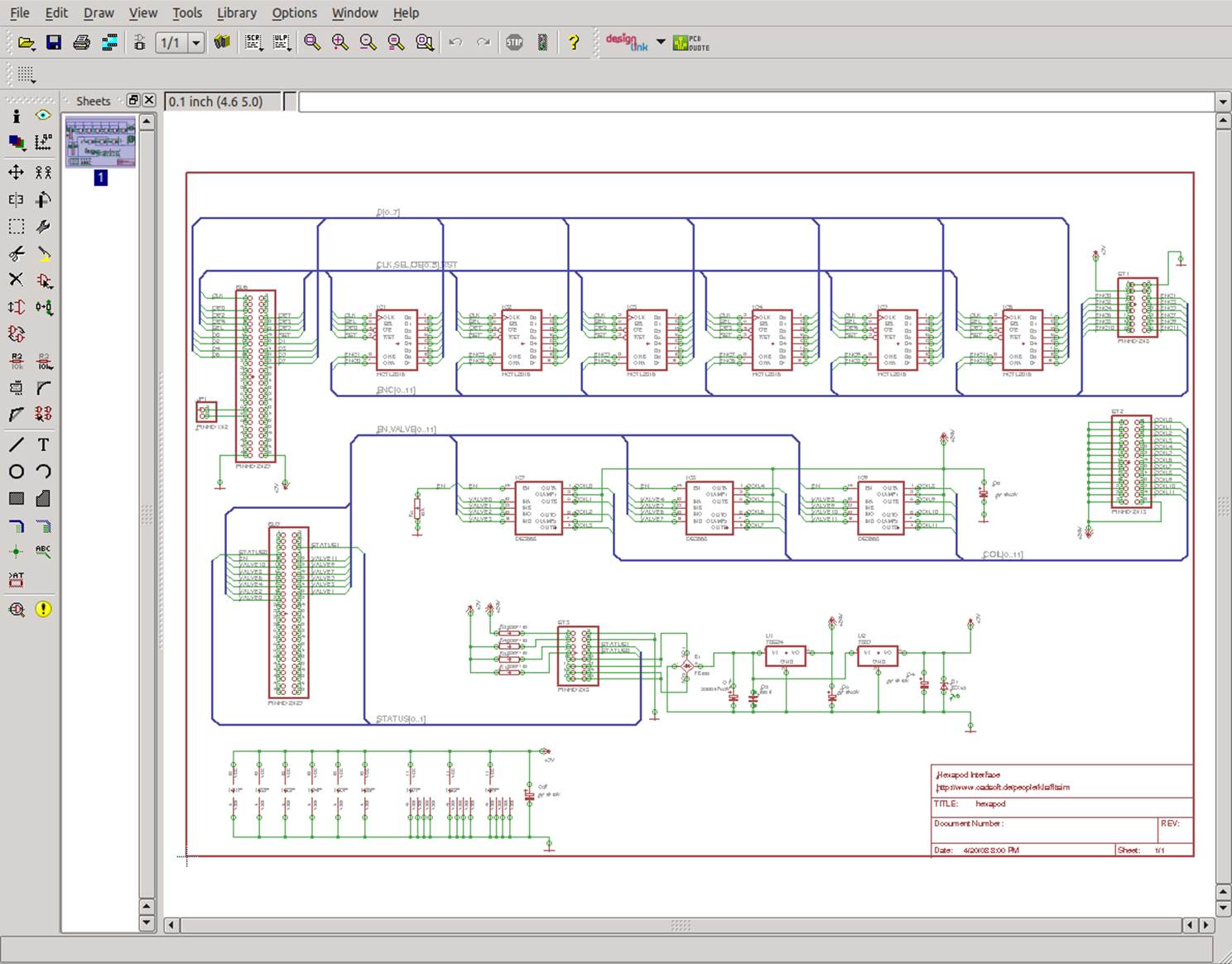
Figure B-14. The main EAGLE schematic capture interface
For more information about EAGLE and to download the free version, see CadSoft’s website.
gEDA
Started in the 1990s, gEDA (shown in Figure B-15) has evolved into a complete suite of open source EDA tools. It includes schematic capture, behavior simulation, PCB layout, and BOM and netlist generation.
Schematics created using the schematic capture tool gschem can be printed to a PostScript file for printing or further conversion to other output formats (similar to how XCircuit works). gschem can also be used to create custom schematic symbols and block diagrams.
gEDA is a set of GNU/Linux or Unix-native programs, and there is no officially supported Windows version. The website does mention a way to build the gEDA tools for Windows using the GTK+ libraries, however. gEDA is available for most major Linux distributions as a set of installable packages.
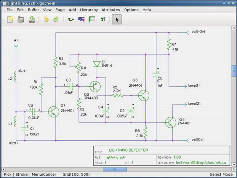
Figure B-15. The gEDA schematic capture tool, gschem
You can find more information about the gEDA projects and tools at the gEDA project home page.
KiCad
KiCad (shown in Figure B-16) is a GPL open source EDA software suite that consists of a schematic capture tool, a printed circuit board layout editor, a Gerber PCB file viewer, and a package footprint (physical form factor) tool. It also comes with a library of 3D models and can use an add-on rendering package to produce 3D CGI representations of what a finished PCB will look like.
KiCad runs on Windows, Linux, and Mac OS X, and is available for most major Linux distributions as an installable package.
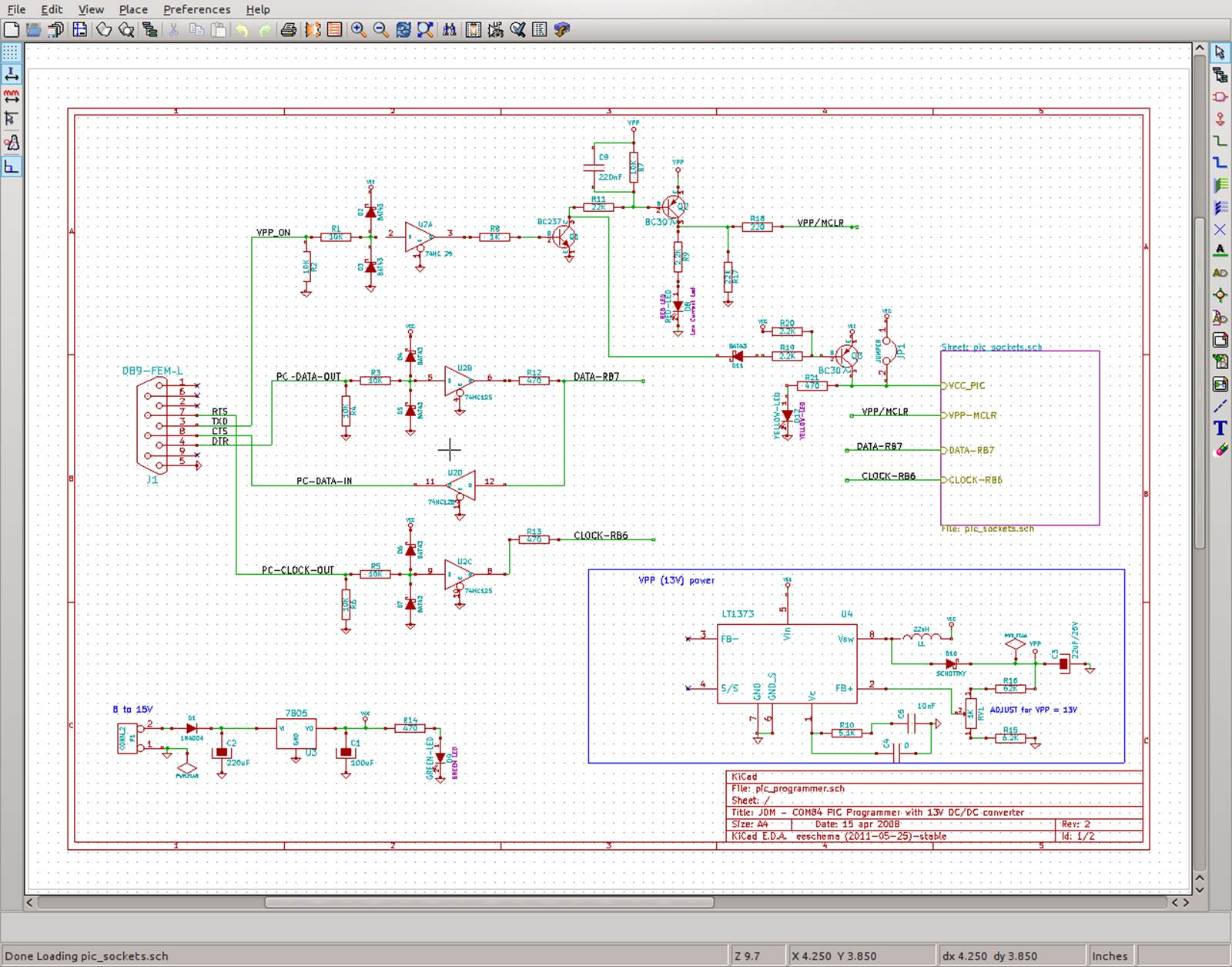
Figure B-16. The KiCad EDA tool
For more information, see the KiCad home page.
Visio
For those of you who are saying, “Wait! What? Visio?” well, you might want to take a second look. It’s actually a powerful graphics tool with a many more capabilities than are readily apparent on the surface, and it does more than create simple block diagrams and flow charts (see Figure B-17). Another useful feature of Visio is that it will integrate directly with Microsoft Word, and it can generate a huge variety of output file formats (DXF, JPG, PNG, SVG, TIFF, etc.).
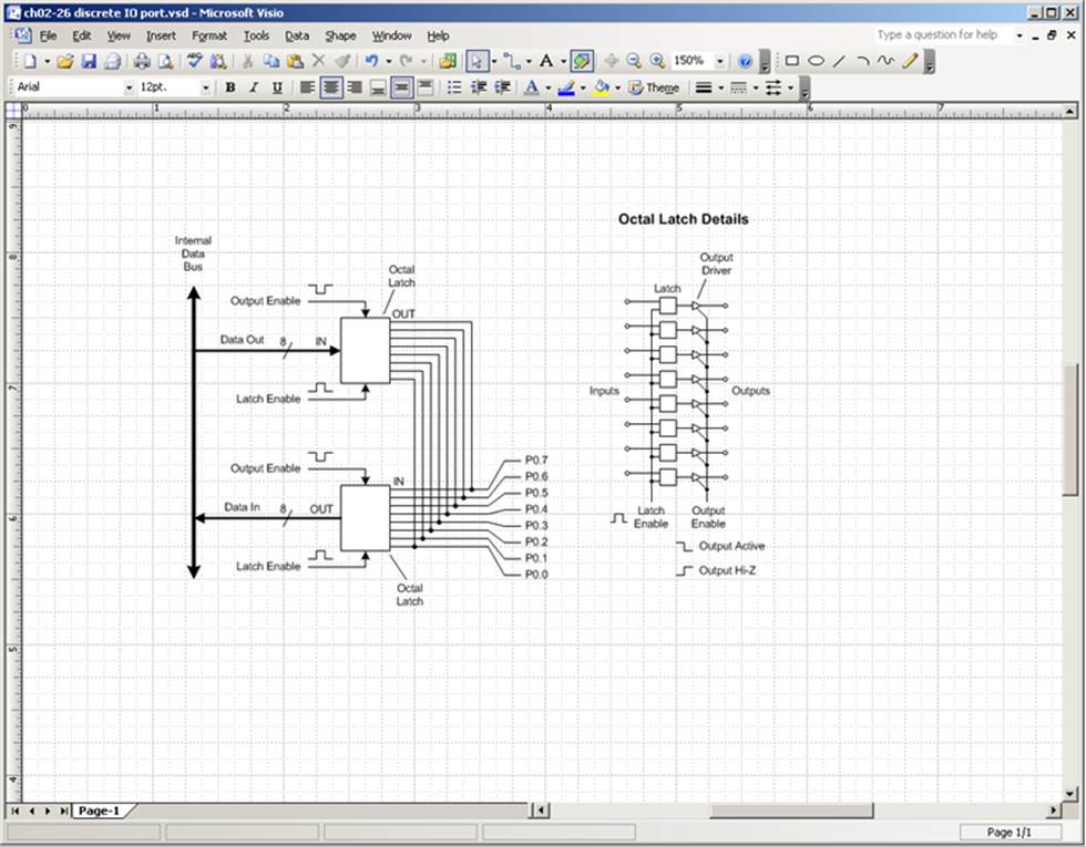
Figure B-17. Example Visio diagram
If you do elect to use Visio, you will, of course, need to use Windows. I would also suggest the technical version of Visio, which comes with various useful stencils (templates) that would otherwise have to be created by hand. A suite of electronics symbols for Visio, based on the symbology found in the 2008 ARRL handbook, is available from RF CAFE.
The technical edition of Visio also has a set of engineering stencils that include various schematic symbols.
XCircuit
The XCircuit application is intended for producing publication-quality schematics, although it can also be used as a generic line-art program for other applications. XCircuit is a not a full-up EDA tool, nor is it intended to be. But what it does, it does pretty well. Figure B-18 is a screenshot of XCircuit showing the contents of one of the libraries supplied with the tool.
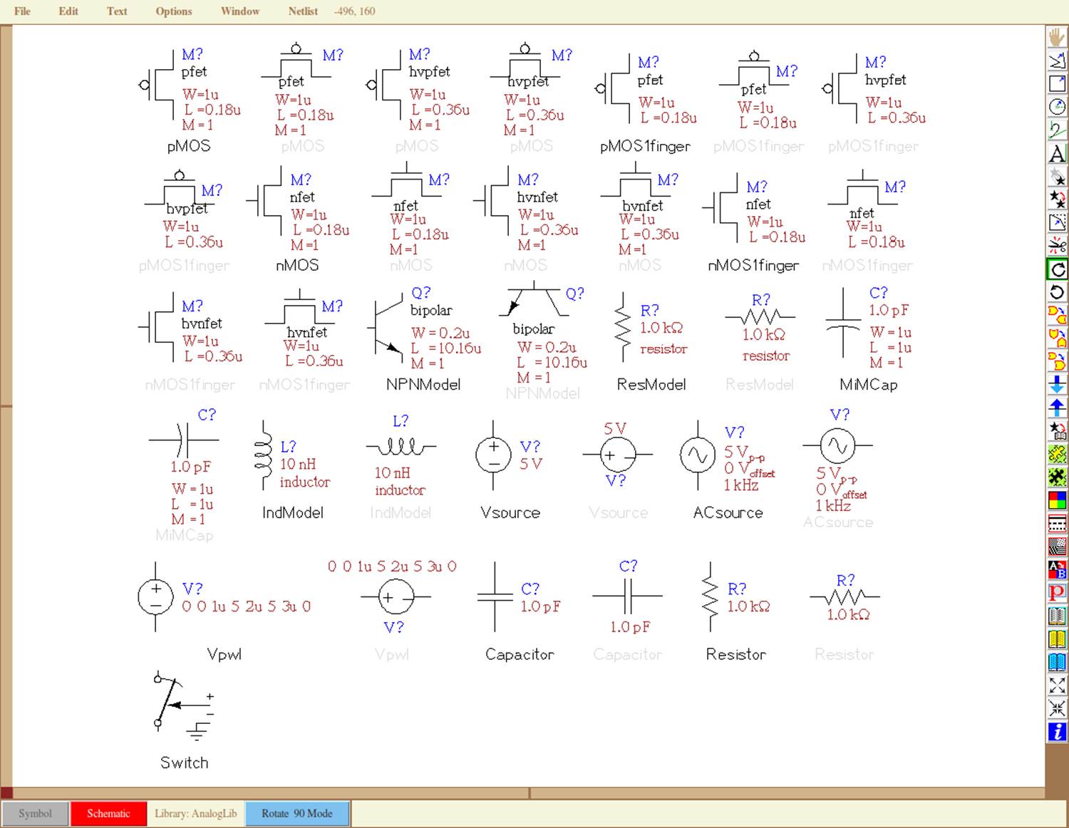
Figure B-18. The XCircuit schematic capture tool
The output of XCircuit is PostScript—nothing else. Schematics created with XCircuit can be imported into any word processor or graphics tool that can deal with PostScript. The XCircuit program itself is programmable using the Tcl language, so you can add functionality to meet your own specific needs.
For more information, see the XCircuit home page.
Other Open Source Schematic Capture Tools
You might also want to check out the following tools, which might appeal to you more than the ones highlighted previously. Each has its own unique set of strengths and weaknesses, which you’ll want to research yourself:
§ Oregano
§ Open Schematic Capture (OSC)
§ Itecad
§ TinyCAD
All materials on the site are licensed Creative Commons Attribution-Sharealike 3.0 Unported CC BY-SA 3.0 & GNU Free Documentation License (GFDL)
If you are the copyright holder of any material contained on our site and intend to remove it, please contact our site administrator for approval.
© 2016-2026 All site design rights belong to S.Y.A.