Computer Organization and Design (2016)
APPENDIX D
Mapping Control to Hardware
Abstract
This chapter shows the implementation of a control that has a combinational part that lacks state and a sequential control unit that handles sequencing and the main control in a multicycle design. To do this, it shows an implementation both for a ROM and a PLA, as well as an alternative method of implementation that computes the nextstate function by using a counter that increments the current state to determine the next state. The chapter also explains that when the next state doesn’t follow sequentially, other logic is used to determine the state: it explores this type of implementation and shows how it can be used to implement finite-state control. The chapter concludes by showing how a microprogram representation of sequential control is translated to control logic.
Keywords
combinational control unit, finite-state machine, nextstate function, sequencer, mircroprogram
A custom format such as this is slave to the architecture of the hardware and the instruction set it serves. The format must strike a proper compromise between ROM size, ROM-output decoding, circuitry size, and machine execution rate.
Jim McKevit, et al. 8086 design report, 1997
D.1 Introduction
D.2 Implementing Combinational Control Units
D.3 Implementing Finite-State Machine Control
D.4 Implementing the NextState Function with a Sequencer
D.5 Translating a Microprogram to Hardware
D.6 Concluding Remarks
D.7 Exercises
D.1 Introduction
Control typically has two parts: a combinational part that lacks state and a sequential control unit that handles sequencing and the main control in a multicycle design. Combinational control units are often used to handle part of the decode and control process. The ALU control in Chapter 4 is such an example. A single-cycle implementation like that in Chapter 4 can also use a combinational controller, since it does not require multiple states. Section D.2 examines the implementation of these two combinational units from the truth tables of Chapter 4.
Since sequential control units are larger and often more complex, there are a wider variety of techniques for implementing a sequential control unit. The usefulness of these techniques depends on the complexity of the control, characteristics such as the average number of next states for any given state, and the implementation technology.
The most straightforward way to implement a sequential control function is with a block of logic that takes as inputs the current state and the opcode field of the Instruction register and produces as outputs the datapath control signals and the value of the next state. The initial representation may be either a finite-state diagram or a microprogram. In the latter case, each microinstruction represents a state.
In an implementation using a finite-state controller, the nextstate function will be computed with logic. Section D.3 constructs such an implementation both for a ROM and a PLA.
An alternative method of implementation computes the nextstate function by using a counter that increments the current state to determine the next state. When the next state doesn’t follow sequentially, other logic is used to determine the state. Section D.4 explores this type of implementation and shows how it can be used to implement finite-state control.
In Section D.5, we show how a microprogram representation of sequential control is translated to control logic.
D.2 Implementing Combinational Control Units
In this section, we show how the ALU control unit and main control unit for the single clock design are mapped down to the gate level. With modern computer-aided design (CAD) systems, this process is completely mechanical. The examples illustrate how a CAD system takes advantage of the structure of the control function, including the presence of don’t-care terms.
Mapping the ALU Control Function to Gates
Figure D.2.1 shows the truth table for the ALU control function that was developed in Section 4.3. A logic block that implements this ALU control function will have four distinct outputs (called Operation3, Operation2, Operation1, and Operation0), each corresponding to one of the four bits of the ALU control in the last column of Figure D.2.1. The logic function for each output is constructed by combining all the truth table entries that set that particular output. For example, the low-order bit of the ALU control (Operation0) is set by the last two entries of the truth table in Figure D.2.1. Thus, the truth table for Operation0 will have these two entries.
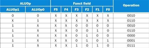
FIGURE D.2.1 The truth table for the 4 ALU control bits (called Operation) as a function of the ALUOp and function code field.
This table is the same as that shown in Figure 4.13.
Figure D.2.2 shows the truth tables for each of the four ALU control bits. We have taken advantage of the common structure in each truth table to incorporate additional don’t cares. For example, the five lines in the truth table of Figure D.2.1 that set Operation1 are reduced to just two entries in Figure D.2.2. A logic minimization program will use the don’t-care terms to reduce the number of gates and the number of inputs to each gate in a logic gate realization of these truth tables.
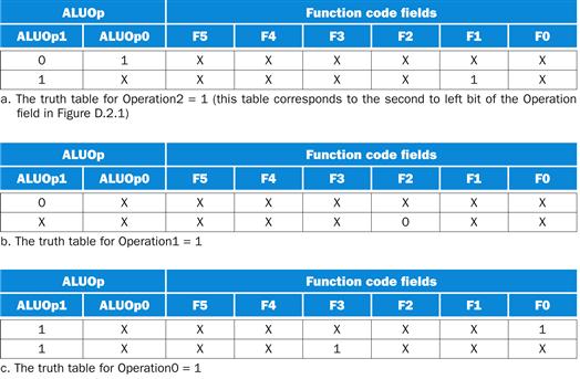
FIGURE D.2.2 The truth tables for three ALU control lines.
Only the entries for which the output is 1 are shown. The bits in each field are numbered from right to left starting with 0; thus F5 is the most significant bit of the function field, and F0 is the least significant bit. Similarly, the names of the signals corresponding to the 4-bit operation code supplied to the ALU are Operation3, Operation2, Operation1, and Operation0 (with the last being the least significant bit). Thus the truth table above shows the input combinations for which the ALU control should be 0010, 0001, 0110, or 0111 (the other combinations are not used). The ALUOp bits are named ALUOp1 and ALUOp0. The three output values depend on the 2-bit ALUOp field and, when that field is equal to 10, the 6-bit function code in the instruction. Accordingly, when the ALUOp field is not equal to 10, we don’t care about the function code value (it is represented by an X). There is no truth table for when Operation3=1 because it is always set to 0 in Figure D.2.1. See Appendix B for more background on don’t cares.
A confusing aspect of Figure D.2.2 is that there is no logic function for Operation3. That is because this control line is only used for the NOR operation, which is not needed for the MIPS subset in Figure 4.12.
From the simplified truth table in Figure D.2.2, we can generate the logic shown in Figure D.2.3, which we call the ALU control block. This process is straightforward and can be done with a CAD program. An example of how the logic gates can be derived from the truth tables is given in the legend to Figure D.2.3.
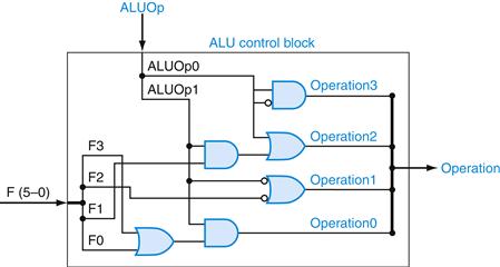
FIGURE D.2.3 The ALU control block generates the four ALU control bits, based on the function code and ALUOp bits.
This logic is generated directly from the truth table in Figure D.2.2. Only four of the six bits in the function code are actually needed as inputs, since the upper two bits are always don’t cares. Let’s examine how this logic relates to the truth table of Figure D.2.2. Consider the Operation2 output, which is generated by two lines in the truth table for Operation2. The second line is the AND of two terms (F1 = 1 and ALUOp1 = 1); the top two-input AND gate corresponds to this term. The other term that causes Operation2 to be asserted is simply ALUOp0. These two terms are combined with an OR gate whose output is Operation2. The outputs Operation0 and Operation1 are derived in similar fashion from the truth table. Since Operation3 is always 0, we connect a signal and its complement as inputs to an AND gate to generate 0.
This ALU control logic is simple because there are only three outputs, and only a few of the possible input combinations need to be recognized. If a large number of possible ALU function codes had to be transformed into ALU control signals, this simple method would not be efficient. Instead, you could use a decoder, a memory, or a structured array of logic gates. These techniques are described in Appendix B, and we will see examples when we examine the implementation of the multicycle controller in Section D.3.
Elaboration
In general, a logic equation and truth table representation of a logic function are equivalent. (We discuss this in further detail in Appendix (B) However, when a truth table only specifies the entries that result in nonzero outputs, it may not completely describe the logic function. A full truth table completely indicates all don’t-care entries. For example, the encoding 11 for ALUOp always generates a don’t care in the output. Thus a complete truth table would have XXX in the output portion for all entries with 11 in the ALUOp field. These don’t-care entries allow us to replace the ALUOp field 10 and 01 with 1X and X1, respectively. Incorporating the don’t-care terms and minimizing the logic is both complex and error-prone and, thus, is better left to a program.
Mapping the Main Control Function to Gates
Implementing the main control function with an unstructured collection of gates, as we did for the ALU control, is reasonable because the control function is neither complex nor large, as we can see from the truth table shown in Figure D.2.4. However, if most of the 64 possible opcodes were used and there were many more control lines, the number of gates would be much larger and each gate could have many more inputs.
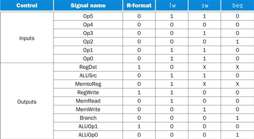
FIGURE D.2.4 The control function for the simple one-clock implementation is completely specified by this truth table.
This table is the same as that shown in Figure 4.22.
Since any function can be computed in two levels of logic, another way to implement a logic function is with a structured two-level logic array. Figure D.2.5 shows such an implementation. It uses an array of AND gates followed by an array of OR gates. This structure is called a programmable logic array (PLA). A PLA is one of the most common ways to implement a control function. We will return to the topic of using structured logic elements to implement control when we implement the finite-state controller in the next section.
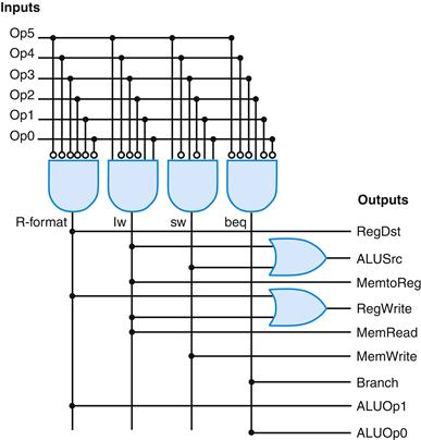
FIGURE D.2.5 The structured implementation of the control function as described by the truth table in Figure D.2.4.
The structure, called a programmable logic array (PLA), uses an array of AND gates followed by an array of OR gates. The inputs to the AND gates are the function inputs and their inverses (bubbles indicate inversion of a signal). The inputs to the OR gates are the outputs of the AND gates (or, as a degenerate case, the function inputs and inverses). The output of the OR gates is the function outputs.
D.3 Implementing Finite-State Machine Control
To implement the control as a finite-state machine, we must first assign a number to each of the 10 states; any state could use any number, but we will use the sequential numbering for simplicity. Figure D.3.1shows the finite-state diagram. With 10 states, we will need 4 bits to encode the state number, and we call these state bits S3, S2, S1, and S0. The current-state number will be stored in a state reg ister, as shown in Figure D.3.2. If the states are assigned sequentially, state i is encoded using the state bits as the binary number i. For example, state 6 is encoded as 0110two or S3 = 0, S2 = 1, S1 = 1, S0 = 0, which can also be written as
![]()
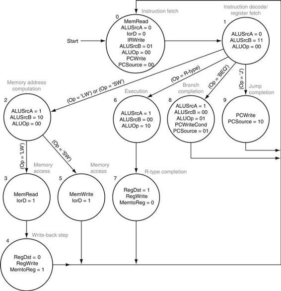
FIGURE D.3.1 The finite-state diagram for multicycle control.
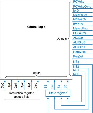
FIGURE D.3.2 The control unit for MIPS will consist of some control logic and a register to hold the state.
The state register is written at the active clock edge and is stable during the clock cycle
The control unit has outputs that specify the next state. These are written into the state register on the clock edge and become the new state at the beginning of the next clock cycle following the active clock edge. We name these outputs NS3, NS2, NS1, and NS0. Once we have determined the number of inputs, states, and out puts, we know what the basic outline of the control unit will look like, as we show in Figure D.3.2.
The block labeled “control logic” in Figure D.3.2 is combinational logic. We can think of it as a big table giving the value of the outputs in terms of the inputs. The logic in this block implements the two different parts of the finite-state machine. One part is the logic that determines the setting of the datapath control outputs, which depend only on the state bits. The other part of the control logic implements the nextstate function; these equations determine the values of the nextstate bits based on the current-state bits and the other inputs (the 6-bit opcode).
Figure D.3.3 shows the logic equations: the top portion shows the outputs, and the bottom portion shows the nextstate function. The values in this table were determined from the state diagram in Figure D.3.1. Whenever a control line is active in a state, that state is entered in the second column of the table. Likewise, the nextstate entries are made whenever one state is a successor to another.
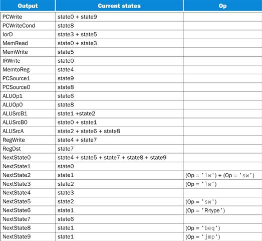
FIGURE D.3.3 The logic equations for the control unit shown in a shorthand form.
Remember that “+” stands for OR in logic equations. The state inputs and NextState outputs must be expanded by using the state encoding. Any blank entry is a don’t care.
In Figure D.3.3, we use the abbreviation stateN to stand for current state N. Thus, stateN is replaced by the term that encodes the state number N. We use NextStateN to stand for the setting of the nextstate outputs to N. This output is implemented using the nextstate outputs (NS). When NextStateN is active, the bits NS[3–0] are set corresponding to the binary version of the value N. Of course, since a given nextstate bit is activated in multiple next states, the equation for each state bit will be the OR of the terms that activate that signal. Likewise, when we use a term such as (Op = ‘lw’), this corresponds to an AND of the opcode inputs that specifies the encoding of the opcode lw in 6 bits, just as we did for the simple control unit in the previous section of this chapter. Translating the entries in Figure D.3.3 into logic equations for the outputs is straight forward.
Logic Equations for NextState Outputs
Example
Give the logic equation for the low-order nextstate bit, NS0.
Answer
The nextstate bit NS0 should be active whenever the next state has NS0 = 1 in the state encoding. This is true for NextState1, NextState3, NextState5, NextState7, and NextState9. The entries for these states in Figure D.3.3 supply the conditions when these nextstate values should be active. The equation for each of these next states is given below. The first equation states that the next state is 1 if the current state is 0; the current state is 0 if each of the state input bits is 0, which is what the rightmost product term indicates.
![]()
![]()
![]()
NextState7 = State6 = S3 · S2 · S1 · S0
![]()
NS0 is the logical sum of all these terms.
As we have seen, the control function can be expressed as a logic equation for each output. This set of logic equations can be implemented in two ways: corresponding to a complete truth table, or corresponding to a two-level logic structure that allows a sparse encoding of the truth table. Before we look at these implementations, let’s look at the truth table for the complete control function.
It is simplest if we break the control function defined in Figure D.3.3 into two parts: the nextstate outputs, which may depend on all the inputs, and the control signal outputs, which depend only on the current-state bits. Figure D.3.4 shows the truth tables for all the datapath control signals. Because these signals actually depend only on the state bits (and not the opcode), each of the entries in a table in Figure D.3.4 actually represents 64 (= 26) entries, with the 6 bits named Op having all possible values; that is, the Op bits are don’t-care bits in determining the data path control outputs. Figure D.3.5 shows the truth table for the nextstate bits NS[3–0], which depend on the state input bits and the instruction bits, which supply the opcode.
Elaboration
There are many opportunities to simplify the control function by observing similarities among two or more control signals and by using the semantics of the implementation. For example, the signals PCWriteCond, PCSource0, and ALUOp0 are all asserted in exactly one state, state 8. These three control signals can be replaced by a single signal.
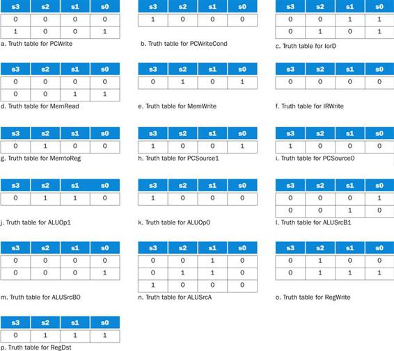
FIGURE D.3.4 The truth tables are shown for the 16 datapath control signals that depend only on the current-state input bits, which are shown for each table.
Each truth table row corresponds to 64 entries: one for each possible value of the six Op bits. Notice that some of the outputs are active under nearly the same circumstances. For example, in the case of PCWriteCond, PCSource0, and ALUOp0, these signals are active only in state 8 (see b, i, and k). These three signals could be replaced by one signal. There are other opportunities for reducing the logic needed to implement the control function by taking advantage of further similarities in the truth tables.
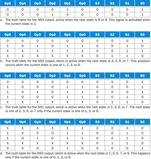
FIGURE D.3.5 The four truth tables for the four nextstate output bits (NS[3–0]).
The nextstate outputs depend on the value of Op[5-0], which is the opcode field, and the current state, given by S[3–0]. The entries with X are don’t-care terms. Each entry with a don’t-care term corresponds to two entries, one with that input at 0 and one with that input at 1. Thus an entry with n don’t-care terms actually corresponds to 2n truth table entries.
A ROM Implementation
Probably the simplest way to implement the control function is to encode the truth tables in a read-only memory (ROM). The number of entries in the memory for the truth tables of Figures D.3.4 and D.3.5 is equal to all possible values of the inputs (the 6 opcode bits plus the 4 state bits), which is 2# inputs = 210 = 1024. The inputs to the control unit become the address lines for the ROM, which implements the control logic block that was shown in Figure D.3.2. The width of each entry (or word in the memory) is 20 bits, since there are 16 datapath control outputs and 4 nextstate bits. This means the total size of the ROM is 210 × 20 = 20 Kbits.
The setting of the bits in a word in the ROM depends on which outputs are active in that word. Before we look at the control words, we need to order the bits within the control input (the address) and output words (the contents), respectively. We will number the bits using the order in Figure D.3.2, with the nextstate bits being the low-order bits of the control word and the current-state input bits being the low-order bits of the address. This means that the PCWrite output will be the high-order bit (bit 19) of each memory word, and NS0 will be the low-order bit. The high-order address bit will be given by Op5, which is the high-order bit of the instruction, and the low-order address bit will be given by S0.
We can construct the ROM contents by building the entire truth table in a form where each row corresponds to one of the 2n unique input combinations, and a set of columns indicates which outputs are active for that input combination. We don’t have the space here to show all 1024 entries in the truth table. However, by separating the datapath control and nextstate outputs, we do, since the datapath control outputs depend only on the current state. The truth table for the datapath control outputs is shown in Figure D.3.6. We include only the encodings of the state inputs that are in use (that is, values 0 through 9 corresponding to the 10 states of the state machine).
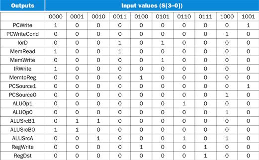
FIGURE D.3.6 The truth table for the 16 datapath control outputs, which depend only on the state inputs.
The values are determined from Figure D.3.4. Although there are 16 possible values for the 4-bit state field, only ten of these are used and are shown here. The ten possible values are shown at the top; each column shows the setting of the datapath control outputs for the state input value that appears at the top of the column. For example, when the state inputs are 0011 (state 3), the active datapath control outputs are IorD or MemRead.
The truth table in Figure D.3.6 directly gives the contents of the upper 16 bits of each word in the ROM. The 4-bit input field gives the low-order 4 address bits of each word, and the column gives the contents of the word at that address.
If we did show a full truth table for the datapath control bits with both the state number and the opcode bits as inputs, the opcode inputs would all be don’t cares. When we construct the ROM, we cannot have any don’t cares, since the addresses into the ROM must be complete. Thus, the same datapath control outputs will occur many times in the ROM, since this part of the ROM is the same whenever the state bits are identical, independent of the value of the opcode inputs.
Control ROM Entries
Example
For what ROM addresses will the bit corresponding to PCWrite, the high bit of the control word, be 1?
Answer
PCWrite is high in states 0 and 9; this corresponds to addresses with the 4 low-order bits being either 0000 or 1001. The bit will be high in the memory word independent of the inputs Op[5–0], so the addresses with the bit high are 000000000, 0000001001, 0000010000, 0000011001, … , 1111110000, 1111111001. The general form of this is XXXXXX0000 or XXXXXX1001, where XXXXXX is any combination of bits, and corresponds to the 6-bit opcode on which this output does not depend.
We will show the entire contents of the ROM in two parts to make it easier to show. Figure D.3.7 shows the upper 16 bits of the control word; this comes directly from Figure D.3.6. These datapath control outputs depend only on the state inputs, and this set of words would be duplicated 64 times in the full ROM, as we discussed above. The entries corresponding to input values 1010 through 1111 are not used, so we do not care what they contain.
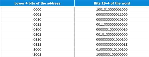
FIGURE D.3.7 The contents of the upper 16 bits of the ROM depend only on the state inputs.
These values are the same as those in Figure D.3.6, simply rotated 90°. This set of control words would be duplicated 64 times for every possible value of the upper six bits of the address.
Figure D.3.8 shows the lower four bits of the control word corresponding to the nextstate outputs. The last column of the table in Figure D.3.8 corresponds to all the possible values of the opcode that do not match the specified opcodes. In state 0, the next state is always state 1, since the instruction was still being fetched. After state 1, the opcode field must be valid. The table indicates this by the entries marked illegal; we discuss how to deal with these illegal opcodes in Section 4.9.
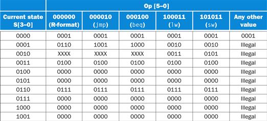
FIGURE D.3.8 This table contains the lower 4 bits of the control word (the NS outputs), which depend on both the state inputs, S[3–0], and the opcode, Op[5–0], which correspond to the instruction opcode.
These values can be determined from Figure D.3.5. The opcode name is shown under the encoding in the heading. The four bits of the control word whose address is given by the current-state bits and Op bits are shown in each entry. For example, when the state input bits are 0000, the output is always 0001, independent of the other inputs; when the state is 2, the next state is don’t care for three of the inputs, 3 for lw, and 5 for sw. Together with the entries in Figure D.3.7, this table specifies the contents of the control unit ROM. For example, the word at address 1000110001 is obtained by finding the upper 16 bits in the table in Figure D.3.7 using only the state input bits (0001) and concatenating the lower four bits found by using the entire address (0001 to find the row and 100011 to find the column). The entry from Figure D.3.7 yields 0000000000011000, while the appropriate entry in the table immediately above is 0010. Thus the control word at address 1000110001 is 00000000000110000010. The column labeled “Any other value” applies only when the Op bits do not match one of the specified opcodes.
Not only is this representation as two separate tables a more compact way to show the ROM contents, it is also a more efficient way to implement the ROM. The majority of the outputs (16 of 20 bits) depends only on 4 of the 10 inputs. The num ber of bits in total when the control is implemented as two separate ROMs is 24 × 16 + 210 × 4 = 256 + 4096 = 4.3 Kbits, which is about one-fifth of the size of a single ROM, which requires 210 × 20 = 20 Kbits. There is some overhead associated with any structured-logic block, but in this case the additional overhead of an extra ROM would be much smaller than the savings from splitting the single ROM.
Although this ROM encoding of the control function is simple, it is wasteful, even when divided into two pieces. For example, the values of the Instruction register inputs are often not needed to determine the next state. Thus, the nextstate ROM has many entries that are either duplicated or are don’t care. Consider the case when the machine is in state 0: there are 26 entries in the ROM (since the opcode field can have any value), and these entries will all have the same contents (namely, the control word 0001). The reason that so much of the ROM is wasted is that the ROM implements the complete truth table, providing the opportunity to have a different output for every combination of the inputs. But most combinations of the inputs either never happen or are redundant!
A PLA Implementation
We can reduce the amount of control storage required at the cost of using more complex address decoding for the control inputs, which will encode only the input combinations that are needed. The logic structure most often used to do this is a programmed logic array (PLA), which we mentioned earlier and illustrated in Figure D.2.5. In a PLA, each output is the logical OR of one or more minterms. A minterm, also called a product term, is simply a logical AND of one or more inputs. The inputs can be thought of as the address for indexing the PLA, while the minterms select which of all possible address combinations are interesting. A minterm corresponds to a single entry in a truth table, such as those in Figure D.3.4, including possible don’t-care terms. Each output consists of an OR of these minterms, which exactly corresponds to a complete truth table. However, unlike a ROM, only those truth table entries that produce an active output are needed, and only one copy of each minterm is required, even if the minterm contains don’t cares. Figure D.3.9 shows the PLA that implements this control function.
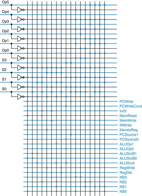
FIGURE D.3.9 This PLA implements the control function logic for the multicycle implementation.
The inputs to the control appear on the left and the outputs on the right. The top half of the figure is the AND plane that computes all the minterms. The minterms are carried to the OR plane on the vertical lines. Each colored dot corresponds to a signal that makes up the minterm carried on that line. The sum terms are computed from these minterms, with each gray dot representing the presence of the intersecting minterm in that sum term. Each output consists of a single sum term.
As we can see from the PLA in Figure D.3.9, there are 17 unique minterms—10 that depend only on the current state and 7 others that depend on a combination of the Op field and the current-state bits. The total size of the PLA is proportional to (#inputs × #product terms) + (#outputs × #product terms), as we can see symbolically from the figure. This means the total size of the PLA in Figure D.3.9 is proportional to (10 × 17) + (20 × 17) = 510. By comparison, the size of a single ROM is proportional to 20 Kb, and even the two-part ROM has a total of 4.3 Kb. Because the size of a PLA cell will be only slightly larger than the size of a bit in a ROM, a PLA will be a much more efficient implementation for this control unit.
Of course, just as we split the ROM in two, we could split the PLA into two PLAs: one with 4 inputs and 10 minterms that generates the 16 control outputs, and one with 10 inputs and 7 minterms that generates the 4 nextstate outputs. The first PLA would have a size proportional to (4 × 10) + (10 × 16) = 200, and the second PLA would have a size proportional to (10 × 7) + (4 × 7) = 98. This would yield a total size proportional to 298 PLA cells, about 55% of the size of a single PLA. These two PLAs will be considerably smaller than an implementation using two ROMs. For more details on PLAs and their implementation, as well as the refer ences for books on logic design, see® Appendix B.
D.4 Implementing the NextState Function with a Sequencer
Let’s look carefully at the control unit we built in the last section. If you examine the ROMs that implement the control in Figures D.3.7 and D.3.8, you can see that much of the logic is used to specify the nextstate function. In fact, for the implementation using two separate ROMs, 4096 out of the 4368 bits (94%) correspond to the nextstate function! Furthermore, imagine what the control logic would look like if the instruction set had many more different instruction types, some of which required many clocks to implement. There would be many more states in the finite-state machine. In some states, we might be branching to a large number of different states depending on the instruction type (as we did in state 1 of the finite-state machine in Figure D.3.1). However, many of the states would proceed in a sequential fashion, just as states 3 and 4 do in Figure D.3.1.
For example, if we included floating point, we would see a sequence of many states in a row that implement a multicycle floating-point instruction. Alternatively, consider how the control might look for a machine that can have multiple memory operands per instruction. It would require many more states to fetch multiple memory operands. The result of this would be that the control logic will be dominated by the encoding of the nextstate function. Furthermore, much of the logic will be devoted to sequences of states with only one path through them that look like states 2 through 4 in Figure D.3.1. With more instructions, these sequences will consist of many more sequentially numbered states than for our simple subset.
To encode these more complex control functions efficiently, we can use a control unit that has a counter to supply the sequential next state. This counter often eliminates the need to encode the nextstate function explicitly in the control unit. As shown in Figure D.4.1, an adder is used to increment the state, essentially turning it into a counter. The incremented state is always the state that follows in numerical order. However, the finite-state machine sometimes “branches.” For example, in state 1 of the finite-state machine (see Figure D.3.1), there are four possible next states, only one of which is the sequential next state. Thus, we need to be able to choose between the incremented state and a new state based on the inputs from the Instruction register and the current state. Each control word will include control lines that will determine how the next state is chosen.
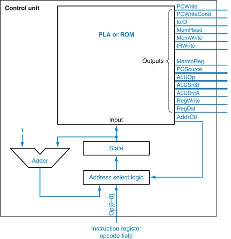
FIGURE D.4.1 The control unit using an explicit counter to compute the next state.
In this control unit, the next state is computed using a counter (at least in some states). By comparison, Figure D.3.2 encodes the next state in the control logic for every state. In this control unit, the signals labeled AddrCtl control how the next state is determined.
It is easy to implement the control output signal portion of the control word, since, if we use the same state numbers, this portion of the control word will look exactly like the ROM contents shown in Figure D.3.7. However, the method for selecting the next state differs from the nextstate function in the finite-state machine.
With an explicit counter providing the sequential next state, the control unit logic need only specify how to choose the state when it is not the sequentially following state. There are two methods for doing this. The first is a method we have already seen: namely, the control unit explicitly encodes the nextstate function. The difference is that the control unit need only set the nextstate lines when the designated next state is not the state that the counter indicates. If the number of states is large and the nextstate function that we need to encode is mostly empty, this may not be a good choice, since the resulting control unit will have lots of empty or redundant space. An alternative approach is to use separate external logic to specify the next state when the counter does not specify the state. Many control units, especially those that implement large instruction sets, use this approach, and we will focus on specifying the control externally.
Although the nonsequential next state will come from an external table, the control unit needs to specify when this should occur and how to find that next state. There are two kinds of “branching” that we must implement in the address select logic. First, we must be able to jump to one of a number of states based on the opcode portion of the Instruction register. This operation, called a dispatch, is usually implemented by using a set of special ROMs or PLAs included as part of the address selection logic. An additional set of control outputs, which we call AddrCtl, indicates when a dispatch should be done. Looking at the finite-state diagram (Figure D.3.1), we see that there are two states in which we do a branch based on a portion of the opcode. Thus we will need two small dis patch tables. (Alternatively, we could also use a single dispatch table and use the control bits that select the table as address bits that choose from which portion of the dispatch table to select the address.)
The second type of branching that we must implement consists of branching back to state 0, which initiates the execution of the next MIPS instruction. Thus there are four possible ways to choose the next state (three types of branches, plus incrementing the current-state number), which can be encoded in 2 bits. Let’s assume that the encoding is as follows:
|
AddrCtl value |
Action |
|
0 |
Set state to 0 |
|
1 |
Dispatch with ROM 1 |
|
2 |
Dispatch with ROM 2 |
|
3 |
Use the incremented state |
If we use this encoding, the address select logic for this control unit can be implemented as shown in Figure D.4.2.
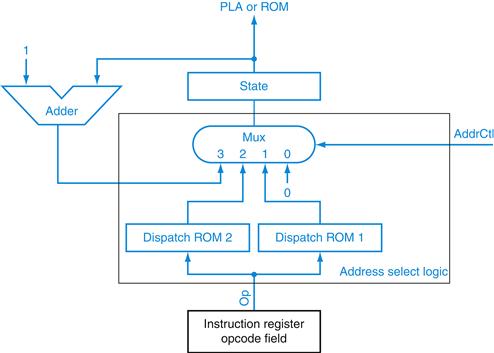
FIGURE D.4.2 This is the address select logic for the control unit of Figure D.4.1.
To complete the control unit, we need only specify the contents of the dispatch ROMs and the values of the address-control lines for each state. We have already specified the datapath control portion of the control word using the ROM con tents of Figure D.3.7 (or the corresponding portions of the PLA in Figure D.3.9). The nextstate counter and dispatch ROMs take the place of the portion of the control unit that was computing the next state, which was shown in Figure D.3.8. We are only implementing a portion of the instruction set, so the dispatch ROMs will be largely empty. Figure D.4.3 shows the entries that must be assigned for this subset.
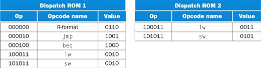
FIGURE D.4.3 The dispatch ROMs each have 26 = 64 entries that are 4 bits wide, since that is the number of bits in the state encoding.
This figure only shows the entries in the ROM that are of interest for this subset. The first column in each table indicates the value of Op, which is the address used to access the dispatch ROM. The second column shows the symbolic name of the opcode. The third column indicates the value at that address in the ROM.
Now we can determine the setting of the address selection lines (AddrCtl) in each control word. The table in Figure D.4.4 shows how the address control must be set for every state. This information will be used to specify the setting of the AddrCtl field in the control word associated with that state.
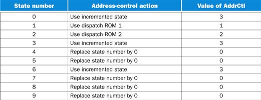
FIGURE D.4.4 The values of the address-control lines are set in the control word that corresponds to each state.
The contents of the entire control ROM are shown in Figure D.4.5. The total storage required for the control is quite small. There are 10 control words, each 18 bits wide, for a total of 180 bits. In addition, the two dispatch tables are 4 bits wide and each has 64 entries, for a total of 512 additional bits. This total of 692 bits beats the implementation that uses two ROMs with the nextstate function encoded in the ROMs (which requires 4.3 Kbits).
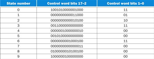
FIGURE D.4.5 The contents of the control memory for an implementation using an explicit counter.
The first column shows the state, while the second shows the datapath control bits, and the last column shows the address-control bits in each control word. Bits 17–2 are identical to those in Figure D.3.7.
Of course, the dispatch tables are sparse and could be more efficiently implemented with two small PLAs. The control ROM could also be replaced with a PLA.
Optimizing the Control Implementation
We can further reduce the amount of logic in the control unit by two different techniques. The first is logic minimization, which uses the structure of the logic equations, including the don’t-care terms, to reduce the amount of hardware required. The success of this process depends on how many entries exist in the truth table, and how those entries are related. For example, in this subset, only the lw and sw opcodes have an active value for the signal Op5, so we can replace the two truth table entries that test whether the input is lw or sw by a single test on this bit; similarly, we can eliminate several bits used to index the dispatch ROM because this single bit can be used to find lw and sw in the first dispatch ROM. Of course, if the opcode space were less sparse, opportunities for this optimization would be more difficult to locate. However, in choosing the opcodes, the architect can provide additional opportunities by choosing related opcodes for instructions that are likely to share states in the control.
A different sort of optimization can be done by assigning the state numbers in a finite-state or microcode implementation to minimize the logic. This optimization, called state assignment, tries to choose the state numbers such that the resulting logic equations contain more redundancy and can thus be simplified. Let’s consider the case of a finite-state machine with an encoded nextstate control first, since it allows states to be assigned arbitrarily. For example, notice that in the finite-state machine, the signal RegWrite is active only in states 4 and 7. If we encoded those states as 8 and 9, rather than 4 and 7, we could rewrite the equation for RegWrite as simply a test on bit S3 (which is only on for states 8 and 9). This renumbering allows us to combine the two truth table entries in part (o) of Figure D.3.4 and replace them with a single entry, eliminating one term in the control unit. Of course, we would have to renumber the existing states 8 and 9, perhaps as 4 and 7.
The same optimization can be applied in an implementation that uses an explicit program counter, though we are more restricted. Because the nextstate number is often computed by incrementing the current-state number, we cannot arbitrarily assign the states. However, if we keep the states where the incremented state is used as the next state in the same order, we can reassign the consecutive states as a block. In an implementation with an explicit nextstate counter, state assignment may allow us to simplify the contents of the dispatch ROMs.
If we look again at the control unit in Figure D.4.1, it looks remarkably like a computer in its own right. The ROM or PLA can be thought of as memory supplying instructions for the datapath. The state can be thought of as an instruction address. Hence the origin of the name microcode or microprogrammed control. The control words are thought of as microinstructions that control the datapath, and the State register is called the microprogram counter. Figure D.4.6 shows a view of the control unit as microcode. The next section describes how we map from a microprogram to microcode.
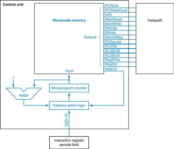
FIGURE D.4.6 The control unit as a microcode.
The use of the word “micro” serves to distinguish between the program counter in the datapath and the microprogram counter, and between the microcode memory and the instruction memory.
D.5 Translating a Microprogram to Hardware
To translate a microprogram into actual hardware, we need to specify how each field translates into control signals. We can implement a microprogram with either finite-state control or a microcode implementation with an explicit sequencer. If we choose a finite-state machine, we need to construct the nextstate function from the microprogram. Once this function is known, we can map a set of truth table entries for the nextstate outputs. In this section, we will show how to translate the microprogram, assuming that the next state is specified by a sequencer. From the truth tables we will construct, it would be straightforward to build the nextstate function for a finite-state machine.
Assuming an explicit sequencer, we need to do two additional tasks to translate the microprogram: assign addresses to the microinstructions and fill in the contents of the dispatch ROMs. This process is essentially the same as the process of translating an assembly language program into machine instructions: the fields of the assembly language or microprogram instruction are translated, and labels on the instructions must be resolved to addresses.
Figure D.5.1 shows the various values for each microinstruction field that controls the datapath and how these fields are encoded as control signals. If the field corresponding to a signal that affects a unit with state (i.e., Memory, Memory register, ALU destination, or PCWriteControl) is blank, then no control signal should be active. If a field corresponding to a multiplexor control signal or the ALU operation control (i.e., ALUOp, SRC1, or SRC2) is blank, the output is unused, so the associated signals may be set as don’t care.
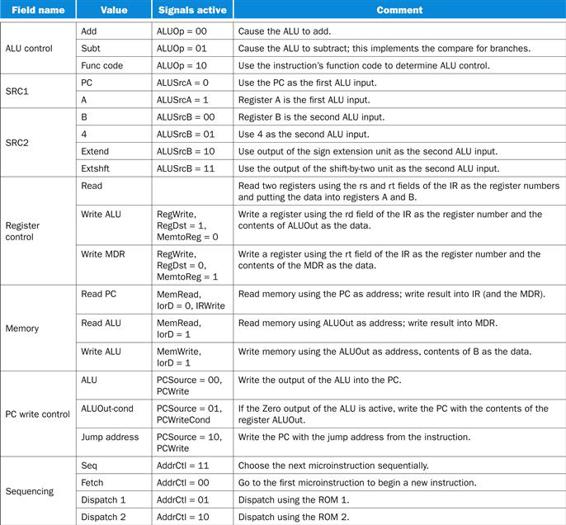
FIGURE D.5.1 Each microcode field translates to a set of control signals to be set.
These 22 different values of the fields specify all the required combinations of the 18 control lines. Control lines that are not set, which correspond to actions, are 0 by default. Multiplexor control lines are set to 0 if the output matters. If a multiplexor control line is not explicitly set, its output is a don’t care and is not used.
The sequencing field can have four values: Fetch (meaning go to the Fetch state), Dispatch 1, Dispatch 2, and Seq. These four values are encoded to set the 2-bit address control just as they were in Figure D.4.4: Fetch = 0, Dispatch 1 = 1, Dispatch 2 = 2, Seq = 3. Finally, we need to specify the contents of the dispatch tables to relate the dispatch entries of the sequence field to the symbolic labels in the microprogram. We use the same dispatch tables as we did earlier in Figure D.4.3.
A microcode assembler would use the encoding of the sequencing field, the contents of the symbolic dispatch tables in Figure D.5.2, the specification in Figure D.5.1, and the actual microprogram to generate the microinstructions.
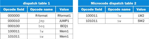
FIGURE D.5.2 The two microcode dispatch ROMs showing the contents in symbolic form and using the labels in the microprogram.
Since the microprogram is an abstract representation of the control, there is a great deal of flexibility in how the microprogram is translated. For example, the address assigned to many of the microinstructions can be chosen arbitrarily; the only restrictions are those imposed by the fact that certain microinstructions must occur in sequential order (so that incrementing the State register generates the address of the next instruction). Thus the microcode assembler may reduce the complexity of the control by assigning the microinstructions cleverly.
Organizing the Control to Reduce the Logic
For a machine with complex control, there may be a great deal of logic in the control unit. The control ROM or PLA may be very costly. Although our simple implementation had only an 18-bit microinstruction (assuming an explicit sequencer), there have been machines with microinstructions that are hundreds of bits wide. Clearly, a designer would like to reduce the number of microinstructions and the width.
The ideal approach to reducing control store is to first write the complete microprogram in a symbolic notation and then measure how control lines are set in each microinstruction. By taking measurements we are able to recognize control bits that can be encoded into a smaller field. For example, if no more than one of eight lines is set simultaneously in the same microinstruction, then this subset of control lines can be encoded into a 3-bit field (log2 8 55 3). This change saves five bits in every microinstruction and does not hurt CPI, though it does mean the extra hardware cost of a 3-to-8 decoder needed to generate the eight control lines when they are required at the datapath. It may also have some small clock cycle impact, since the decoder is in the signal path. However, shaving five bits off control store width will usually overcome the cost of the decoder, and the cycle time impact will probably be small or nonexistent. For example, this technique can be applied to bits 13–6 of the microinstructions in this machine, since only one of the seven bits of the control word is ever active (see Figure D.4.5).
This technique of reducing field width is called encoding. To further save space, control lines may be encoded together if they are only occasionally set in the same microinstruction; two microinstructions instead of one are then required when both must be set. As long as this doesn’t happen in critical routines, the narrower microinstruction may justify a few extra words of control store.
Microinstructions can be made narrower still if they are broken into different formats and given an opcode or format field to distinguish them. The format field gives all the unspecified control lines their default values, so as not to change anything else in the machine, and is similar to the opcode of an instruction in a more powerful instruction set. For example, we could use a different format for microinstructions that did memory accesses from those that did register-register ALU operations, taking advantage of the fact that the memory access control lines are not needed in microinstructions controlling ALU operations.
Reducing hardware costs by using format fields usually has an additional performance cost beyond the requirement for more decoders. A microprogram using a single microinstruction format can specify any combination of operations in a datapath and can take fewer clock cycles than a microprogram made up of restricted microinstructions that cannot perform any combination of operations in a single microinstruction. However, if the full capability of the wider microprogram word is not heavily used, then much of the control store will be wasted, and the machine could be made smaller and faster by restricting the microinstruction capability.
The narrow, but usually longer, approach is often called vertical microcode, while the wide but short approach is called horizontal microcode. It should be noted that the terms “vertical microcode” and “horizontal microcode” have no universal definition—the designers of the 8086 considered its 21-bit microinstruction to be more horizontal than other single-chip computers of the time. The related terms maximally encodedand minimally encoded are probably better than vertical and horizontal.
D.6 Concluding Remarks
We began this appendix by looking at how to translate a finite-state diagram to an implementation using a finite-state machine. We then looked at explicit sequencers that use a different technique for realizing the nextstate function. Although large microprograms are often targeted at implementations using this explicit nextstate approach, we can also implement a microprogram with a finite-state machine. As we saw, both ROM and PLA implementations of the logic functions are possible. The advantages of explicit versus encoded next state and ROM versus PLA implementation are summarized below.
The BIG Picture
Independent of whether the control is represented as a finite-state diagram or as a microprogram, translation to a hardware control implementation is similar. Each state or microinstruction asserts a set of control outputs and specifies how to choose the next state.
The nextstate function may be implemented by either encoding it in a finite-state machine or using an explicit sequencer. The explicit sequencer is more efficient if the number of states is large and there are many sequences of consecutive states without branching.
The control logic may be implemented with either ROMs or PLAs (or even a mix). PLAs are more efficient unless the control function is very dense. ROMs may be appropriate if the control is stored in a separate memory, as opposed to within the same chip as the datapath.
D.7 Exercises
D.1 [10] <§D.2> Instead of using four state bits to implement the finite-state machine in Figure D.3.1 on page C-9, use nine state bits, each of which is a 1 only if the finite-state machine is in that particular state (e.g., S1 is 1 in state 1, S2 is 1 in state 2, etc.). Redraw the PLA (Figure D.3.9).
D.2 [5] <§D.3> We wish to add the instruction jal (jump and link). Make any necessary changes to the datapath or to the control signals if needed. You can photocopy figures to make it faster to show the additions. How many product terms are required in a PLA that implements the control for the single-cycle datapath for jal?
D.3 [5] <§D.3> Now we wish to add the instruction addi (add immediate). Add any necessary changes to the datapath and to the control signals. How many product terms are required in a PLA that implements the control for the single-cycle datapath for addiu?
D.4 [10] <§D.3> Determine the number of product terms in a PLA that implements the finite-state machine for addi. The easiest way to do this is to construct the additions to the truth tables for addi.
D.5 [20] <§D.4> Implement the finite-state machine of using an explicit counter to determine the next state. Fill in the new entries for the additions to Figure D.4.5. Also, add any entries needed to the dispatch ROMs of Figure D.5.2.
D.6 [15] <§§D.3–D.6> Determine the size of the PLAs needed to implement the multicycle machine, assuming that the nextstate function is implemented with a counter. Implement the dispatch tables of Figure D.5.2 using two PLAs and the contents of the main control unit in Figure D.4.5 using another PLA. How does the total size of this solution compare to the single PLA solution with the next state encoded? What if the main PLAs for both approaches are split into two separate PLAs by factoring out the nextstate or address select signals?
All materials on the site are licensed Creative Commons Attribution-Sharealike 3.0 Unported CC BY-SA 3.0 & GNU Free Documentation License (GFDL)
If you are the copyright holder of any material contained on our site and intend to remove it, please contact our site administrator for approval.
© 2016-2026 All site design rights belong to S.Y.A.