Computer Organization and Design (2016)
The Processor
This chapter describes how processors exploit implicit parallelism. It contains an explanation of the principles and techniques used in implementing a processor, starting with a highly abstract and simplified overview. The overview is followed by a section that builds up a datapath and constructs a simple version of a processor sufficient to implement an instruction set like MIPS. The bulk of the chapter covers a more realistic pipelined MIPS implementation, and concludes with a section that develops the concepts necessary to implement more complex instruction sets, like the x86.
Keywords
ARM Cortex-A8; Intel Core i7; logic design; datapath; pipelining; control hazard; instruction-level parallelism; digital design; combinational element; state element; asserted; deasserted; clocking methodology; edge-triggered clocking; control signal; data signal; datapath element; program counter; PC; register file; sign-extend; branch target address; branch taken; branch not taken; untaken branch; delayed branch; truth table; don’t-care term; opcode; single-cycle implementation; pipelining; structural hazard; data hazard; forwarding; bypassing; load-use data hazard; pipeline stall; bubble; control hazard; branch hazard; branch prediction; latency; nop; flush; dynamic branch prediction; branch prediction buffer; branch history table; branch delay slot; branch target buffer; correlating predictor; tournament branch predictor; exception; interrupt; vectored interrupt; imprecise interrupt; imprecise exception; precise interrupt; precise exception; parallelism; instruction-level parallelism; multiple issue; static multiple issue; dynamic multiple issue; issue slots; speculation; issue packet; Very Long Instruction Word; VLIW; use latency; loop unrolling; register renaming; antidependence; name dependence; superscalar; dynamic pipeline scheduling; commit unit; reservation station; reorder buffer; out-of-order execution; in-order commit; microarchitecture; architectural registers; instruction latency; matrix multiply; ARM Cortex-A8; Intel Core i7
In a major matter, no details are small.
French Proverb
4.1 Introduction
4.2 Logic Design Conventions
4.3 Building a Datapath
4.4 A Simple Implementation Scheme
4.5 An Overview of Pipelining
4.6 Pipelined Datapath and Control
4.7 Data Hazards: Forwarding versus Stalling
4.8 Control Hazards
4.9 Exceptions
4.10 Parallelism via Instructions
4.11 Real Stuff: The ARM Cortex-A8 and Intel Core i7 Pipelines
4.12 Going Faster: Instruction-Level Parallelism and Matrix Multiply
![]() 4.13 Advanced Topic: an Introduction to Digital Design Using a Hardware Design Language to Describe and Model a Pipeline and More Pipelining Illustrations
4.13 Advanced Topic: an Introduction to Digital Design Using a Hardware Design Language to Describe and Model a Pipeline and More Pipelining Illustrations
4.14 Fallacies and Pitfalls
4.15 Concluding Remarks
![]() 4.16 Historical Perspective and Further Reading
4.16 Historical Perspective and Further Reading
4.17 Exercises
The Five Classic Components of a Computer
4.1 Introduction
Chapter 1 explains that the performance of a computer is determined by three key factors: instruction count, clock cycle time, and clock cycles per instruction (CPI). Chapter 2 explains that the compiler and the instruction set architecture determine the instruction count required for a given program. However, the implementation of the processor determines both the clock cycle time and the number of clock cycles per instruction. In this chapter, we construct the datapath and control unit for two different implementations of the MIPS instruction set.
This chapter contains an explanation of the principles and techniques used in implementing a processor, starting with a highly abstract and simplified overview in this section. It is followed by a section that builds up a datapath and constructs a simple version of a processor sufficient to implement an instruction set like MIPS. The bulk of the chapter covers a more realistic pipelined MIPS implementation, followed by a section that develops the concepts necessary to implement more complex instruction sets, like the x86.

For the reader interested in understanding the high-level interpretation of instructions and its impact on program performance, this initial section and Section 4.5 present the basic concepts of pipelining. Recent trends are covered in Section 4.10, and Section 4.11 describes the recent Intel Core i7 and ARM Cortex-A8 architectures. Section 4.12 shows how to use instruction-level parallelism to more than double the performance of the matrix multiply from Section 3.8. These sections provide enough background to understand the pipeline concepts at a high level.
For the reader interested in understanding the processor and its performance in more depth, Sections 4.3, 4.4, and 4.6 will be useful. Those interested in learning how to build a processor should also cover 4.2, 4.7, 4.8, and 4.9. For readers with an interest in modern hardware design, ![]() Section 4.13 describes how hardware design languages and CAD tools are used to implement hardware, and then how to use a hardware design language to describe a pipelined implementation. It also gives several more illustrations of how pipelining hardware executes.
Section 4.13 describes how hardware design languages and CAD tools are used to implement hardware, and then how to use a hardware design language to describe a pipelined implementation. It also gives several more illustrations of how pipelining hardware executes.
A Basic MIPS Implementation
We will be examining an implementation that includes a subset of the core MIPS instruction set:
■ The memory-reference instructions load word (lw) and store word (sw)
■ The arithmetic-logical instructions add, sub, AND, OR, and slt
■ The instructions branch equal (beq) and jump (j), which we add last
This subset does not include all the integer instructions (for example, shift, multiply, and divide are missing), nor does it include any floating-point instructions. However, it illustrates the key principles used in creating a datapath and designing the control. The implementation of the remaining instructions is similar.
In examining the implementation, we will have the opportunity to see how the instruction set architecture determines many aspects of the implementation, and how the choice of various implementation strategies affects the clock rate and CPI for the computer. Many of the key design principles introduced in Chapter 1 can be illustrated by looking at the implementation, such as Simplicity favors regularity. In addition, most concepts used to implement the MIPS subset in this chapter are the same basic ideas that are used to construct a broad spectrum of computers, from high-performance servers to general-purpose microprocessors to embedded processors.
An Overview of the Implementation
In Chapter 2, we looked at the core MIPS instructions, including the integer arithmetic-logical instructions, the memory-reference instructions, and the branch instructions. Much of what needs to be done to implement these instructions is the same, independent of the exact class of instruction. For every instruction, the first two steps are identical:
1. Send the program counter (PC) to the memory that contains the code and fetch the instruction from that memory.
2. Read one or two registers, using fields of the instruction to select the registers to read. For the load word instruction, we need to read only one register, but most other instructions require that we read two registers.
After these two steps, the actions required to complete the instruction depend on the instruction class. Fortunately, for each of the three instruction classes (memory-reference, arithmetic-logical, and branches), the actions are largely the same, independent of the exact instruction. The simplicity and regularity of the MIPS instruction set simplifies the implementation by making the execution of many of the instruction classes similar.
For example, all instruction classes, except jump, use the arithmetic-logical unit (ALU) after reading the registers. The memory-reference instructions use the ALU for an address calculation, the arithmetic-logical instructions for the operation execution, and branches for comparison. After using the ALU, the actions required to complete various instruction classes differ. A memory-reference instruction will need to access the memory either to read data for a load or write data for a store. An arithmetic-logical or load instruction must write the data from the ALU or memory back into a register. Lastly, for a branch instruction, we may need to change the next instruction address based on the comparison; otherwise, the PC should be incremented by 4 to get the address of the next instruction.
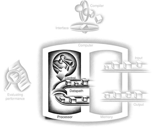
Figure 4.1 shows the high-level view of a MIPS implementation, focusing on the various functional units and their interconnection. Although this figure shows most of the flow of data through the processor, it omits two important aspects of instruction execution.
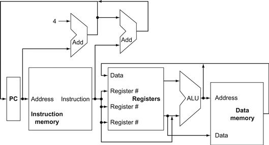
FIGURE 4.1 An abstract view of the implementation of the MIPS subset showing the major functional units and the major connections between them.
All instructions start by using the program counter to supply the instruction address to the instruction memory. After the instruction is fetched, the register operands used by an instruction are specified by fields of that instruction. Once the register operands have been fetched, they can be operated on to compute a memory address (for a load or store), to compute an arithmetic result (for an integer arithmetic-logical instruction), or a compare (for a branch). If the instruction is an arithmetic-logical instruction, the result from the ALU must be written to a register. If the operation is a load or store, the ALU result is used as an address to either store a value from the registers or load a value from memory into the registers. The result from the ALU or memory is written back into the register file. Branches require the use of the ALU output to determine the next instruction address, which comes either from the ALU (where the PC and branch offset are summed) or from an adder that increments the current PC by 4. The thick lines interconnecting the functional units represent buses, which consist of multiple signals. The arrows are used to guide the reader in knowing how information flows. Since signal lines may cross, we explicitly show when crossing lines are connected by the presence of a dot where the lines cross.
First, in several places, Figure 4.1 shows data going to a particular unit as coming from two different sources. For example, the value written into the PC can come from one of two adders, the data written into the register file can come from either the ALU or the data memory, and the second input to the ALU can come from a register or the immediate field of the instruction. In practice, these data lines cannot simply be wired together; we must add a logic element that chooses from among the multiple sources and steers one of those sources to its destination. This selection is commonly done with a device called a multiplexor, although this device might better be called a data selector. Appendix B describes the multiplexor, which selects from among several inputs based on the setting of its control lines. The control lines are set based primarily on information taken from the instruction being executed.
The second omission in Figure 4.1 is that several of the units must be controlled depending on the type of instruction. For example, the data memory must read on a load and write on a store. The register file must be written on a load an arithmetic-logical instruction. And, of course, the ALU must perform one of several operations. (![]() Appendix B describes the detailed design of the ALU.) Like the multiplexors, control lines that are set on the basis of various fields in the instruction direct these operations.
Appendix B describes the detailed design of the ALU.) Like the multiplexors, control lines that are set on the basis of various fields in the instruction direct these operations.
Figure 4.2 shows the datapath of Figure 4.1 with the three required multiplexors added, as well as control lines for the major functional units. A control unit, which has the instruction as an input, is used to determine how to set the control lines for the functional units and two of the multiplexors. The third multiplexor, which determines whether PC+4 or the branch destination address is written into the PC, is set based on the Zero output of the ALU, which is used to perform the comparison of a beq instruction. The regularity and simplicity of the MIPS instruction set means that a simple decoding process can be used to determine how to set the control lines.
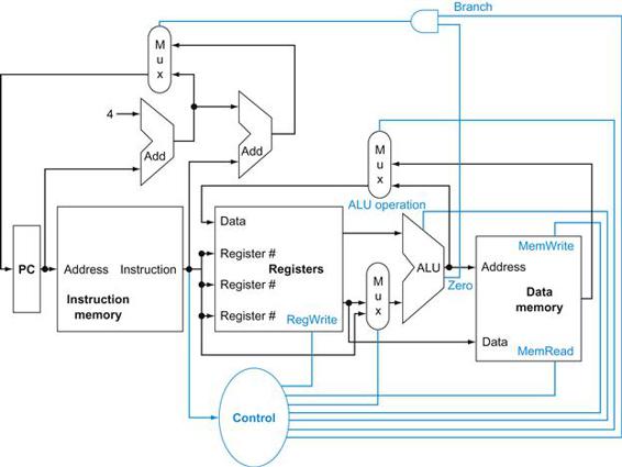
FIGURE 4.2 The basic implementation of the MIPS subset, including the necessary multiplexors and control lines.
The top multiplexor (“Mux”) controls what value replaces the PC (PC+4 or the branch destination address); the multiplexor is controlled by the gate that “ANDs” together the Zero output of the ALU and a control signal that indicates that the instruction is a branch. The middle multiplexor, whose output returns to the register file, is used to steer the output of the ALU (in the case of an arithmetic-logical instruction) or the output of the data memory (in the case of a load) for writing into the register file. Finally, the bottommost multiplexor is used to determine whether the second ALU input is from the registers (for an arithmetic-logical instruction or a branch) or from the offset field of the instruction (for a load or store). The added control lines are straightforward and determine the operation performed at the ALU, whether the data memory should read or write, and whether the registers should perform a write operation. The control lines are shown in color to make them easier to see.
In the remainder of the chapter, we refine this view to fill in the details, which requires that we add further functional units, increase the number of connections between units, and, of course, enhance a control unit to control what actions are taken for different instruction classes. Sections 4.3 and 4.4 describe a simple implementation that uses a single long clock cycle for every instruction and follows the general form of Figures 4.1 and 4.2. In this first design, every instruction begins execution on one clock edge and completes execution on the next clock edge.
While easier to understand, this approach is not practical, since the clock cycle must be severely stretched to accommodate the longest instruction. After designing the control for this simple computer, we will look at pipelined implementation with all its complexities, including exceptions.
Check Yourself
How many of the five classic components of a computer—shown on page 243—do Figures 4.1 and 4.2 include?
4.2 Logic Design Conventions
To discuss the design of a computer, we must decide how the hardware logic implementing the computer will operate and how the computer is clocked. This section reviews a few key ideas in digital logic that we will use extensively in this chapter. If you have little or no background in digital logic, you will find it helpful to read ![]() Appendix B before continuing.
Appendix B before continuing.
The datapath elements in the MIPS implementation consist of two different types of logic elements: elements that operate on data values and elements that contain state. The elements that operate on data values are all combinational, which means that their outputs depend only on the current inputs. Given the same input, a combinational element always produces the same output. The ALU shown in Figure 4.1and discussed in ![]() Appendix B is an example of a combinational element. Given a set of inputs, it always produces the same output because it has no internal storage.
Appendix B is an example of a combinational element. Given a set of inputs, it always produces the same output because it has no internal storage.
combinational element
An operational element, such as an AND gate or an ALU.
Other elements in the design are not combinational, but instead contain state. An element contains state if it has some internal storage. We call these elements state elements because, if we pulled the power plug on the computer, we could restart it accurately by loading the state elements with the values they contained before we pulled the plug. Furthermore, if we saved and restored the state elements, it would be as if the computer had never lost power. Thus, these state elements completely characterize the computer. In Figure 4.1, the instruction and data memories, as well as the registers, are all examples of state elements.
state element
A memory element, such as a register or a memory.
A state element has at least two inputs and one output. The required inputs are the data value to be written into the element and the clock, which determines when the data value is written. The output from a state element provides the value that was written in an earlier clock cycle. For example, one of the logically simplest state elements is a D-type flip-flop (see ![]() Appendix B), which has exactly these two inputs (a value and a clock) and one output. In addition to flip-flops, our MIPS implementation uses two other types of state elements: memories and registers, both of which appear in Figure 4.1. The clock is used to determine when the state element should be written; a state element can be read at any time.
Appendix B), which has exactly these two inputs (a value and a clock) and one output. In addition to flip-flops, our MIPS implementation uses two other types of state elements: memories and registers, both of which appear in Figure 4.1. The clock is used to determine when the state element should be written; a state element can be read at any time.
Logic components that contain state are also called sequential, because their outputs depend on both their inputs and the contents of the internal state. For example, the output from the functional unit representing the registers depends both on the register numbers supplied and on what was written into the registers previously. The operation of both the combinational and sequential elements and their construction are discussed in more detail in ![]() Appendix B.
Appendix B.
Clocking Methodology
A clocking methodology defines when signals can be read and when they can be written. It is important to specify the timing of reads and writes, because if a signal is written at the same time it is read, the value of the read could correspond to the old value, the newly written value, or even some mix of the two! Computer designs cannot tolerate such unpredictability. A clocking methodology is designed to make hardware predictable.
clocking methodology
The approach used to determine when data is valid and stable relative to the clock.
For simplicity, we will assume an edge-triggered clocking methodology. An edge-triggered clocking methodology means that any values stored in a sequential logic element are updated only on a clock edge, which is a quick transition from low to high or vice versa (see Figure 4.3). Because only state elements can store a data value, any collection of combinational logic must have its inputs come from a set of state elements and its outputs written into a set of state elements. The inputs are values that were written in a previous clock cycle, while the outputs are values that can be used in a following clock cycle.
edge-triggered clocking
A clocking scheme in which all state changes occur on a clock edge.
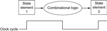
FIGURE 4.3 Combinational logic, state elements, and the clock are closely related.
In a synchronous digital system, the clock determines when elements with state will write values into internal storage. Any inputs to a state element must reach a stable value (that is, have reached a value from which they will not change until after the clock edge) before the active clock edge causes the state to be updated. All state elements in this chapter, including memory, are assumed to be positive edge-triggered; that is, they change on the rising clock edge.
Figure 4.3 shows the two state elements surrounding a block of combinational logic, which operates in a single clock cycle: all signals must propagate from state element 1, through the combinational logic, and to state element 2 in the time of one clock cycle. The time necessary for the signals to reach state element 2 defines the length of the clock cycle.
For simplicity, we do not show a write control signal when a state element is written on every active clock edge. In contrast, if a state element is not updated on every clock, then an explicit write control signal is required. Both the clock signal and the write control signal are inputs, and the state element is changed only when the write control signal is asserted and a clock edge occurs.
control signal
A signal used for multiplexor selection or for directing the operation of a functional unit; contrasts with a data signal, which contains information that is operated on by a functional unit.
We will use the word asserted to indicate a signal that is logically high and assert to specify that a signal should be driven logically high, and deassert or deasserted to represent logically low. We use the terms assert and deassert because when we implement hardware, at times 1 represents logically high and at times it can represent logically low.
asserted
The signal is logically high or true.
deasserted
The signal is logically low or false.
An edge-triggered methodology allows us to read the contents of a register, send the value through some combinational logic, and write that register in the same clock cycle. Figure 4.4 gives a generic example. It doesn’t matter whether we assume that all writes take place on the rising clock edge (from low to high) or on the falling clock edge (from high to low), since the inputs to the combinational logic block cannot change except on the chosen clock edge. In this book we use the rising clock edge. With an edge-triggered timing methodology, there is no feedback within a single clock cycle, and the logic in Figure 4.4 works correctly. In ![]() Appendix B, we briefly discuss additional timing constraints (such as setup and hold times) as well as other timing methodologies.
Appendix B, we briefly discuss additional timing constraints (such as setup and hold times) as well as other timing methodologies.
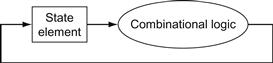
FIGURE 4.4 An edge-triggered methodology allows a state element to be read and written in the same clock cycle without creating a race that could lead to indeterminate data values.
Of course, the clock cycle still must be long enough so that the input values are stable when the active clock edge occurs. Feedback cannot occur within one clock cycle because of the edge-triggered update of the state element. If feedback were possible, this design could not work properly. Our designs in this chapter and the next rely on the edge-triggered timing methodology and on structures like the one shown in this figure.
For the 32-bit MIPS architecture, nearly all of these state and logic elements will have inputs and outputs that are 32 bits wide, since that is the width of most of the data handled by the processor. We will make it clear whenever a unit has an input or output that is other than 32 bits in width. The figures will indicate buses, which are signals wider than 1 bit, with thicker lines. At times, we will want to combine several buses to form a wider bus; for example, we may want to obtain a 32-bit bus by combining two 16-bit buses. In such cases, labels on the bus lines will make it clear that we are concatenating buses to form a wider bus. Arrows are also added to help clarify the direction of the flow of data between elements. Finally, color indicates a control signal as opposed to a signal that carries data; this distinction will become clearer as we proceed through this chapter.
Check Yourself
True or false: Because the register file is both read and written on the same clock cycle, any MIPS datapath using edge-triggered writes must have more than one copy of the register file.
Elaboration
There is also a 64-bit version of the MIPS architecture, and, naturally enough, most paths in its implementation would be 64 bits wide.
4.3 Building a Datapath
A reasonable way to start a datapath design is to examine the major components required to execute each class of MIPS instructions. Let’s start at the top by looking at which datapath elements each instruction needs, and then work our way down through the levels of abstraction. When we show the datapath elements, we will also show their control signals. We use abstraction in this explanation, starting from the bottom up.

datapath element
A unit used to operate on or hold data within a processor. In the MIPS implementation, the datapath elements include the instruction and data memories, the register file, the ALU, and adders.
Figure 4.5a shows the first element we need: a memory unit to store the instructions of a program and supply instructions given an address. Figure 4.5b also shows the program counter (PC), which as we saw in Chapter 2 is a register that holds the address of the current instruction. Lastly, we will need an adder to increment the PC to the address of the next instruction. This adder, which is combinational, can be built from the ALU described in detail in ![]() Appendix B simply by wiring the control lines so that the control always specifies an add operation. We will draw such an ALU with the label Add, as in Figure 4.5, to indicate that it has been permanently made an adder and cannot perform the other ALU functions.
Appendix B simply by wiring the control lines so that the control always specifies an add operation. We will draw such an ALU with the label Add, as in Figure 4.5, to indicate that it has been permanently made an adder and cannot perform the other ALU functions.
program counter (PC)
The register containing the address of the instruction in the program being executed.
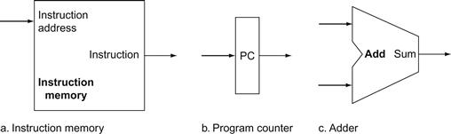
FIGURE 4.5 Two state elements are needed to store and access instructions, and an adder is needed to compute the next instruction address.
The state elements are the instruction memory and the program counter. The instruction memory need only provide read access because the datapath does not write instructions. Since the instruction memory only reads, we treat it as combinational logic: the output at any time reflects the contents of the location specified by the address input, and no read control signal is needed. (We will need to write the instruction memory when we load the program; this is not hard to add, and we ignore it for simplicity.) The program counter is a 32-bit register that is written at the end of every clock cycle and thus does not need a write control signal. The adder is an ALU wired to always add its two 32-bit inputs and place the sum on its output.
To execute any instruction, we must start by fetching the instruction from memory. To prepare for executing the next instruction, we must also increment the program counter so that it points at the next instruction, 4 bytes later. Figure 4.6 shows how to combine the three elements from Figure 4.5 to form a datapath that fetches instructions and increments the PC to obtain the address of the next sequential instruction.
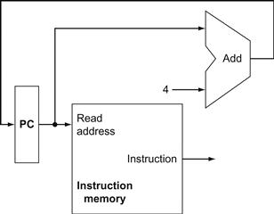
FIGURE 4.6 A portion of the datapath used for fetching instructions and incrementing the program counter.
The fetched instruction is used by other parts of the datapath.
Now let’s consider the R-format instructions (see Figure 2.20 on page 120). They all read two registers, perform an ALU operation on the contents of the registers, and write the result to a register. We call these instructions either R-type instructions or arithmetic-logical instructions (since they perform arithmetic or logical operations). This instruction class includes add, sub, AND, OR, and slt, which were introduced in Chapter 2. Recall that a typical instance of such an instruction is add $t1,$t2,$t3, which reads $t2 and $t3 and writes $t1.
The processor’s 32 general-purpose registers are stored in a structure called a register file. A register file is a collection of registers in which any register can be read or written by specifying the number of the register in the file. The register file contains the register state of the computer. In addition, we will need an ALU to operate on the values read from the registers.
register file
A state element that consists of a set of registers that can be read and written by supplying a register number to be accessed.
R-format instructions have three register operands, so we will need to read two data words from the register file and write one data word into the register file for each instruction. For each data word to be read from the registers, we need an input to the register file that specifies the register number to be read and an output from the register file that will carry the value that has been read from the registers. To write a data word, we will need two inputs: one to specify the register number to be written and one to supply the data to be written into the register. The register file always outputs the contents of whatever register numbers are on the Read register inputs. Writes, however, are controlled by the write control signal, which must be asserted for a write to occur at the clock edge. Figure 4.7a shows the result; we need a total of four inputs (three for register numbers and one for data) and two outputs (both for data). The register number inputs are 5 bits wide to specify one of 32 registers (32=25), whereas the data input and two data output buses are each 32 bits wide.
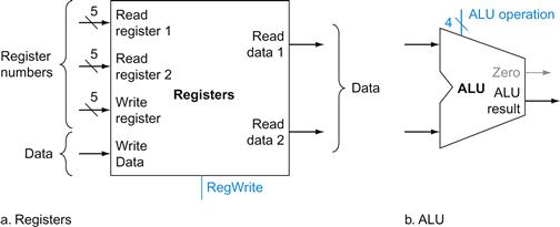
FIGURE 4.7 The two elements needed to implement R-format ALU operations are the register file and the ALU.
The register file contains all the registers and has two read ports and one write port. The design of multiported register files is discussed in Section B.8 of ![]() Appendix B. The register file always outputs the contents of the registers corresponding to the Read register inputs on the outputs; no other control inputs are needed. In contrast, a register write must be explicitly indicated by asserting the write control signal. Remember that writes are edge-triggered, so that all the write inputs (i.e., the value to be written, the register number, and the write control signal) must be valid at the clock edge. Since writes to the register file are edge-triggered, our design can legally read and write the same register within a clock cycle: the read will get the value written in an earlier clock cycle, while the value written will be available to a read in a subsequent clock cycle. The inputs carrying the register number to the register file are all 5 bits wide, whereas the lines carrying data values are 32 bits wide. The operation to be performed by the ALU is controlled with the ALU operation signal, which will be 4 bits wide, using the ALU designed in
Appendix B. The register file always outputs the contents of the registers corresponding to the Read register inputs on the outputs; no other control inputs are needed. In contrast, a register write must be explicitly indicated by asserting the write control signal. Remember that writes are edge-triggered, so that all the write inputs (i.e., the value to be written, the register number, and the write control signal) must be valid at the clock edge. Since writes to the register file are edge-triggered, our design can legally read and write the same register within a clock cycle: the read will get the value written in an earlier clock cycle, while the value written will be available to a read in a subsequent clock cycle. The inputs carrying the register number to the register file are all 5 bits wide, whereas the lines carrying data values are 32 bits wide. The operation to be performed by the ALU is controlled with the ALU operation signal, which will be 4 bits wide, using the ALU designed in ![]() Appendix B. We will use the Zero detection output of the ALU shortly to implement branches. The overflow output will not be needed until Section 4.9, when we discuss exceptions; we omit it until then.
Appendix B. We will use the Zero detection output of the ALU shortly to implement branches. The overflow output will not be needed until Section 4.9, when we discuss exceptions; we omit it until then.
Figure 4.7b shows the ALU, which takes two 32-bit inputs and produces a 32-bit result, as well as a 1-bit signal if the result is 0. The 4-bit control signal of the ALU is described in detail in ![]() Appendix B; we will review the ALU control shortly when we need to know how to set it.
Appendix B; we will review the ALU control shortly when we need to know how to set it.
Next, consider the MIPS load word and store word instructions, which have the general form lw $t1,offset_value($t2) or sw $t1,offset_value ($t2). These instructions compute a memory address by adding the base register, which is $t2, to the 16-bit signed offset field contained in the instruction. If the instruction is a store, the value to be stored must also be read from the register file where it resides in $t1. If the instruction is a load, the value read from memory must be written into the register file in the specified register, which is $t1. Thus, we will need both the register file and the ALU from Figure 4.7.
In addition, we will need a unit to sign-extend the 16-bit offset field in the instruction to a 32-bit signed value, and a data memory unit to read from or write to. The data memory must be written on store instructions; hence, data memory has read and write control signals, an address input, and an input for the data to be written into memory. Figure 4.8 shows these two elements.
sign-extend
To increase the size of a data item by replicating the high-order sign bit of the original data item in the high-order bits of the larger, destination data item.
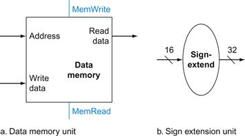
FIGURE 4.8 The two units needed to implement loads and stores, in addition to the register file and ALU of Figure 4.7, are the data memory unit and the sign extension unit.
The memory unit is a state element with inputs for the address and the write data, and a single output for the read result. There are separate read and write controls, although only one of these may be asserted on any given clock. The memory unit needs a read signal, since, unlike the register file, reading the value of an invalid address can cause problems, as we will see in Chapter 5. The sign extension unit has a 16-bit input that is sign-extended into a 32-bit result appearing on the output (see Chapter 2). We assume the data memory is edge-triggered for writes. Standard memory chips actually have a write enable signal that is used for writes. Although the write enable is not edge-triggered, our edge-triggered design could easily be adapted to work with real memory chips. See Section B.8 of ![]() Appendix B for further discussion of how real memory chips work.
Appendix B for further discussion of how real memory chips work.
The beq instruction has three operands, two registers that are compared for equality, and a 16-bit offset used to compute the branch target address relative to the branch instruction address. Its form is beq $t1,$t2,offset. To implement this instruction, we must compute the branch target address by adding the sign-extended offset field of the instruction to the PC. There are two details in the definition of branch instructions (see Chapter 2) to which we must pay attention:
■ The instruction set architecture specifies that the base for the branch address calculation is the address of the instruction following the branch. Since we compute PC+4 (the address of the next instruction) in the instruction fetch datapath, it is easy to use this value as the base for computing the branch target address.
■ The architecture also states that the offset field is shifted left 2 bits so that it is a word offset; this shift increases the effective range of the offset field by a factor of 4.
branch target address
The address specified in a branch, which becomes the new program counter (PC) if the branch is taken. In the MIPS architecture the branch target is given by the sum of the offset field of the instruction and the address of the instruction following the branch.
To deal with the latter complication, we will need to shift the offset field by 2.
As well as computing the branch target address, we must also determine whether the next instruction is the instruction that follows sequentially or the instruction at the branch target address. When the condition is true (i.e., the operands are equal), the branch target address becomes the new PC, and we say that the branch is taken. If the operands are not equal, the incremented PC should replace the current PC (just as for any other normal instruction); in this case, we say that the branch is not taken.
branch taken
A branch where the branch condition is satisfied and the program counter (PC) becomes the branch target. All unconditional branches are taken branches.
branch not taken or (untaken branch)
A branch where the branch condition is false and the program counter (PC) becomes the address of the instruction that sequentially follows the branch.
Thus, the branch datapath must do two operations: compute the branch target address and compare the register contents. (Branches also affect the instruction fetch portion of the datapath, as we will deal with shortly.) Figure 4.9 shows the structure of the datapath segment that handles branches. To compute the branch target address, the branch datapath includes a sign extension unit, from Figure 4.8 and an adder. To perform the compare, we need to use the register file shown in Figure 4.7a to supply the two register operands (although we will not need to write into the register file). In addition, the comparison can be done using the ALU we designed in ![]() Appendix B. Since that ALU provides an output signal that indicates whether the result was 0, we can send the two register operands to the ALU with the control set to do a subtract. If the Zero signal out of the ALU unit is asserted, we know that the two values are equal. Although the Zero output always signals if the result is 0, we will be using it only to implement the equal test of branches. Later, we will show exactly how to connect the control signals of the ALU for use in the datapath.
Appendix B. Since that ALU provides an output signal that indicates whether the result was 0, we can send the two register operands to the ALU with the control set to do a subtract. If the Zero signal out of the ALU unit is asserted, we know that the two values are equal. Although the Zero output always signals if the result is 0, we will be using it only to implement the equal test of branches. Later, we will show exactly how to connect the control signals of the ALU for use in the datapath.
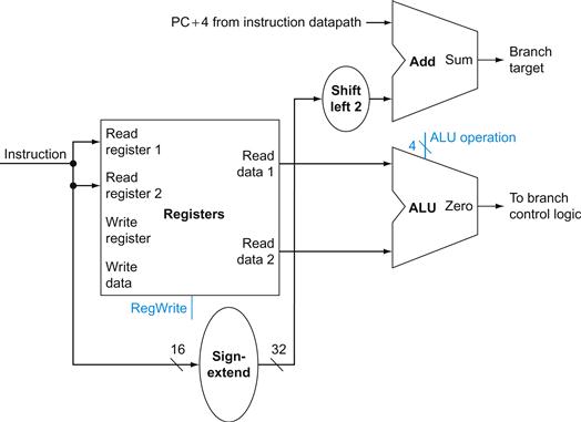
FIGURE 4.9 The datapath for a branch uses the ALU to evaluate the branch condition and a separate adder to compute the branch target as the sum of the incremented PC and the sign-extended, lower 16 bits of the instruction (the branch displacement), shifted left 2 bits.
The unit labeled Shift left 2 is simply a routing of the signals between input and output that adds 00two to the low-order end of the sign-extended offset field; no actual shift hardware is needed, since the amount of the “shift” is constant. Since we know that the offset was sign-extended from 16 bits, the shift will throw away only “sign bits.” Control logic is used to decide whether the incremented PC or branch target should replace the PC, based on the Zero output of the ALU.
The jump instruction operates by replacing the lower 28 bits of the PC with the lower 26 bits of the instruction shifted left by 2 bits. Simply concatenating 00 to the jump offset accomplishes this shift, as described in Chapter 2.
Elaboration
In the MIPS instruction set, branches are delayed, meaning that the instruction immediately following the branch is always executed, independent of whether the branch condition is true or false. When the condition is false, the execution looks like a normal branch. When the condition is true, a delayed branch first executes the instruction immediately following the branch in sequential instruction order before jumping to the specified branch target address. The motivation for delayed branches arises from how pipelining affects branches (see Section 4.8). For simplicity, we generally ignore delayed branches in this chapter and implement a nondelayed beq instruction.
delayed branch
A type of branch where the instruction immediately following the branch is always executed, independent of whether the branch condition is true or false.
Creating a Single Datapath
Now that we have examined the datapath components needed for the individual instruction classes, we can combine them into a single datapath and add the control to complete the implementation. This simplest datapath will attempt to execute all instructions in one clock cycle. This means that no datapath resource can be used more than once per instruction, so any element needed more than once must be duplicated. We therefore need a memory for instructions separate from one for data. Although some of the functional units will need to be duplicated, many of the elements can be shared by different instruction flows.
To share a datapath element between two different instruction classes, we may need to allow multiple connections to the input of an element, using a multiplexor and control signal to select among the multiple inputs.
Building a Datapath
Example
The operations of arithmetic-logical (or R-type) instructions and the memory instructions datapath are quite similar. The key differences are the following:
■ The arithmetic-logical instructions use the ALU, with the inputs coming from the two registers. The memory instructions can also use the ALU to do the address calculation, although the second input is the sign-extended 16-bit offset field from the instruction.
■ The value stored into a destination register comes from the ALU (for an R-type instruction) or the memory (for a load).
Show how to build a datapath for the operational portion of the memory-reference and arithmetic-logical instructions that uses a single register file and a single ALU to handle both types of instructions, adding any necessary multiplexors.
Answer
To create a datapath with only a single register file and a single ALU, we must support two different sources for the second ALU input, as well as two different sources for the data stored into the register file. Thus, one multiplexor is placed at the ALU input and another at the data input to the register file. Figure 4.10 shows the operational portion of the combined datapath.
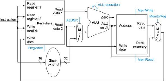
FIGURE 4.10 The datapath for the memory instructions and the R-type instructions.
This example shows how a single datapath can be assembled from the pieces in Figures 4.7 and 4.8 by adding multiplexors. Two multiplexors are needed, as described in the example.
Now we can combine all the pieces to make a simple datapath for the core MIPS architecture by adding the datapath for instruction fetch (Figure 4.6), the datapath from R-type and memory instructions (Figure 4.10), and the datapath for branches (Figure 4.9). Figure 4.11 shows the datapath we obtain by composing the separate pieces. The branch instruction uses the main ALU for comparison of the register operands, so we must keep the adder from Figure 4.9 for computing the branch target address. An additional multiplexor is required to select either the sequentially following instruction address (PC+4) or the branch target address to be written into the PC.
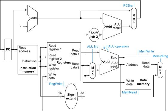
FIGURE 4.11 The simple datapath for the MIPS architecture combines the elements required by different instruction classes.
The components come from Figures 4.6, 4.9, and 4.10. This datapath can execute the basic instructions (load-store word, ALU operations, and branches) in a single clock cycle. An additional multiplexor is needed to integrate branches. The support for jumps will be added later.
Now that we have completed this simple datapath, we can add the control unit. The control unit must be able to take inputs and generate a write signal for each state element, the selector control for each multiplexor, and the ALU control. The ALU control is different in a number of ways, and it will be useful to design it first before we design the rest of the control unit.
Check Yourself
I. Which of the following is correct for a load instruction? Refer to Figure 4.10.
a. MemtoReg should be set to cause the data from memory to be sent to the register file.
b. MemtoReg should be set to cause the correct register destination to be sent to the register file.
c. We do not care about the setting of MemtoReg for loads.
II. The single-cycle datapath conceptually described in this section must have separate instruction and data memories, because
a. the formats of data and instructions are different in MIPS, and hence different memories are needed.
b. having separate memories is less expensive.
c. the processor operates in one cycle and cannot use a single-ported memory for two different accesses within that cycle
4.4 A Simple Implementation Scheme
In this section, we look at what might be thought of as the simplest possible implementation of our MIPS subset. We build this simple implementation using the datapath of the last section and adding a simple control function. This simple implementation covers load word (lw), store word (sw), branch equal (beq), and the arithmetic-logical instructions add, sub, AND, OR, and set on less than. We will later enhance the design to include a jump instruction (j).
The ALU Control
The MIPS ALU in ![]() Appendix B defines the 6 following combinations of four control inputs:
Appendix B defines the 6 following combinations of four control inputs:
|
ALU control lines |
Function |
|
0000 |
AND |
|
0001 |
OR |
|
0010 |
add |
|
0110 |
subtract |
|
0111 |
set on less than |
|
1100 |
NOR |
Depending on the instruction class, the ALU will need to perform one of these first five functions. (NOR is needed for other parts of the MIPS instruction set not found in the subset we are implementing.) For load word and store word instructions, we use the ALU to compute the memory address by addition. For the R-type instructions, the ALU needs to perform one of the five actions (AND, OR, subtract, add, or set on less than), depending on the value of the 6-bit funct (or function) field in the low-order bits of the instruction (see Chapter 2). For branch equal, the ALU must perform a subtraction.
We can generate the 4-bit ALU control input using a small control unit that has as inputs the function field of the instruction and a 2-bit control field, which we call ALUOp. ALUOp indicates whether the operation to be performed should be add (00) for loads and stores, subtract (01) for beq, or determined by the operation encoded in the funct field (10). The output of the ALU control unit is a 4-bit signal that directly controls the ALU by generating one of the 4-bit combinations shown previously.
In Figure 4.12, we show how to set the ALU control inputs based on the 2-bit ALUOp control and the 6-bit function code. Later in this chapter we will see how the ALUOp bits are generated from the main control unit.
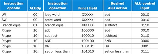
FIGURE 4.12 How the ALU control bits are set depends on the ALUOp control bits and the different function codes for the R-type instruction.
The opcode, listed in the first column, determines the setting of the ALUOp bits. All the encodings are shown in binary. Notice that when the ALUOp code is 00 or 01, the desired ALU action does not depend on the function code field; in this case, we say that we “don’t care” about the value of the function code, and the funct field is shown as XXXXXX. When the ALUOp value is 10, then the function code is used to set the ALU control input. See ![]() Appendix B.
Appendix B.
This style of using multiple levels of decoding—that is, the main control unit generates the ALUOp bits, which then are used as input to the ALU control that generates the actual signals to control the ALU unit—is a common implementation technique. Using multiple levels of control can reduce the size of the main control unit. Using several smaller control units may also potentially increase the speed of the control unit. Such optimizations are important, since the speed of the control unit is often critical to clock cycle time.
There are several different ways to implement the mapping from the 2-bit ALUOp field and the 6-bit funct field to the four ALU operation control bits. Because only a small number of the 64 possible values of the function field are of interest and the function field is used only when the ALUOp bits equal 10, we can use a small piece of logic that recognizes the subset of possible values and causes the correct setting of the ALU control bits.
As a step in designing this logic, it is useful to create a truth table for the interesting combinations of the function code field and the ALUOp bits, as we’ve done in Figure 4.13; this truth table shows how the 4-bit ALU control is set depending on these two input fields. Since the full truth table is very large (28=256 entries) and we don’t care about the value of the ALU control for many of these input combinations, we show only the truth table entries for which the ALU control must have a specific value. Throughout this chapter, we will use this practice of showing only the truth table entries for outputs that must be asserted and not showing those that are all deasserted or don’t care. (This practice has a disadvantage, which we discuss in Section D.2 of ![]() Appendix D.)
Appendix D.)
truth table
From logic, a representation of a logical operation by listing all the values of the inputs and then in each case showing what the resulting outputs should be.
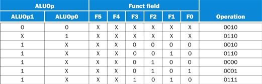
FIGURE 4.13 The truth table for the 4 ALU control bits (called Operation).
The inputs are the ALUOp and function code field. Only the entries for which the ALU control is asserted are shown. Some don’t-care entries have been added. For example, the ALUOp does not use the encoding 11, so the truth table can contain entries 1X and X1, rather than 10 and 01. Note that when the function field is used, the first 2 bits (F5 and F4) of these instructions are always 10, so they are don’t-care terms and are replaced with XX in the truth table.
Because in many instances we do not care about the values of some of the inputs, and because we wish to keep the tables compact, we also include don’t-care terms. A don’t-care term in this truth table (represented by an X in an input column) indicates that the output does not depend on the value of the input corresponding to that column. For example, when the ALUOp bits are 00, as in the first row of Figure 4.13, we always set the ALU control to 0010, independent of the function code. In this case, then, the function code inputs will be don’t cares in this line of the truth table. Later, we will see examples of another type of don’t-care term. If you are unfamiliar with the concept of don’t-care terms, see ![]() Appendix B for more information.
Appendix B for more information.
don’t-care term
An element of a logical function in which the output does not depend on the values of all the inputs. Don’t-care terms may be specified in different ways.
Once the truth table has been constructed, it can be optimized and then turned into gates. This process is completely mechanical. Thus, rather than show the final steps here, we describe the process and the result in Section D.2 of ![]() Appendix D.
Appendix D.
Designing the Main Control Unit
Now that we have described how to design an ALU that uses the function code and a 2-bit signal as its control inputs, we can return to looking at the rest of the control. To start this process, let’s identify the fields of an instruction and the control lines that are needed for the datapath we constructed in Figure 4.11. To understand how to connect the fields of an instruction to the datapath, it is useful to review the formats of the three instruction classes: the R-type, branch, and load-store instructions. Figure 4.14 shows these formats.
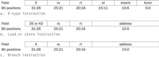
FIGURE 4.14 The three instruction classes (R-type, load and store, and branch) use two different instruction formats.
The jump instructions use another format, which we will discuss shortly. (a) Instruction format for R-format instructions, which all have an opcode of 0. These instructions have three register operands: rs, rt, and rd. Fields rs and rt are sources, and rd is the destination. The ALU function is in the funct field and is decoded by the ALU control design in the previous section. The R-type instructions that we implement are add, sub, AND, OR, and slt. The shamt field is used only for shifts; we will ignore it in this chapter. (b) Instruction format for load (opcode=35ten) and store (opcode=43ten) instructions. The register rs is the base register that is added to the 16-bit address field to form the memory address. For loads, rt is the destination register for the loaded value. For stores, rt is the source register whose value should be stored into memory. (c) Instruction format for branch equal (opcode=4). The registers rs and rt are the source registers that are compared for equality. The 16-bit address field is sign-extended, shifted, and added to the PC+4 to compute the branch target address.
There are several major observations about this instruction format that we will rely on:
■ The op field, which as we saw in Chapter 2 is called the opcode, is always contained in bits 31:26. We will refer to this field as Op[5:0].
■ The two registers to be read are always specified by the rs and rt fields, at positions 25:21 and 20:16. This is true for the R-type instructions, branch equal, and store.
■ The base register for load and store instructions is always in bit positions 25:21 (rs).
■ The 16-bit offset for branch equal, load, and store is always in positions 15:0.
■ The destination register is in one of two places. For a load it is in bit positions 20:16 (rt), while for an R-type instruction it is in bit positions 15:11 (rd). Thus, we will need to add a multiplexor to select which field of the instruction is used to indicate the register number to be written.
opcode
The field that denotes the operation and format of an instruction.
The first design principle from Chapter 2—simplicity favors regularity—pays off here in specifying control.
Using this information, we can add the instruction labels and extra multiplexor (for the Write register number input of the register file) to the simple datapath. Figure 4.15 shows these additions plus the ALU control block, the write signals for state elements, the read signal for the data memory, and the control signals for the multiplexors. Since all the multiplexors have two inputs, they each require a single control line.
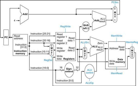
FIGURE 4.15 The datapath of Figure 4.11 with all necessary multiplexors and all control lines identified.
The control lines are shown in color. The ALU control block has also been added. The PC does not require a write control, since it is written once at the end of every clock cycle; the branch control logic determines whether it is written with the incremented PC or the branch target address.
Figure 4.15 shows seven single-bit control lines plus the 2-bit ALUOp control signal. We have already defined how the ALUOp control signal works, and it is useful to define what the seven other control signals do informally before we determine how to set these control signals during instruction execution. Figure 4.16 describes the function of these seven control lines.
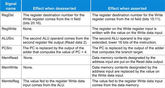
FIGURE 4.16 The effect of each of the seven control signals.
When the 1-bit control to a two-way multiplexor is asserted, the multiplexor selects the input corresponding to 1. Otherwise, if the control is deasserted, the multiplexor selects the 0 input. Remember that the state elements all have the clock as an implicit input and that the clock is used in controlling writes. Gating the clock externally to a state element can create timing problems. (See ![]() Appendix B for further discussion of this problem.)
Appendix B for further discussion of this problem.)
Now that we have looked at the function of each of the control signals, we can look at how to set them. The control unit can set all but one of the control signals based solely on the opcode field of the instruction. The PCSrc control line is the exception. That control line should be asserted if the instruction is branch on equal (a decision that the control unit can make) and the Zero output of the ALU, which is used for equality comparison, is asserted. To generate the PCSrc signal, we will need to AND together a signal from the control unit, which we call Branch, with the Zero signal out of the ALU.
These nine control signals (seven from Figure 4.16 and two for ALUOp) can now be set on the basis of six input signals to the control unit, which are the opcode bits 31 to 26. Figure 4.17 shows the datapath with the control unit and the control signals.
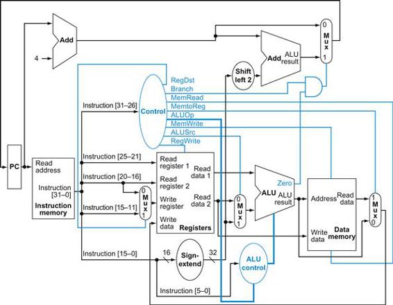
FIGURE 4.17 The simple datapath with the control unit.
The input to the control unit is the 6-bit opcode field from the instruction. The outputs of the control unit consist of three 1-bit signals that are used to control multiplexors (RegDst, ALUSrc, and MemtoReg), three signals for controlling reads and writes in the register file and data memory (RegWrite, MemRead, and MemWrite), a 1-bit signal used in determining whether to possibly branch (Branch), and a 2-bit control signal for the ALU (ALUOp). An AND gate is used to combine the branch control signal and the Zero output from the ALU; the AND gate output controls the selection of the next PC. Notice that PCSrc is now a derived signal, rather than one coming directly from the control unit. Thus, we drop the signal name in subsequent figures.
Before we try to write a set of equations or a truth table for the control unit, it will be useful to try to define the control function informally. Because the setting of the control lines depends only on the opcode, we define whether each control signal should be 0, 1, or don’t care (X) for each of the opcode values. Figure 4.18 defines how the control signals should be set for each opcode; this information follows directly from Figures 4.12, 4.16, and 4.17.
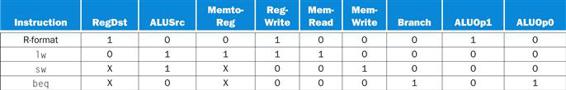
FIGURE 4.18 The setting of the control lines is completely determined by the opcode fields of the instruction.
The first row of the table corresponds to the R-format instructions (add, sub, AND, OR, and slt). For all these instructions, the source register fields are rs and rt, and the destination register field is rd; this defines how the signals ALUSrc and RegDst are set. Furthermore, an R-type instruction writes a register (RegWrite=1), but neither reads nor writes data memory. When the Branch control signal is 0, the PC is unconditionally replaced with PC+4; otherwise, the PC is replaced by the branch target if the Zero output of the ALU is also high. The ALUOp field for R-type instructions is set to 10 to indicate that the ALU control should be generated from the funct field. The second and third rows of this table give the control signal settings for lw and sw. These ALUSrc and ALUOp fields are set to perform the address calculation. The MemRead and MemWrite are set to perform the memory access. Finally, RegDst and RegWrite are set for a load to cause the result to be stored into the rt register. The branch instruction is similar to an R-format operation, since it sends the rs and rt registers to the ALU. The ALUOp field for branch is set for a subtract (ALU control=01), which is used to test for equality. Notice that the MemtoReg field is irrelevant when the RegWrite signal is 0: since the register is not being written, the value of the data on the register data write port is not used. Thus, the entry MemtoReg in the last two rows of the table is replaced with X for don’t care. Don’t cares can also be added to RegDst when RegWrite is 0. This type of don’t care must be added by the designer, since it depends on knowledge of how the datapath works.
Operation of the Datapath
With the information contained in Figures 4.16 and 4.18, we can design the control unit logic, but before we do that, let’s look at how each instruction uses the datapath. In the next few figures, we show the flow of three different instruction classes through the datapath. The asserted control signals and active datapath elements are highlighted in each of these. Note that a multiplexor whose control is 0 has a definite action, even if its control line is not highlighted. Multiple-bit control signals are highlighted if any constituent signal is asserted.
Figure 4.19 shows the operation of the datapath for an R-type instruction, such as add $t1,$t2,$t3. Although everything occurs in one clock cycle, we can think of four steps to execute the instruction; these steps are ordered by the flow of information:
1. The instruction is fetched, and the PC is incremented.
2. Two registers, $t2 and $t3, are read from the register file; also, the main control unit computes the setting of the control lines during this step.
3. The ALU operates on the data read from the register file, using the function code (bits 5:0, which is the funct field, of the instruction) to generate the ALU function.
4. The result from the ALU is written into the register file using bits 15:11 of the instruction to select the destination register ($t1).
FIGURE 4.19 The datapath in operation for an R-type instruction, such as add $t1,$t2,$t3.
The control lines, datapath units, and connections that are active are highlighted.
Similarly, we can illustrate the execution of a load word, such as
lw $t1, offset($t2)
in a style similar to Figure 4.19. Figure 4.20 shows the active functional units and asserted control lines for a load. We can think of a load instruction as operating in five steps (similar to the R-type executed in four):
1. An instruction is fetched from the instruction memory, and the PC is incremented.
2. A register ($t2) value is read from the register file.
3. The ALU computes the sum of the value read from the register file and the sign-extended, lower 16 bits of the instruction (offset).
4. The sum from the ALU is used as the address for the data memory.
5. The data from the memory unit is written into the register file; the register destination is given by bits 20:16 of the instruction ($t1).
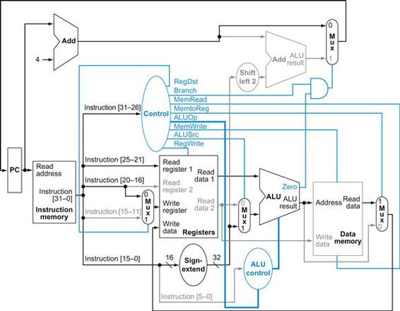
FIGURE 4.20 The datapath in operation for a load instruction.
The control lines, datapath units, and connections that are active are highlighted. A store instruction would operate very similarly. The main difference would be that the memory control would indicate a write rather than a read, the second register value read would be used for the data to store, and the operation of writing the data memory value to the register file would not occur.
Finally, we can show the operation of the branch-on-equal instruction, such as beq $t1, $t2, offset, in the same fashion. It operates much like an R-format instruction, but the ALU output is used to determine whether the PC is written with PC+4 or the branch target address. Figure 4.21 shows the four steps in execution:
1. An instruction is fetched from the instruction memory, and the PC is incremented.
2. Two registers, $t1 and $t2, are read from the register file.
3. The ALU performs a subtract on the data values read from the register file. The value of PC+4 is added to the sign-extended, lower 16 bits of the instruction (offset) shifted left by two; the result is the branch target address.
4. The Zero result from the ALU is used to decide which adder result to store into the PC.
FIGURE 4.21 The datapath in operation for a branch-on-equal instruction.
The control lines, datapath units, and connections that are active are highlighted. After using the register file and ALU to perform the compare, the Zero output is used to select the next program counter from between the two candidates.
Finalizing Control
Now that we have seen how the instructions operate in steps, let’s continue with the control implementation. The control function can be precisely defined using the contents of Figure 4.18. The outputs are the control lines, and the input is the 6-bit opcode field, Op [5:0]. Thus, we can create a truth table for each of the outputs based on the binary encoding of the opcodes.
Figure 4.22 shows the logic in the control unit as one large truth table that combines all the outputs and that uses the opcode bits as inputs. It completely specifies the control function, and we can implement it directly in gates in an automated fashion. We show this final step in Section D.2 in ![]() Appendix D.
Appendix D.
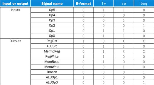
FIGURE 4.22 The control function for the simple single-cycle implementation is completely specified by this truth table.
The top half of the table gives the combinations of input signals that correspond to the four opcodes, one per column, that determine the control output settings. (Remember that Op [5:0] corresponds to bits 31:26 of the instruction, which is the op field.) The bottom portion of the table gives the outputs for each of the four opcodes. Thus, the output RegWrite is asserted for two different combinations of the inputs. If we consider only the four opcodes shown in this table, then we can simplify the truth table by using don’t cares in the input portion. For example, we can detect an R-format instruction with the expression ![]() , since this is sufficient to distinguish the R-format instructions from lw, sw, and beq. We do not take advantage of this simplification, since the rest of the MIPS opcodes are used in a full implementation.
, since this is sufficient to distinguish the R-format instructions from lw, sw, and beq. We do not take advantage of this simplification, since the rest of the MIPS opcodes are used in a full implementation.
Now that we have a single-cycle implementation of most of the MIPS core instruction set, let’s add the jump instruction to show how the basic datapath and control can be extended to handle other instructions in the instruction set.
single-cycle implementation
Also called single clock cycle implementation. An implementation in which an instruction is executed in one clock cycle. While easy to understand, it is too slow to be practical.
Implementing Jumps
Example
Figure 4.17 shows the implementation of many of the instructions we looked at in Chapter 2. One class of instructions missing is that of the jump instruction. Extend the datapath and control of Figure 4.17 to include the jump instruction. Describe how to set any new control lines.
Answer
The jump instruction, shown in Figure 4.23, looks somewhat like a branch instruction but computes the target PC differently and is not conditional. Like a branch, the low-order 2 bits of a jump address are always 00two. The next lower 26 bits of this 32-bit address come from the 26-bit immediate field in the instruction. The upper 4 bits of the address that should replace the PC come from the PC of the jump instruction plus 4. Thus, we can implement a jump by storing into the PC the concatenation of
■ the upper 4 bits of the current PC+4 (these are bits 31:28 of the sequentially following instruction address)
■ the 26-bit immediate field of the jump instruction
■ the bits 00two
![]()
FIGURE 4.23 Instruction format for the jump instruction (opcode=2).
The destination address for a jump instruction is formed by concatenating the upper 4 bits of the current PC+4 to the 26-bit address field in the jump instruction and adding 00 as the 2 low-order bits.
Figure 4.24 shows the addition of the control for jump added to Figure 4.17. An additional multiplexor is used to select the source for the new PC value, which is either the incremented PC (PC+4), the branch target PC, or the jump target PC. One additional control signal is needed for the additional multiplexor. This control signal, called Jump, is asserted only when the instruction is a jump—that is, when the opcode is 2.
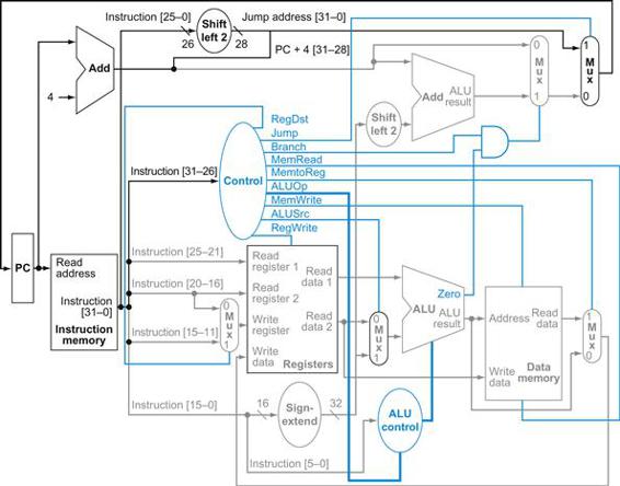
FIGURE 4.24 The simple control and datapath are extended to handle the jump instruction.
An additional multiplexor (at the upper right) is used to choose between the jump target and either the branch target or the sequential instruction following this one. This multiplexor is controlled by the jump control signal. The jump target address is obtained by shifting the lower 26 bits of the jump instruction left 2 bits, effectively adding 00 as the low-order bits, and then concatenating the upper 4 bits of PC+4 as the high-order bits, thus yielding a 32-bit address.
Why a Single-Cycle Implementation Is Not Used Today
Although the single-cycle design will work correctly, it would not be used in modern designs because it is inefficient. To see why this is so, notice that the clock cycle must have the same length for every instruction in this single-cycle design. Of course, the longest possible path in the processor determines the clock cycle. This path is almost certainly a load instruction, which uses five functional units in series: the instruction memory, the register file, the ALU, the data memory, and the register file. Although the CPI is 1 (see Chapter 1), the overall performance of a single-cycle implementation is likely to be poor, since the clock cycle is too long.
The penalty for using the single-cycle design with a fixed clock cycle is significant, but might be considered acceptable for this small instruction set. Historically, early computers with very simple instruction sets did use this implementation technique. However, if we tried to implement the floating-point unit or an instruction set with more complex instructions, this single-cycle design wouldn’t work well at all.
Because we must assume that the clock cycle is equal to the worst-case delay for all instructions, it’s useless to try implementation techniques that reduce the delay of the common case but do not improve the worst-case cycle time. A single-cycle implementation thus violates the great idea from Chapter 1 of making the common case fast.

In next section, we’ll look at another implementation technique, called pipelining, that uses a datapath very similar to the single-cycle datapath but is much more efficient by having a much higher throughput. Pipelining improves efficiency by executing multiple instructions simultaneously.
Check Yourself
Look at the control signals in Figure 4.22. Can you combine any together? Can any control signal output in the figure be replaced by the inverse of another? (Hint: take into account the don’t cares.) If so, can you use one signal for the other without adding an inverter?
4.5 An Overview of Pipelining
Never waste time.
American proverb
Pipelining is an implementation technique in which multiple instructions are overlapped in execution. Today, pipelining is nearly universal.
pipelining
An implementation technique in which multiple instructions are overlapped in execution, much like an assembly line.
This section relies heavily on one analogy to give an overview of the pipelining terms and issues. If you are interested in just the big picture, you should concentrate on this section and then skip to Sections 4.10 and 4.11 to see an introduction to the advanced pipelining techniques used in recent processors such as the Intel Core i7 and ARM Cortex-A8. If you are interested in exploring the anatomy of a pipelined computer, this section is a good introduction to Sections 4.6 through 4.9.
Anyone who has done a lot of laundry has intuitively used pipelining. The nonpipelined approach to laundry would be as follows:
1. Place one dirty load of clothes in the washer.
2. When the washer is finished, place the wet load in the dryer.
3. When the dryer is finished, place the dry load on a table and fold.
4. When folding is finished, ask your roommate to put the clothes away.
When your roommate is done, start over with the next dirty load.
The pipelined approach takes much less time, as Figure 4.25 shows. As soon as the washer is finished with the first load and placed in the dryer, you load the washer with the second dirty load. When the first load is dry, you place it on the table to start folding, move the wet load to the dryer, and put the next dirty load into the washer. Next you have your roommate put the first load away, you start folding the second load, the dryer has the third load, and you put the fourth load into the washer. At this point all steps—called stages in pipelining—are operating concurrently. As long as we have separate resources for each stage, we can pipeline the tasks.
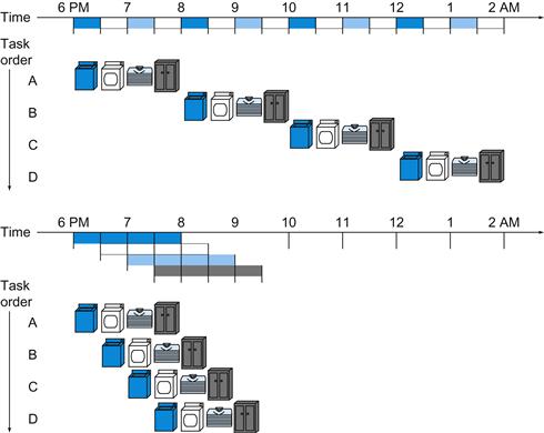
FIGURE 4.25 The laundry analogy for pipelining.
Ann, Brian, Cathy, and Don each have dirty clothes to be washed, dried, folded, and put away. The washer, dryer, “folder,” and “storer” each take 30 minutes for their task. Sequential laundry takes 8 hours for 4 loads of wash, while pipelined laundry takes just 3.5 hours. We show the pipeline stage of different loads over time by showing copies of the four resources on this two-dimensional time line, but we really have just one of each resource.
The pipelining paradox is that the time from placing a single dirty sock in the washer until it is dried, folded, and put away is not shorter for pipelining; the reason pipelining is faster for many loads is that everything is working in parallel, so more loads are finished per hour. Pipelining improves throughput of our laundry system. Hence, pipelining would not decrease the time to complete one load of laundry, but when we have many loads of laundry to do, the improvement in throughput decreases the total time to complete the work.
If all the stages take about the same amount of time and there is enough work to do, then the speed-up due to pipelining is equal to the number of stages in the pipeline, in this case four: washing, drying, folding, and putting away. Therefore, pipelined laundry is potentially four times faster than nonpipelined: 20 loads would take about 5 times as long as 1 load, while 20 loads of sequential laundry takes 20 times as long as 1 load. It’s only 2.3 times faster in Figure 4.25, because we only show 4 loads. Notice that at the beginning and end of the workload in the pipelined version in Figure 4.25, the pipeline is not completely full; this start-up and wind-down affects performance when the number of tasks is not large compared to the number of stages in the pipeline. If the number of loads is much larger than 4, then the stages will be full most of the time and the increase in throughput will be very close to 4.
The same principles apply to processors where we pipeline instruction-execution. MIPS instructions classically take five steps:
1. Fetch instruction from memory.
2. Read registers while decoding the instruction. The regular format of MIPS instructions allows reading and decoding to occur simultaneously.
3. Execute the operation or calculate an address.
4. Access an operand in data memory.
5. Write the result into a register.
Hence, the MIPS pipeline we explore in this chapter has five stages. The following example shows that pipelining speeds up instruction execution just as it speeds up the laundry.
Single-Cycle versus Pipelined Performance
Example
To make this discussion concrete, let’s create a pipeline. In this example, and in the rest of this chapter, we limit our attention to eight instructions: load word (lw), store word (sw), add (add), subtract (sub), AND (and), OR (or), set less than (slt), and branch on equal (beq).
Compare the average time between instructions of a single-cycle implementation, in which all instructions take one clock cycle, to a pipelined implementation. The operation times for the major functional units in this example are 200 ps for memory access, 200 ps for ALU operation, and 100 ps for register file read or write. In the single-cycle model, every instruction takes exactly one clock cycle, so the clock cycle must be stretched to accommodate the slowest instruction.
Answer
Figure 4.26 shows the time required for each of the eight instructions. The single-cycle design must allow for the slowest instruction—in Figure 4.26 it is lw—so the time required for every instruction is 800 ps. Similarly to Figure 4.25, Figure 4.27 compares nonpipelined and pipelined execution of three load word instructions. Thus, the time between the first and fourth instructions in the nonpipelined design is 3×800 ns or 2400 ps.
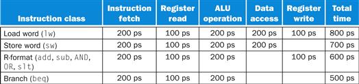
FIGURE 4.26 Total time for each instruction calculated from the time for each component.
This calculation assumes that the multiplexors, control unit, PC accesses, and sign extension unit have no delay.
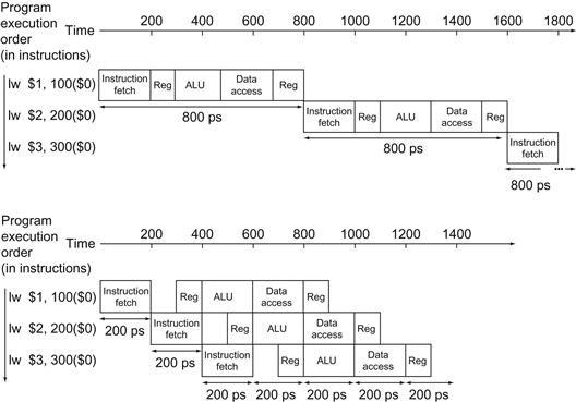
FIGURE 4.27 Single-cycle, nonpipelined execution in top versus pipelined execution in bottom.
Both use the same hardware components, whose time is listed in Figure 4.26. In this case, we see a fourfold speed-up on average time between instructions, from 800 ps down to 200 ps. Compare this figure to Figure 4.25. For the laundry, we assumed all stages were equal. If the dryer were slowest, then the dryer stage would set the stage time. The pipeline stage times of a computer are also limited by the slowest resource, either the ALU operation or the memory access. We assume the write to the register file occurs in the first half of the clock cycle and the read from the register file occurs in the second half. We use this assumption throughout this chapter.
All the pipeline stages take a single clock cycle, so the clock cycle must be long enough to accommodate the slowest operation. Just as the single-cycle design must take the worst-case clock cycle of 800 ps, even though some instructions can be as fast as 500 ps, the pipelined execution clock cycle must have the worst-case clock cycle of 200 ps, even though some stages take only 100 ps. Pipelining still offers a fourfold performance improvement: the time between the first and fourth instructions is 3×200 ps or 600 ps.
We can turn the pipelining speed-up discussion above into a formula. If the stages are perfectly balanced, then the time between instructions on the pipelined processor—assuming ideal conditions—is equal to
![]()
Under ideal conditions and with a large number of instructions, the speed-up from pipelining is approximately equal to the number of pipe stages; a five-stage pipeline is nearly five times faster.
The formula suggests that a five-stage pipeline should offer nearly a fivefold improvement over the 800 ps nonpipelined time, or a 160 ps clock cycle. The example shows, however, that the stages may be imperfectly balanced. Moreover, pipelining involves some overhead, the source of which will be clearer shortly. Thus, the time per instruction in the pipelined processor will exceed the minimum possible, and speed-up will be less than the number of pipeline stages.
Moreover, even our claim of fourfold improvement for our example is not reflected in the total execution time for the three instructions: it’s 1400 ps versus 2400 ps. Of course, this is because the number of instructions is not large. What would happen if we increased the number of instructions? We could extend the previous figures to 1,000,003 instructions. We would add 1,000,000 instructions in the pipelined example; each instruction adds 200 ps to the total execution time. The total execution time would be 1,000,000×200 ps+1400 ps, or 200,001,400 ps. In the nonpipelined example, we would add 1,000,000 instructions, each taking 800 ps, so total execution time would be 1,000,000×800 ps+2400 ps, or 800,002,400 ps. Under these conditions, the ratio of total execution times for real programs on nonpipelined to pipelined processors is close to the ratio of times between instructions:
![]()
Pipelining improves performance by increasing instruction throughput, as opposed to decreasing the execution time of an individual instruction, but instruction throughput is the important metric because real programs execute billions of instructions.
Designing Instruction Sets for Pipelining
Even with this simple explanation of pipelining, we can get insight into the design of the MIPS instruction set, which was designed for pipelined execution.
First, all MIPS instructions are the same length. This restriction makes it much easier to fetch instructions in the first pipeline stage and to decode them in the second stage. In an instruction set like the x86, where instructions vary from 1 byte to 15 bytes, pipelining is considerably more challenging. Recent implementations of the x86 architecture actually translate x86 instructions into simple operations that look like MIPS instructions and then pipeline the simple operations rather than the native x86 instructions! (See Section 4.10.)
Second, MIPS has only a few instruction formats, with the source register fields being located in the same place in each instruction. This symmetry means that the second stage can begin reading the register file at the same time that the hardware is determining what type of instruction was fetched. If MIPS instruction formats were not symmetric, we would need to split stage 2, resulting in six pipeline stages. We will shortly see the downside of longer pipelines.
Third, memory operands only appear in loads or stores in MIPS. This restriction means we can use the execute stage to calculate the memory address and then access memory in the following stage. If we could operate on the operands in memory, as in the x86, stages 3 and 4 would expand to an address stage, memory stage, and then execute stage.
Fourth, as discussed in Chapter 2, operands must be aligned in memory. Hence, we need not worry about a single data transfer instruction requiring two data memory accesses; the requested data can be transferred between processor and memory in a single pipeline stage.
Pipeline Hazards
There are situations in pipelining when the next instruction cannot execute in the following clock cycle. These events are called hazards, and there are three different types.
Hazards
The first hazard is called a structural hazard. It means that the hardware cannot support the combination of instructions that we want to execute in the same clock cycle. A structural hazard in the laundry room would occur if we used a washer-dryer combination instead of a separate washer and dryer, or if our roommate was busy doing something else and wouldn’t put clothes away. Our carefully scheduled pipeline plans would then be foiled.
structural hazard
When a planned instruction cannot execute in the proper clock cycle because the hardware does not support the combination of instructions that are set to execute.
As we said above, the MIPS instruction set was designed to be pipelined, making it fairly easy for designers to avoid structural hazards when designing a pipeline. Suppose, however, that we had a single memory instead of two memories. If the pipeline in Figure 4.27 had a fourth instruction, we would see that in the same clock cycle the first instruction is accessing data from memory while the fourth instruction is fetching an instruction from that same memory. Without two memories, our pipeline could have a structural hazard.
Data Hazards
Data hazards occur when the pipeline must be stalled because one step must wait for another to complete. Suppose you found a sock at the folding station for which no match existed. One possible strategy is to run down to your room and search through your clothes bureau to see if you can find the match. Obviously, while you are doing the search, loads that have completed drying and are ready to fold as well as those that have finished washing and are ready to dry.
data hazard
Also called a pipeline data hazard. When a planned instruction cannot execute in the proper clock cycle because data that is needed to execute the instruction is not yet available.
In a computer pipeline, data hazards arise from the dependence of one instruction on an earlier one that is still in the pipeline (a relationship that does not really exist when doing laundry). For example, suppose we have an add instruction followed immediately by a subtract instruction that uses the sum ($s0):
add $s0, $t0, $t1
sub $t2, $s0, $t3
Without intervention, a data hazard could severely stall the pipeline. The add instruction doesn’t write its result until the fifth stage, meaning that we would have to waste three clock cycles in the pipeline.
Although we could try to rely on compilers to remove all such hazards, the results would not be satisfactory. These dependences happen just too often and the delay is just too long to expect the compiler to rescue us from this dilemma.
The primary solution is based on the observation that we don’t need to wait for the instruction to complete before trying to resolve the data hazard. For the code sequence above, as soon as the ALU creates the sum for the add, we can supply it as an input for the subtract. Adding extra hardware to retrieve the missing item early from the internal resources is called forwarding or bypassing.
forwarding
Also called bypassing. A method of resolving a data hazard by retrieving the missing data element from internal buffers rather than waiting for it to arrive from programmer-visible registers or memory.
Forwarding with Two Instructions
Example
For the two instructions above, show what pipeline stages would be connected by forwarding. Use the drawing in Figure 4.28 to represent the datapath during the five stages of the pipeline. Align a copy of the datapath for each instruction, similar to the laundry pipeline in Figure 4.25.
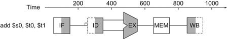
FIGURE 4.28 Graphical representation of the instruction pipeline, similar in spirit to the laundry pipeline in Figure 4.25.
Here we use symbols representing the physical resources with the abbreviations for pipeline stages used throughout the chapter. The symbols for the five stages: IF for the instruction fetch stage, with the box representing instruction memory; ID for the instruction decode/register file read stage, with the drawing showing the register file being read; EX for the execution stage, with the drawing representing the ALU; MEM for the memory access stage, with the box representing data memory; and WB for the write-back stage, with the drawing showing the register file being written. The shading indicates the element is used by the instruction. Hence, MEM has a white background because add does not access the data memory. Shading on the right half of the register file or memory means the element is read in that stage, and shading of the left half means it is written in that stage. Hence the right half of ID is shaded in the second stage because the register file is read, and the left half of WB is shaded in the fifth stage because the register file is written.
Answer
Figure 4.29 shows the connection to forward the value in $s0 after the execution stage of the add instruction as input to the execution stage of the sub instruction.
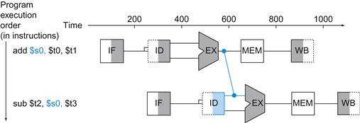
FIGURE 4.29 Graphical representation of forwarding.
The connection shows the forwarding path from the output of the EX stage of add to the input of the EX stage for sub, replacing the value from register $s0 read in the second stage of sub.
In this graphical representation of events, forwarding paths are valid only if the destination stage is later in time than the source stage. For example, there cannot be a valid forwarding path from the output of the memory access stage in the first instruction to the input of the execution stage of the following, since that would mean going backward in time.
Forwarding works very well and is described in detail in Section 4.7. It cannot prevent all pipeline stalls, however. For example, suppose the first instruction was a load of $s0 instead of an add. As we can imagine from looking at Figure 4.29, the desired data would be available only after the fourth stage of the first instruction in the dependence, which is too late for the input of the third stage of sub. Hence, even with forwarding, we would have to stall one stage for a load-use data hazard, as Figure 4.30 shows. This figure shows an important pipeline concept, officially called a pipeline stall, but often given the nickname bubble. We shall see stalls elsewhere in the pipeline. Section 4.7 shows how we can handle hard cases like these, using either hardware detection and stalls or software that reorders code to try to avoid load-use pipeline stalls, as this example illustrates.
load-use data hazard
A specific form of data hazard in which the data being loaded by a load instruction has not yet become available when it is needed by another instruction.
pipeline stall
Also called bubble. A stall initiated in order to resolve a hazard.
Reordering Code to Avoid Pipeline Stalls
Example
Consider the following code segment in C:
a = b + e;
c = b + f;
Here is the generated MIPS code for this segment, assuming all variables are in memory and are addressable as offsets from $t0:
lw $t1, 0($t0)
lw $t2, 4($t0)
add $t3, $t1,$t2
sw $t3, 12($t0)
lw $t4, 8($t0)
add $t5, $t1,$t4
sw $t5, 16($t0)
Find the hazards in the preceding code segment and reorder the instructions to avoid any pipeline stalls.
Answer
Both add instructions have a hazard because of their respective dependence on the immediately preceding lw instruction. Notice that bypassing eliminates several other potential hazards, including the dependence of the first add on the first lw and any hazards for store instructions. Moving up the third lw instruction to become the third instruction eliminates both hazards:
On a pipelined processor with forwarding, the reordered sequence will complete in two fewer cycles than the original version.
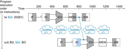
FIGURE 4.30 We need a stall even with forwarding when an R-format instruction following a load tries to use the data.
Without the stall, the path from memory access stage output to execution stage input would be going backward in time, which is impossible. This figure is actually a simplification, since we cannot know until after the subtract instruction is fetched and decoded whether or not a stall will be necessary. Section 4.7 shows the details of what really happens in the case of a hazard.
Forwarding yields another insight into the MIPS architecture, in addition to the four mentioned on page 277. Each MIPS instruction writes at most one result and does this in the last stage of the pipeline. Forwarding is harder if there are multiple results to forward per instruction or if there is a need to write a result early on in instruction execution.
Elaboration
The name “forwarding” comes from the idea that the result is passed forward from an earlier instruction to a later instruction. “Bypassing” comes from passing the result around the register file to the desired unit.
Control Hazards
The third type of hazard is called a control hazard, arising from the need to make a decision based on the results of one instruction while others are executing.
control hazard
Also called branch hazard. When the proper instruction cannot execute in the proper pipeline clock cycle because the instruction that was fetched is not the one that is needed; that is, the flow of instruction addresses is not what the pipeline expected.
Suppose our laundry crew was given the happy task of cleaning the uniforms of a football team. Given how filthy the laundry is, we need to determine whether the detergent and water temperature setting we select is strong enough to get the uniforms clean but not so strong that the uniforms wear out sooner. In our laundry pipeline, we have to wait until the second stage to examine the dry uniform to see if we need to change the washer setup or not. What to do?
Here is the first of two solutions to control hazards in the laundry room and its computer equivalent.
Stall: Just operate sequentially until the first batch is dry and then repeat until you have the right formula.
This conservative option certainly works, but it is slow.
The equivalent decision task in a computer is the branch instruction. Notice that we must begin fetching the instruction following the branch on the very next clock cycle. Nevertheless, the pipeline cannot possibly know what the next instruction should be, since it only just received the branch instruction from memory! Just as with laundry, one possible solution is to stall immediately after we fetch a branch, waiting until the pipeline determines the outcome of the branch and knows what instruction address to fetch from.
Let’s assume that we put in enough extra hardware so that we can test registers, calculate the branch address, and update the PC during the second stage of the pipeline (see Section 4.8 for details). Even with this extra hardware, the pipeline involving conditional branches would look like Figure 4.31. The lw instruction, executed if the branch fails, is stalled one extra 200 ps clock cycle before starting.
Performance of “Stall on Branch”
Example
Estimate the impact on the clock cycles per instruction (CPI) of stalling on branches. Assume all other instructions have a CPI of 1.
Answer
Figure 3.27 in Chapter 3 shows that branches are 17% of the instructions executed in SPECint2006. Since the other instructions run have a CPI of 1, and branches took one extra clock cycle for the stall, then we would see a CPI of 1.17 and hence a slowdown of 1.17 versus the ideal case.
FIGURE 4.31 Pipeline showing stalling on every conditional branch as solution to control hazards.
This example assumes the conditional branch is taken, and the instruction at the destination of the branch is the OR instruction. There is a one-stage pipeline stall, or bubble, after the branch. In reality, the process of creating a stall is slightly more complicated, as we will see in Section 4.8. The effect on performance, however, is the same as would occur if a bubble were inserted.
If we cannot resolve the branch in the second stage, as is often the case for longer pipelines, then we’d see an even larger slowdown if we stall on branches. The cost of this option is too high for most computers to use and motivates a second solution to the control hazard using one of our great ideas from Chapter 1:
Predict: If you’re pretty sure you have the right formula to wash uniforms, then just predict that it will work and wash the second load while waiting for the first load to dry.
This option does not slow down the pipeline when you are correct. When you are wrong, however, you need to redo the load that was washed while guessing the decision.
Computers do indeed use prediction to handle branches. One simple approach is to predict always that branches will be untaken. When you’re right, the pipeline proceeds at full speed. Only when branches are taken does the pipeline stall. Figure 4.32 shows such an example.

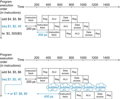
FIGURE 4.32 Predicting that branches are not taken as a solution to control hazard.
The top drawing shows the pipeline when the branch is not taken. The bottom drawing shows the pipeline when the branch is taken. As we noted in Figure 4.31, the insertion of a bubble in this fashion simplifies what actually happens, at least during the first clock cycle immediately following the branch. Section 4.8 will reveal the details.
A more sophisticated version of branch prediction would have some branches predicted as taken and some as untaken. In our analogy, the dark or home uniforms might take one formula while the light or road uniforms might take another. In the case of programming, at the bottom of loops are branches that jump back to the top of the loop. Since they are likely to be taken and they branch backward, we could always predict taken for branches that jump to an earlier address.
branch prediction
A method of resolving a branch hazard that assumes a given outcome for the branch and proceeds from that assumption rather than waiting to ascertain the actual outcome.
Such rigid approaches to branch prediction rely on stereotypical behavior and don’t account for the individuality of a specific branch instruction. Dynamic hardware predictors, in stark contrast, make their guesses depending on the behavior of each branch and may change predictions for a branch over the life of a program. Following our analogy, in dynamic prediction a person would look at how dirty the uniform was and guess at the formula, adjusting the next prediction depending on the success of recent guesses.
One popular approach to dynamic prediction of branches is keeping a history for each branch as taken or untaken, and then using the recent past behavior to predict the future. As we will see later, the amount and type of history kept have become extensive, with the result being that dynamic branch predictors can correctly predict branches with more than 90% accuracy (see Section 4.8). When the guess is wrong, the pipeline control must ensure that the instructions following the wrongly guessed branch have no effect and must restart the pipeline from the proper branch address. In our laundry analogy, we must stop taking new loads so that we can restart the load that we incorrectly predicted.
As in the case of all other solutions to control hazards, longer pipelines exacerbate the problem, in this case by raising the cost of misprediction. Solutions to control hazards are described in more detail in Section 4.8.
Elaboration
There is a third approach to the control hazard, called delayed decision. In our analogy, whenever you are going to make such a decision about laundry, just place a load of nonfootball clothes in the washer while waiting for football uniforms to dry. As long as you have enough dirty clothes that are not affected by the test, this solution works fine.
Called the delayed branch in computers, and mentioned above, this is the solution actually used by the MIPS architecture. The delayed branch always executes the next sequential instruction, with the branch taking place after that one instruction delay. It is hidden from the MIPS assembly language programmer because the assembler can automatically arrange the instructions to get the branch behavior desired by the programmer. MIPS software will place an instruction immediately after the delayed branch instruction that is not affected by the branch, and a taken branch changes the address of the instruction that follows this safe instruction. In our example, the add instruction before the branch in Figure 4.31 does not affect the branch and can be moved after the branch to fully hide the branch delay. Since delayed branches are useful when the branches are short, no processor uses a delayed branch of more than one cycle. For longer branch delays, hardware-based branch prediction is usually used.
Pipeline Overview Summary
Pipelining is a technique that exploits parallelism among the instructions in a sequential instruction stream. It has the substantial advantage that, unlike programming a multiprocessor, it is fundamentally invisible to the programmer.

In the next few sections of this chapter, we cover the concept of pipelining using the MIPS instruction subset from the single-cycle implementation in Section 4.4 and show a simplified version of its pipeline. We then look at the problems that pipelining introduces and the performance attainable under typical situations.
If you wish to focus more on the software and the performance implications of pipelining, you now have sufficient background to skip to Section 4.10. Section 4.10 introduces advanced pipelining concepts, such as superscalar and dynamic scheduling, and Section 4.11 examines the pipelines of recent microprocessors.
Alternatively, if you are interested in understanding how pipelining is implemented and the challenges of dealing with hazards, you can proceed to examine the design of a pipelined datapath and the basic control, explained in Section 4.6. You can then use this understanding to explore the implementation of forwarding and stalls in Section 4.7. You can then read Section 4.8 to learn more about solutions to branch hazards, and then see how exceptions are handled in Section 4.9.
Check Yourself
For each code sequence below, state whether it must stall, can avoid stalls using only forwarding, or can execute without stalling or forwarding.
|
Sequence 1 |
Sequence 2 |
Sequence 3 |
|
lw $t0, 0($t0) |
add $t1, $t0, $t0 |
addi $t1, $t0, #1 |
|
add $t1, $t0, $t0 |
addi $t2, $t0, #5 |
addi $t2, $t0, #2 |
|
addi $t4, $t1, #5 |
addi $t3, $t0, #2 |
|
|
addi $t3, $t0, #4 |
||
|
addi $t5, $t0, #5 |
Understanding Program Performance
Outside the memory system, the effective operation of the pipeline is usually the most important factor in determining the CPI of the processor and hence its performance. As we will see in Section 4.10, understanding the performance of a modern multiple-issue pipelined processor is complex and requires understanding more than just the issues that arise in a simple pipelined processor. Nonetheless, structural, data, and control hazards remain important in both simple pipelines and more sophisticated ones.
For modern pipelines, structural hazards usually revolve around the floating-point unit, which may not be fully pipelined, while control hazards are usually more of a problem in integer programs, which tend to have higher branch frequencies as well as less predictable branches. Data hazards can be performance bottlenecks in both integer and floating-point programs. Often it is easier to deal with data hazards in floating-point programs because the lower branch frequency and more regular memory access patterns allow the compiler to try to schedule instructions to avoid hazards. It is more difficult to perform such optimizations in integer programs that have less regular memory access, involving more use of pointers. As we will see in Section 4.10, there are more ambitious compiler and hardware techniques for reducing data dependences through scheduling.
The BIG Picture
Pipelining increases the number of simultaneously executing instructions and the rate at which instructions are started and completed. Pipelining does not reduce the time it takes to complete an individual instruction, also called the latency. For example, the five-stage pipeline still takes 5 clock cycles for the instruction to complete. In the terms used in Chapter 1, pipelining improves instruction throughput rather than individual instruction execution time or latency.
latency (pipeline)
The number of stages in a pipeline or the number of stages between two instructions during execution.
Instruction sets can either simplify or make life harder for pipeline designers, who must already cope with structural, control, and data hazards. Branch prediction and forwarding help make a computer fast while still getting the right answers.
4.6 Pipelined Datapath and Control
There is less in this than meets the eye.
Tallulah Bankhead, remark to Alexander Woollcott, 1922
Figure 4.33 shows the single-cycle datapath from Section 4.4 with the pipeline stages identified. The division of an instruction into five stages means a five-stage pipeline, which in turn means that up to five instructions will be in execution during any single clock cycle. Thus, we must separate the datapath into five pieces, with each piece named corresponding to a stage of instruction execution:
1. IF: Instruction fetch
2. ID: Instruction decode and register file read
3. EX: Execution or address calculation
4. MEM: Data memory access
5. WB: Write back
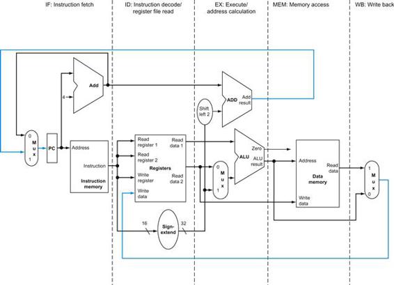
FIGURE 4.33 The single-cycle datapath from Section 4.4 (similar to Figure 4.17).
Each step of the instruction can be mapped onto the datapath from left to right. The only exceptions are the update of the PC and the write-back step, shown in color, which sends either the ALU result or the data from memory to the left to be written into the register file. (Normally we use color lines for control, but these are data lines.)
In Figure 4.33, these five components correspond roughly to the way the datapath is drawn; instructions and data move generally from left to right through the five stages as they complete execution. Returning to our laundry analogy, clothes get cleaner, drier, and more organized as they move through the line, and they never move backward.
There are, however, two exceptions to this left-to-right flow of instructions:
■ The write-back stage, which places the result back into the register file in the middle of the datapath
■ The selection of the next value of the PC, choosing between the incremented PC and the branch address from the MEM stage
Data flowing from right to left does not affect the current instruction; these reverse data movements influence only later instructions in the pipeline. Note that the first right-to-left flow of data can lead to data hazards and the second leads to control hazards.
One way to show what happens in pipelined execution is to pretend that each instruction has its own datapath, and then to place these datapaths on a timeline to show their relationship. Figure 4.34 shows the execution of the instructions in Figure 4.27 by displaying their private datapaths on a common timeline. We use a stylized version of the datapath in Figure 4.33 to show the relationships in Figure 4.34.
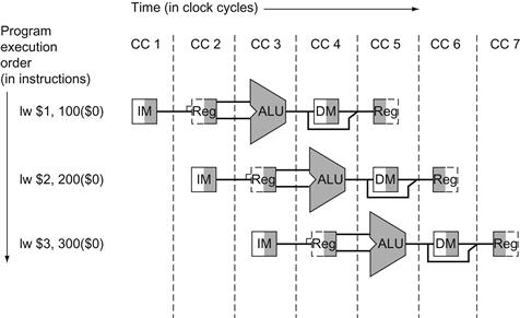
FIGURE 4.34 Instructions being executed using the single-cycle datapath in Figure 4.33, assuming pipelined execution.
Similar to Figures 4.28 through 4.30, this figure pretends that each instruction has its own datapath, and shades each portion according to use. Unlike those figures, each stage is labeled by the physical resource used in that stage, corresponding to the portions of the datapath in Figure 4.33. IM represents the instruction memory and the PC in the instruction fetch stage, Reg stands for the register file and sign extender in the instruction decode/register file read stage (ID), and so on. To maintain proper time order, this stylized datapath breaks the register file into two logical parts: registers read during register fetch (ID) and registers written during write back (WB). This dual use is represented by drawing the unshaded left half of the register file using dashed lines in the ID stage, when it is not being written, and the unshaded right half in dashed lines in the WB stage, when it is not being read. As before, we assume the register file is written in the first half of the clock cycle and the register file is read during the second half.
Figure 4.34 seems to suggest that three instructions need three datapaths. Instead, we add registers to hold data so that portions of a single datapath can be shared during instruction execution.
For example, as Figure 4.34 shows, the instruction memory is used during only one of the five stages of an instruction, allowing it to be shared by following instructions during the other four stages. To retain the value of an individual instruction for its other four stages, the value read from instruction memory must be saved in a register. Similar arguments apply to every pipeline stage, so we must place registers wherever there are dividing lines between stages in Figure 4.33. Returning to our laundry analogy, we might have a basket between each pair of stages to hold the clothes for the next step.
Figure 4.35 shows the pipelined datapath with the pipeline registers highlighted. All instructions advance during each clock cycle from one pipeline register to the next. The registers are named for the two stages separated by that register. For example, the pipeline register between the IF and ID stages is called IF/ID.
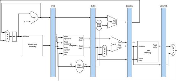
FIGURE 4.35 The pipelined version of the datapath in Figure 4.33.
The pipeline registers, in color, separate each pipeline stage. They are labeled by the stages that they separate; for example, the first is labeled IF/ID because it separates the instruction fetch and instruction decode stages. The registers must be wide enough to store all the data corresponding to the lines that go through them. For example, the IF/ID register must be 64 bits wide, because it must hold both the 32-bit instruction fetched from memory and the incremented 32-bit PC address. We will expand these registers over the course of this chapter, but for now the other three pipeline registers contain 128, 97, and 64 bits, respectively.
Notice that there is no pipeline register at the end of the write-back stage. All instructions must update some state in the processor—the register file, memory, or the PC—so a separate pipeline register is redundant to the state that is updated. For example, a load instruction will place its result in 1 of the 32 registers, and any later instruction that needs that data will simply read the appropriate register.
Of course, every instruction updates the PC, whether by incrementing it or by setting it to a branch destination address. The PC can be thought of as a pipeline register: one that feeds the IF stage of the pipeline. Unlike the shaded pipeline registers in Figure 4.35, however, the PC is part of the visible architectural state; its contents must be saved when an exception occurs, while the contents of the pipeline registers can be discarded. In the laundry analogy, you could think of the PC as corresponding to the basket that holds the load of dirty clothes before the wash step.
To show how the pipelining works, throughout this chapter we show sequences of figures to demonstrate operation over time. These extra pages would seem to require much more time for you to understand. Fear not; the sequences take much less time than it might appear, because you can compare them to see what changes occur in each clock cycle. Section 4.7 describes what happens when there are data hazards between pipelined instructions; ignore them for now.
Figures 4.36 through 4.38, our first sequence, show the active portions of the datapath highlighted as a load instruction goes through the five stages of pipelined execution. We show a load first because it is active in all five stages. As in Figures 4.28 through 4.30, we highlight the right half of registers or memory when they are being read and highlight the left half when they are being written.
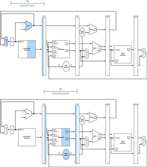
FIGURE 4.36 IF and ID: First and second pipe stages of an instruction, with the active portions of the datapath in Figure 4.35 highlighted.
The highlighting convention is the same as that used in Figure 4.28. As in Section 4.2, there is no confusion when reading and writing registers, because the contents change only on the clock edge. Although the load needs only the top register in stage 2, the processor doesn’t know what instruction is being decoded, so it sign-extends the 16-bit constant and reads both registers into the ID/EX pipeline register. We don’t need all three operands, but it simplifies control to keep all three.
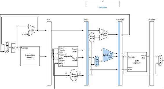
FIGURE 4.37 EX: The third pipe stage of a load instruction, highlighting the portions of the datapath in Figure 4.35 used in this pipe stage.
The register is added to the sign-extended immediate, and the sum is placed in the EX/MEM pipeline register.
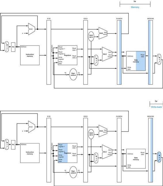
FIGURE 4.38 MEM and WB: The fourth and fifth pipe stages of a load instruction, highlighting the portions of the datapath in Figure 4.35 used in this pipe stage.
Data memory is read using the address in the EX/MEM pipeline registers, and the data is placed in the MEM/WB pipeline register. Next, data is read from the MEM/WB pipeline register and written into the register file in the middle of the datapath. Note: there is a bug in this design that is repaired in Figure 4.41.
We show the instruction abbreviation lw with the name of the pipe stage that is active in each figure. The five stages are the following:
1. Instruction fetch: The top portion of Figure 4.36 shows the instruction being read from memory using the address in the PC and then being placed in the IF/ID pipeline register. The PC address is incremented by 4 and then written back into the PC to be ready for the next clock cycle. This incremented address is also saved in the IF/ID pipeline register in case it is needed later for an instruction, such as beq. The computer cannot know which type of instruction is being fetched, so it must prepare for any instruction, passing potentially needed information down the pipeline.
2. Instruction decode and register file read: The bottom portion of Figure 4.36 shows the instruction portion of the IF/ID pipeline register supplying the 16-bit immediate field, which is sign-extended to 32 bits, and the register numbers to read the two registers. All three values are stored in the ID/EX pipeline register, along with the incremented PC address. We again transfer everything that might be needed by any instruction during a later clock cycle.
3. Execute or address calculation: Figure 4.37 shows that the load instruction reads the contents of register 1 and the sign-extended immediate from the ID/EX pipeline register and adds them using the ALU. That sum is placed in the EX/MEM pipeline register.
4. Memory access: The top portion of Figure 4.38 shows the load instruction reading the data memory using the address from the EX/MEM pipeline register and loading the data into the MEM/WB pipeline register.
5. Write-back: The bottom portion of Figure 4.38 shows the final step: reading the data from the MEM/WB pipeline register and writing it into the register file in the middle of the figure.
This walk-through of the load instruction shows that any information needed in a later pipe stage must be passed to that stage via a pipeline register. Walking through a store instruction shows the similarity of instruction execution, as well as passing the information for later stages. Here are the five pipe stages of the store instruction:
1. Instruction fetch: The instruction is read from memory using the address in the PC and then is placed in the IF/ID pipeline register. This stage occurs before the instruction is identified, so the top portion of Figure 4.36 works for store as well as load.
2. Instruction decode and register file read: The instruction in the IF/ID pipeline register supplies the register numbers for reading two registers and extends the sign of the 16-bit immediate. These three 32-bit values are all stored in the ID/EX pipeline register. The bottom portion of Figure 4.36 for load instructions also shows the operations of the second stage for stores. These first two stages are executed by all instructions, since it is too early to know the type of the instruction.
3. Execute and address calculation: Figure 4.39 shows the third step; the effective address is placed in the EX/MEM pipeline register.
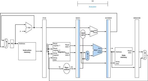
FIGURE 4.39 EX: The third pipe stage of a store instruction.
Unlike the third stage of the load instruction in Figure 4.37, the second register value is loaded into the EX/MEM pipeline register to be used in the next stage. Although it wouldn’t hurt to always write this second register into the EX/MEM pipeline register, we write the second register only on a store instruction to make the pipeline easier to understand.
4. Memory access: The top portion of Figure 4.40 shows the data being written to memory. Note that the register containing the data to be stored was read in an earlier stage and stored in ID/EX. The only way to make the data available during the MEM stage is to place the data into the EX/MEM pipeline register in the EX stage, just as we stored the effective address into EX/MEM.
FIGURE 4.40 MEM and WB: The fourth and fifth pipe stages of a store instruction.
In the fourth stage, the data is written into data memory for the store. Note that the data comes from the EX/MEM pipeline register and that nothing is changed in the MEM/WB pipeline register. Once the data is written in memory, there is nothing left for the store instruction to do, so nothing happens in stage 5.
5. Write-back: The bottom portion of Figure 4.40 shows the final step of the store. For this instruction, nothing happens in the write-back stage. Since every instruction behind the store is already in progress, we have no way to accelerate those instructions. Hence, an instruction passes through a stage even if there is nothing to do, because later instructions are already progressing at the maximum rate.
The store instruction again illustrates that to pass something from an early pipe stage to a later pipe stage, the information must be placed in a pipeline register; otherwise, the information is lost when the next instruction enters that pipeline stage. For the store instruction we needed to pass one of the registers read in the ID stage to the MEM stage, where it is stored in memory. The data was first placed in the ID/EX pipeline register and then passed to the EX/MEM pipeline register.
Load and store illustrate a second key point: each logical component of the datapath—such as instruction memory, register read ports, ALU, data memory, and register write port—can be used only within a single pipeline stage. Otherwise, we would have a structural hazard (see page 335). Hence these components, and their control, can be associated with a single pipeline stage.
Now we can uncover a bug in the design of the load instruction. Did you see it? Which register is changed in the final stage of the load? More specifically, which instruction supplies the write register number? The instruction in the IF/ID pipeline register supplies the write register number, yet this instruction occurs considerably after the load instruction!
Hence, we need to preserve the destination register number in the load instruction. Just as store passed the register contents from the ID/EX to the EX/MEM pipeline registers for use in the MEM stage, load must pass the register number from the ID/EX through EX/MEM to the MEM/WB pipeline register for use in the WB stage. Another way to think about the passing of the register number is that to share the pipelined datapath, we need to preserve the instruction read during the IF stage, so each pipeline register contains a portion of the instruction needed for that stage and later stages.
Figure 4.41 shows the correct version of the datapath, passing the write register number first to the ID/EX register, then to the EX/MEM register, and finally to the MEM/WB register. The register number is used during the WB stage to specify the register to be written. Figure 4.42 is a single drawing of the corrected datapath, highlighting the hardware used in all five stages of the load word instruction in Figures 4.36 through 4.38. See Section 4.8 for an explanation of how to make the branch instruction work as expected.
FIGURE 4.41 The corrected pipelined datapath to handle the load instruction properly.
The write register number now comes from the MEM/WB pipeline register along with the data. The register number is passed from the ID pipe stage until it reaches the MEM/WB pipeline register, adding five more bits to the last three pipeline registers. This new path is shown in color.
FIGURE 4.42 The portion of the datapath in Figure 4.41 that is used in all five stages of a load instruction.
Graphically Representing Pipelines
Pipelining can be difficult to understand, since many instructions are simultaneously executing in a single datapath in every clock cycle. To aid understanding, there are two basic styles of pipeline figures: multiple-clock-cycle pipeline diagrams, such as Figure 4.34 on page 288, and single-clock-cycle pipeline diagrams, such as Figures 4.36 through 4.40. The multiple-clock-cycle diagrams are simpler but do not contain all the details. For example, consider the following five-instruction sequence:
lw $10, 20($1)
sub $11, $2, $3
add $12, $3, $4
lw $13, 24($1)
add $14, $5, $6
Figure 4.43 shows the multiple-clock-cycle pipeline diagram for these instructions. Time advances from left to right across the page in these diagrams, and instructions advance from the top to the bottom of the page, similar to the laundry pipeline in Figure 4.25. A representation of the pipeline stages is placed in each portion along the instruction axis, occupying the proper clock cycles. These stylized datapaths represent the five stages of our pipeline graphically, but a rectangle naming each pipe stage works just as well. Figure 4.44 shows the more traditional version of the multiple-clock-cycle pipeline diagram. Note that Figure 4.43 shows the physical resources used at each stage, while Figure 4.44 uses the name of each stage.
FIGURE 4.43 Multiple-clock-cycle pipeline diagram of five instructions.
This style of pipeline representation shows the complete execution of instructions in a single figure. Instructions are listed in instruction execution order from top to bottom, and clock cycles move from left to right. Unlike Figure 4.28, here we show the pipeline registers between each stage. Figure 4.44 shows the traditional way to draw this diagram.
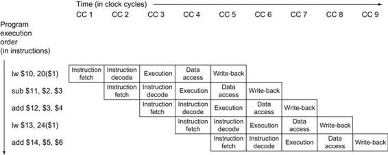
FIGURE 4.44 Traditional multiple-clock-cycle pipeline diagram of five instructions in Figure 4.43.
Single-clock-cycle pipeline diagrams show the state of the entire datapath during a single clock cycle, and usually all five instructions in the pipeline are identified by labels above their respective pipeline stages. We use this type of figure to show the details of what is happening within the pipeline during each clock cycle; typically, the drawings appear in groups to show pipeline operation over a sequence of clock cycles. We use multiple-clock-cycle diagrams to give overviews of pipelining situations. (![]() Section 4.13 gives more illustrations of single-clock diagrams if you would like to see more details about Figure 4.43.) A single-clock-cycle diagram represents a vertical slice through a set of multiple-clock-cycle diagrams, showing the usage of the datapath by each of the instructions in the pipeline at the designated clock cycle. For example, Figure 4.45 shows the single-clock-cycle diagram corresponding to clock cycle 5 of Figures 4.43 and 4.44. Obviously, the single-clock-cycle diagrams have more detail and take significantly more space to show the same number of clock cycles. The exercises ask you to create such diagrams for other code sequences.
Section 4.13 gives more illustrations of single-clock diagrams if you would like to see more details about Figure 4.43.) A single-clock-cycle diagram represents a vertical slice through a set of multiple-clock-cycle diagrams, showing the usage of the datapath by each of the instructions in the pipeline at the designated clock cycle. For example, Figure 4.45 shows the single-clock-cycle diagram corresponding to clock cycle 5 of Figures 4.43 and 4.44. Obviously, the single-clock-cycle diagrams have more detail and take significantly more space to show the same number of clock cycles. The exercises ask you to create such diagrams for other code sequences.
Check Yourself
A group of students were debating the efficiency of the five-stage pipeline when one student pointed out that not all instructions are active in every stage of the pipeline. After deciding to ignore the effects of hazards, they made the following four statements. Which ones are correct?
1. Allowing jumps, branches, and ALU instructions to take fewer stages than the five required by the load instruction will increase pipeline performance under all circumstances.
2. Trying to allow some instructions to take fewer cycles does not help, since the throughput is determined by the clock cycle; the number of pipe stages per instruction affects latency, not throughput.
3. You cannot make ALU instructions take fewer cycles because of the write-back of the result, but branches and jumps can take fewer cycles, so there is some opportunity for improvement.
4. Instead of trying to make instructions take fewer cycles, we should explore making the pipeline longer, so that instructions take more cycles, but the cycles are shorter. This could improve performance.
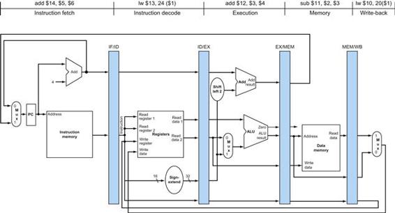
FIGURE 4.45 The single-clock-cycle diagram corresponding to clock cycle 5 of the pipeline in Figures 4.43 and 4.44.
As you can see, a single-clock-cycle figure is a vertical slice through a multiple-clock-cycle diagram.
Pipelined Control
In the 6600 Computer, perhaps even more than in any previous computer, the control system is the difference.
James Thornton, Design of a Computer: The Control Data 6600, 1970
Just as we added control to the single-cycle datapath in Section 4.3, we now add control to the pipelined datapath. We start with a simple design that views the problem through rose-colored glasses.
The first step is to label the control lines on the existing datapath. Figure 4.46 shows those lines. We borrow as much as we can from the control for the simple datapath in Figure 4.17. In particular, we use the same ALU control logic, branch logic, destination-register-number multiplexor, and control lines. These functions are defined in Figures 4.12, 4.16, and 4.18. We reproduce the key information in Figures 4.47through 4.49 on a single page to make the following discussion easier to follow.
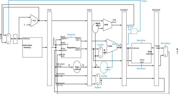
FIGURE 4.46 The pipelined datapath of Figure 4.41 with the control signals identified.
This datapath borrows the control logic for PC source, register destination number, and ALU control from Section 4.4. Note that we now need the 6-bit funct field (function code) of the instruction in the EX stage as input to ALU control, so these bits must also be included in the ID/EX pipeline register. Recall that these 6 bits are also the 6 least significant bits of the immediate field in the instruction, so the ID/EX pipeline register can supply them from the immediate field since sign extension leaves these bits unchanged.
As was the case for the single-cycle implementation, we assume that the PC is written on each clock cycle, so there is no separate write signal for the PC. By the same argument, there are no separate write signals for the pipeline registers (IF/ID, ID/EX, EX/MEM, and MEM/WB), since the pipeline registers are also written during each clock cycle.
To specify control for the pipeline, we need only set the control values during each pipeline stage. Because each control line is associated with a component active in only a single pipeline stage, we can divide the control lines into five groups according to the pipeline stage.
1. Instruction fetch: The control signals to read instruction memory and to write the PC are always asserted, so there is nothing special to control in this pipeline stage.
2. Instruction decode/register file read: As in the previous stage, the same thing happens at every clock cycle, so there are no optional control lines to set.
3. Execution/address calculation: The signals to be set are RegDst, ALUOp, and ALUSrc (see Figures 4.47 and 4.48). The signals select the Result register, the ALU operation, and either Read data 2 or a sign-extended immediate for the ALU.
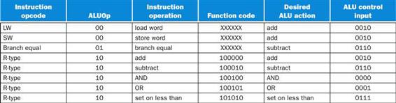
FIGURE 4.47 A copy of Figure 4.12.
This figure shows how the ALU control bits are set depending on the ALUOp control bits and the different function codes for the R-type instruction.
FIGURE 4.48 A copy of Figure 4.16.
The function of each of seven control signals is defined. The ALU control lines (ALUOp) are defined in the second column of Figure 4.47. When a 1-bit control to a 2-way multiplexor is asserted, the multiplexor selects the input corresponding to 1. Otherwise, if the control is deasserted, the multiplexor selects the 0 input. Note that PCSrc is controlled by an AND gate in Figure 4.46. If the Branch signal and the ALU Zero signal are both set, then PCSrc is 1; otherwise, it is 0. Control sets the Branch signal only during a beq instruction; otherwise, PCSrc is set to 0.
4. Memory access: The control lines set in this stage are Branch, MemRead, and MemWrite. The branch equal, load, and store instructions set these signals, respectively. Recall that PCSrc in Figure 4.48 selects the next sequential address unless control asserts Branch and the ALU result was 0.
5. Write-back: The two control lines are MemtoReg, which decides between sending the ALU result or the memory value to the register file, and RegWrite, which writes the chosen value.
Since pipelining the datapath leaves the meaning of the control lines unchanged, we can use the same control values. Figure 4.49 has the same values as in Section 4.4, but now the nine control lines are grouped by pipeline stage.
FIGURE 4.49 The values of the control lines are the same as in Figure 4.18, but they have been shuffled into three groups corresponding to the last three pipeline stages.
Implementing control means setting the nine control lines to these values in each stage for each instruction. The simplest way to do this is to extend the pipeline registers to include control information.
Since the control lines start with the EX stage, we can create the control information during instruction decode. Figure 4.50 above shows that these control signals are then used in the appropriate pipeline stage as the instruction moves down the pipeline, just as the destination register number for loads moves down the pipeline in Figure 4.41. Figure 4.51 shows the full datapath with the extended pipeline registers and with the control lines connected to the proper stage. (![]() Section 4.13 gives more examples of MIPS code executing on pipelined hardware using single-clock diagrams, if you would like to see more details.)
Section 4.13 gives more examples of MIPS code executing on pipelined hardware using single-clock diagrams, if you would like to see more details.)
FIGURE 4.50 The control lines for the final three stages.
Note that four of the nine control lines are used in the EX phase, with the remaining five control lines passed on to the EX/MEM pipeline register extended to hold the control lines; three are used during the MEM stage, and the last two are passed to MEM/WB for use in the WB stage.
FIGURE 4.51 The pipelined datapath of Figure 4.46, with the control signals connected to the control portions of the pipeline registers.
The control values for the last three stages are created during the instruction decode stage and then placed in the ID/EX pipeline register. The control lines for each pipe stage are used, and remaining control lines are then passed to the next pipeline stage.
4.7 Data Hazards: Forwarding versus Stalling
What do you mean, why’s it got to be built? It’s a bypass. You’ve got to build bypasses.
Douglas Adams, The Hitchhiker’s Guide to the Galaxy, 1979
The examples in the previous section show the power of pipelined execution and how the hardware performs the task. It’s now time to take off the rose-colored glasses and look at what happens with real programs. The instructions in Figures 4.43 through 4.45 were independent; none of them used the results calculated by any of the others. Yet in Section 4.5, we saw that data hazards are obstacles to pipelined execution.
Let’s look at a sequence with many dependences, shown in color:
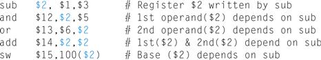
The last four instructions are all dependent on the result in register $2 of the first instruction. If register $2 had the value 10 before the subtract instruction and −20 afterwards, the programmer intends that −20 will be used in the following instructions that refer to register $2.
How would this sequence perform with our pipeline? Figure 4.52 illustrates the execution of these instructions using a multiple-clock-cycle pipeline representation. To demonstrate the execution of this instruction sequence in our current pipeline, the top of Figure 4.52 shows the value of register $2, which changes during the middle of clock cycle 5, when the sub instruction writes its result.
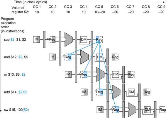
FIGURE 4.52 Pipelined dependences in a five-instruction sequence using simplified datapaths to show the dependences.
All the dependent actions are shown in color, and “CC 1” at the top of the figure means clock cycle 1. The first instruction writes into $2, and all the following instructions read $2. This register is written in clock cycle 5, so the proper value is unavailable before clock cycle 5. (A read of a register during a clock cycle returns the value written at the end of the first half of the cycle, when such a write occurs.) The colored lines from the top datapath to the lower ones show the dependences. Those that must go backward in time are pipeline data hazards.
The last potential hazard can be resolved by the design of the register file hardware: What happens when a register is read and written in the same clock cycle? We assume that the write is in the first half of the clock cycle and the read is in the second half, so the read delivers what is written. As is the case for many implementations of register files, we have no data hazard in this case.
Figure 4.52 shows that the values read for register $2 would not be the result of the sub instruction unless the read occurred during clock cycle 5 or later. Thus, the instructions that would get the correct value of −20 are add and sw; the AND and OR instructions would get the incorrect value 10! Using this style of drawing, such problems become apparent when a dependence line goes backward in time.
As mentioned in Section 4.5, the desired result is available at the end of the EX stage or clock cycle 3. When is the data actually needed by the AND and OR instructions? At the beginning of the EX stage, or clock cycles 4 and 5, respectively. Thus, we can execute this segment without stalls if we simply forward the data as soon as it is available to any units that need it before it is available to read from the register file.
How does forwarding work? For simplicity in the rest of this section, we consider only the challenge of forwarding to an operation in the EX stage, which may be either an ALU operation or an effective address calculation. This means that when an instruction tries to use a register in its EX stage that an earlier instruction intends to write in its WB stage, we actually need the values as inputs to the ALU.
A notation that names the fields of the pipeline registers allows for a more precise notation of dependences. For example, “ID/EX.RegisterRs” refers to the number of one register whose value is found in the pipeline register ID/EX; that is, the one from the first read port of the register file. The first part of the name, to the left of the period, is the name of the pipeline register; the second part is the name of the field in that register. Using this notation, the two pairs of hazard conditions are
1a. EX/MEM.RegisterRd=ID/EX.RegisterRs
1b. EX/MEM.RegisterRd=ID/EX.RegisterRt
2a. MEM/WB.RegisterRd=ID/EX.RegisterRs
2b. MEM/WB.RegisterRd=ID/EX.RegisterRt
The first hazard in the sequence on page 304 is on register $2, between the result of sub $2,$1,$3 and the first read operand of and $12,$2,$5. This hazard can be detected when the and instruction is in the EX stage and the prior instruction is in the MEM stage, so this is hazard 1a:
![]()
Dependence Detection
Example
Classify the dependences in this sequence from page 304:
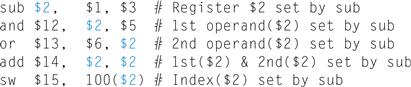
Answer
As mentioned above, the sub-and is a type 1a hazard. The remaining hazards are as follows:
■ The sub-or is a type 2b hazard:
![]()
■ The two dependences on sub-add are not hazards because the register file supplies the proper data during the ID stage of add.
■ There is no data hazard between sub and sw because sw reads $2 the clock cycle aftersub writes $2.
Because some instructions do not write registers, this policy is inaccurate; sometimes it would forward when it shouldn’t. One solution is simply to check to see if the RegWrite signal will be active: examining the WB control field of the pipeline register during the EX and MEM stages determines whether RegWrite is asserted. Recall that MIPS requires that every use of $0 as an operand must yield an operand value of 0. In the event that an instruction in the pipeline has $0 as its destination (for example, sll $0, $1, 2), we want to avoid forwarding its possibly nonzero result value. Not forwarding results destined for $0 frees the assembly programmer and the compiler of any requirement to avoid using $0 as a destination. The conditions above thus work properly as long we add EX/MEM.RegisterRd≠0 to the first hazard condition and MEM/WB.RegisterRd≠0 to the second.
Now that we can detect hazards, half of the problem is resolved—but we must still forward the proper data.
Figure 4.53 shows the dependences between the pipeline registers and the inputs to the ALU for the same code sequence as in Figure 4.52. The change is that the dependence begins from a pipeline register, rather than waiting for the WB stage to write the register file. Thus, the required data exists in time for later instructions, with the pipeline registers holding the data to be forwarded.
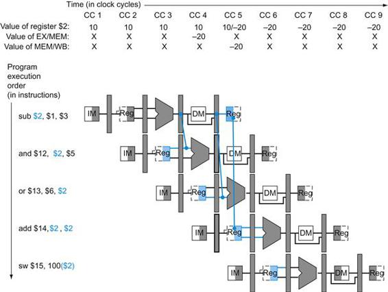
FIGURE 4.53 The dependences between the pipeline registers move forward in time, so it is possible to supply the inputs to the ALU needed by the AND instruction and OR instruction by forwarding the results found in the pipeline registers.
The values in the pipeline registers show that the desired value is available before it is written into the register file. We assume that the register file forwards values that are read and written during the same clock cycle, so the add does not stall, but the values come from the register file instead of a pipeline register. Register file “forwarding”—that is, the read gets the value of the write in that clock cycle—is why clock cycle 5 shows register $2 having the value 10 at the beginning and −20 at the end of the clock cycle. As in the rest of this section, we handle all forwarding except for the value to be stored by a store instruction.
If we can take the inputs to the ALU from any pipeline register rather than just ID/EX, then we can forward the proper data. By adding multiplexors to the input of the ALU, and with the proper controls, we can run the pipeline at full speed in the presence of these data dependences.
For now, we will assume the only instructions we need to forward are the four R-format instructions: add, sub, AND, and OR. Figure 4.54 shows a close-up of the ALU and pipeline register before and after adding forwarding. Figure 4.55 shows the values of the control lines for the ALU multiplexors that select either the register file values or one of the forwarded values.
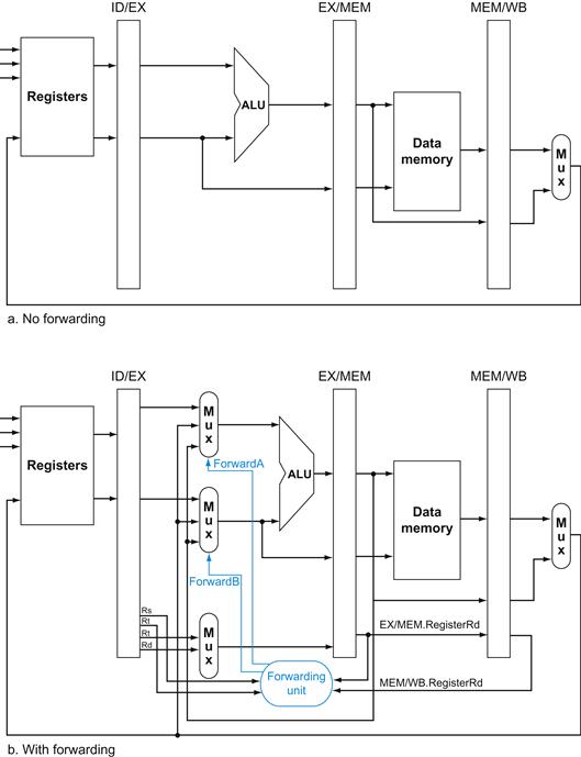
FIGURE 4.54 On the top are the ALU and pipeline registers before adding forwarding.
On the bottom, the multiplexors have been expanded to add the forwarding paths, and we show the forwarding unit. The new hardware is shown in color. This figure is a stylized drawing, however, leaving out details from the full datapath such as the sign extension hardware. Note that the ID/EX.RegisterRt field is shown twice, once to connect to the Mux and once to the forwarding unit, but it is a single signal. As in the earlier discussion, this ignores forwarding of a store value to a store instruction. Also note that this mechanism works for slt instructions as well.
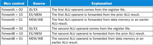
FIGURE 4.55 The control values for the forwarding multiplexors in Figure 4.54.
The signed immediate that is another input to the ALU is described in the Elaboration at the end of this section.
This forwarding control will be in the EX stage, because the ALU forwarding multiplexors are found in that stage. Thus, we must pass the operand register numbers from the ID stage via the ID/EX pipeline register to determine whether to forward values. We already have the rt field (bits 20–16). Before forwarding, the ID/EX register had no need to include space to hold the rs field. Hence, rs (bits 25–21) is added to ID/EX.
Let’s now write both the conditions for detecting hazards and the control signals to resolve them:
1. EX hazard:
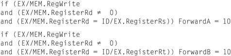
Note that the EX/MEM.RegisterRd field is the register destination for either an ALU instruction (which comes from the Rd field of the instruction) or a load (which comes from the Rt field).
This case forwards the result from the previous instruction to either input of the ALU. If the previous instruction is going to write to the register file, and the write register number matches the read register number of ALU inputs A or B, provided it is not register 0, then steer the multiplexor to pick the value instead from the pipeline register EX/MEM.
2. MEM hazard:
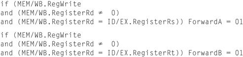
As mentioned above, there is no hazard in the WB stage, because we assume that the register file supplies the correct result if the instruction in the ID stage reads the same register written by the instruction in the WB stage. Such a register file performs another form of forwarding, but it occurs within the register file.
One complication is potential data hazards between the result of the instruction in the WB stage, the result of the instruction in the MEM stage, and the source operand of the instruction in the ALU stage. For example, when summing a vector of numbers in a single register, a sequence of instructions will all read and write to the same register:
add $1,$1,$2
add $1,$1,$3
add $1,$1,$4
. . .
In this case, the result is forwarded from the MEM stage because the result in the MEM stage is the more recent result. Thus, the control for the MEM hazard would be (with the additions highlighted):
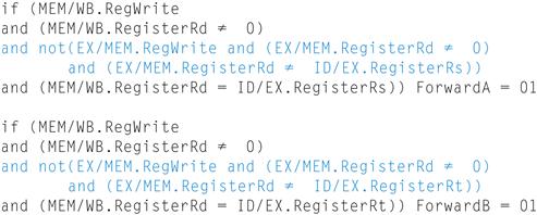
Figure 4.56 shows the hardware necessary to support forwarding for operations that use results during the EX stage. Note that the EX/MEM.RegisterRd field is the register destination for either an ALU instruction (which comes from the Rd field of the instruction) or a load (which comes from the Rt field).
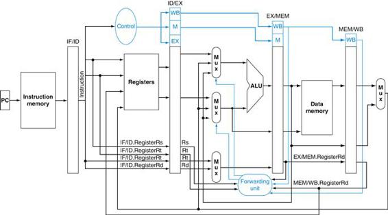
FIGURE 4.56 The datapath modified to resolve hazards via forwarding.
Compared with the datapath in Figure 4.51, the additions are the multiplexors to the inputs to the ALU. This figure is a more stylized drawing, however, leaving out details from the full datapath, such as the branch hardware and the sign extension hardware.
![]() Section 4.13 shows two pieces of MIPS code with hazards that cause forwarding, if you would like to see more illustrated examples using single-cycle pipeline drawings.
Section 4.13 shows two pieces of MIPS code with hazards that cause forwarding, if you would like to see more illustrated examples using single-cycle pipeline drawings.
Elaboration
Forwarding can also help with hazards when store instructions are dependent on other instructions. Since they use just one data value during the MEM stage, forwarding is easy. However, consider loads immediately followed by stores, useful when performing memory-to-memory copies in the MIPS architecture. Since copies are frequent, we need to add more forwarding hardware to make them run faster. If we were to redraw Figure 4.53, replacing the sub and AND instructions with lw and sw, we would see that it is possible to avoid a stall, since the data exists in the MEM/WB register of a load instruction in time for its use in the MEM stage of a store instruction. We would need to add forwarding into the memory access stage for this option. We leave this modification as an exercise to the reader.
In addition, the signed-immediate input to the ALU, needed by loads and stores, is missing from the datapath in Figure 4.56. Since central control decides between register and immediate, and since the forwarding unit chooses the pipeline register for a register input to the ALU, the easiest solution is to add a 2:1 multiplexor that chooses between the ForwardB multiplexor output and the signed immediate. Figure 4.57 shows this addition.
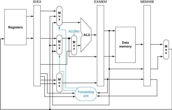
FIGURE 4.57 A close-up of the datapath in Figure 4.54 shows a 2:1 multiplexor, which has been added to select the signed immediate as an ALU input.
Data Hazards and Stalls
If at first you don’t succeed, redefine success.
Anonymous
As we said in Section 4.5, one case where forwarding cannot save the day is when an instruction tries to read a register following a load instruction that writes the same register. Figure 4.58 illustrates the problem. The data is still being read from memory in clock cycle 4 while the ALU is performing the operation for the following instruction. Something must stall the pipeline for the combination of load followed by an instruction that reads its result.
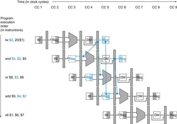
FIGURE 4.58 A pipelined sequence of instructions.
Since the dependence between the load and the following instruction (and) goes backward in time, this hazard cannot be solved by forwarding. Hence, this combination must result in a stall by the hazard detection unit.
Hence, in addition to a forwarding unit, we need a hazard detection unit. It operates during the ID stage so that it can insert the stall between the load and its use. Checking for load instructions, the control for the hazard detection unit is this single condition:
if (ID/EX.MemRead and ((ID/EX.RegisterRt=IF/ID.RegisterRs) or (ID/EX.RegisterRt=IF/ID.RegisterRt))) stall the pipeline
The first line tests to see if the instruction is a load: the only instruction that reads data memory is a load. The next two lines check to see if the destination register field of the load in the EX stage matches either source register of the instruction in the ID stage. If the condition holds, the instruction stalls one clock cycle. After this 1-cycle stall, the forwarding logic can handle the dependence and execution proceeds. (If there were no forwarding, then the instructions in Figure 4.58 would need another stall cycle.)
If the instruction in the ID stage is stalled, then the instruction in the IF stage must also be stalled; otherwise, we would lose the fetched instruction. Preventing these two instructions from making progress is accomplished simply by preventing the PC register and the IF/ID pipeline register from changing. Provided these registers are preserved, the instruction in the IF stage will continue to be read using the same PC, and the registers in the ID stage will continue to be read using the same instruction fields in the IF/ID pipeline register. Returning to our favorite analogy, it’s as if you restart the washer with the same clothes and let the dryer continue tumbling empty. Of course, like the dryer, the back half of the pipeline starting with the EX stage must be doing something; what it is doing is executing instructions that have no effect: nops.
nop
An instruction that does no operation to change state.
How can we insert these nops, which act like bubbles, into the pipeline? In Figure 4.49, we see that deasserting all nine control signals (setting them to 0) in the EX, MEM, and WB stages will create a “do nothing” or nop instruction. By identifying the hazard in the ID stage, we can insert a bubble into the pipeline by changing the EX, MEM, and WB control fields of the ID/EX pipeline register to 0. These benign control values are percolated forward at each clock cycle with the proper effect: no registers or memories are written if the control values are all 0.
Figure 4.59 shows what really happens in the hardware: the pipeline execution slot associated with the AND instruction is turned into a nop and all instructions beginning with the AND instruction are delayed one cycle. Like an air bubble in a water pipe, a stall bubble delays everything behind it and proceeds down the instruction pipe one stage each cycle until it exits at the end. In this example, the hazard forces the AND and OR instructions to repeat in clock cycle 4 what they did in clock cycle 3: AND reads registers and decodes, and OR is refetched from instruction memory. Such repeated work is what a stall looks like, but its effect is to stretch the time of the AND and OR instructions and delay the fetch of the add instruction.
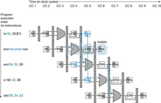
FIGURE 4.59 The way stalls are really inserted into the pipeline.
A bubble is inserted beginning in clock cycle 4, by changing the and instruction to a nop. Note that the and instruction is really fetched and decoded in clock cycles 2 and 3, but its EX stage is delayed until clock cycle 5 (versus the unstalled position in clock cycle 4). Likewise the OR instruction is fetched in clock cycle 3, but its ID stage is delayed until clock cycle 5 (versus the unstalled clock cycle 4 position). After insertion of the bubble, all the dependences go forward in time and no further hazards occur.
Figure 4.60 highlights the pipeline connections for both the hazard detection unit and the forwarding unit. As before, the forwarding unit controls the ALU multiplexors to replace the value from a general-purpose register with the value from the proper pipeline register. The hazard detection unit controls the writing of the PC and IF/ID registers plus the multiplexor that chooses between the real control values and all 0s. The hazard detection unit stalls and deasserts the control fields if the load-use hazard test above is true. ![]() Section 4.13 gives an example of MIPS code with hazards that causes stalling, illustrated using single-clock pipeline diagrams, if you would like to see more details.
Section 4.13 gives an example of MIPS code with hazards that causes stalling, illustrated using single-clock pipeline diagrams, if you would like to see more details.
The BIG Picture
Although the compiler generally relies upon the hardware to resolve hazards and thereby ensure correct execution, the compiler must understand the pipeline to achieve the best performance. Otherwise, unexpected stalls will reduce the performance of the compiled code.
Elaboration
Regarding the remark earlier about setting control lines to 0 to avoid writing registers or memory: only the signals RegWrite and MemWrite need be 0, while the other control signals can be don’t cares.
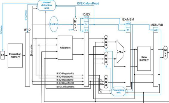
FIGURE 4.60 Pipelined control overview, showing the two multiplexors for forwarding, the hazard detection unit, and the forwarding unit.
Although the ID and EX stages have been simplified—the sign-extended immediate and branch logic are missing—this drawing gives the essence of the forwarding hardware requirements.
4.8 Control Hazards
There are a thousand hacking at the branches of evil to one who is striking at the root.
Henry David Thoreau, Walden, 1854
Thus far, we have limited our concern to hazards involving arithmetic operations and data transfers. However, as we saw in Section 4.5, there are also pipeline hazards involving branches. Figure 4.61 shows a sequence of instructions and indicates when the branch would occur in this pipeline. An instruction must be fetched at every clock cycle to sustain the pipeline, yet in our design the decision about whether to branch doesn’t occur until the MEM pipeline stage. As mentioned in Section 4.5, this delay in determining the proper instruction to fetch is called a control hazard or branch hazard, in contrast to the data hazards we have just examined.
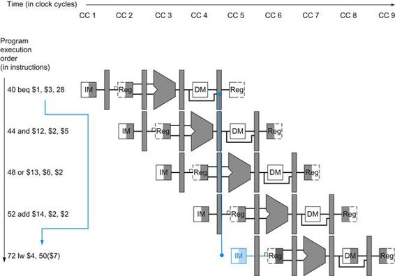
FIGURE 4.61 The impact of the pipeline on the branch instruction.
The numbers to the left of the instruction (40, 44, …) are the addresses of the instructions. Since the branch instruction decides whether to branch in the MEM stage—clock cycle 4 for the beq instruction above—the three sequential instructions that follow the branch will be fetched and begin execution. Without intervention, those three following instructions will begin execution before beq branches to lw at location 72. (Figure 4.31 assumed extra hardware to reduce the control hazard to one clock cycle; this figure uses the nonoptimized datapath.)
This section on control hazards is shorter than the previous sections on data hazards. The reasons are that control hazards are relatively simple to understand, they occur less frequently than data hazards, and there is nothing as effective against control hazards as forwarding is against data hazards. Hence, we use simpler schemes. We look at two schemes for resolving control hazards and one optimization to improve these schemes.
Assume Branch Not Taken
As we saw in Section 4.5, stalling until the branch is complete is too slow. One common improvement over branch stalling is to predict that the branch will not be taken and thus continue execution down the sequential instruction stream. If the branch is taken, the instructions that are being fetched and decoded must be discarded. Execution continues at the branch target. If branches are untaken half the time, and if it costs little to discard the instructions, this optimization halves the cost of control hazards.
To discard instructions, we merely change the original control values to 0s, much as we did to stall for a load-use data hazard. The difference is that we must also change the three instructions in the IF, ID, and EX stages when the branch reaches the MEM stage; for load-use stalls, we just change control to 0 in the ID stage and let them percolate through the pipeline. Discarding instructions, then, means we must be able to flush instructions in the IF, ID, and EX stages of the pipeline.
flush
To discard instructions in a pipeline, usually due to an unexpected event.
Reducing the Delay of Branches
One way to improve branch performance is to reduce the cost of the taken branch. Thus far, we have assumed the next PC for a branch is selected in the MEM stage, but if we move the branch execution earlier in the pipeline, then fewer instructions need be flushed. The MIPS architecture was designed to support fast single-cycle branches that could be pipelined with a small branch penalty. The designers observed that many branches rely only on simple tests (equality or sign, for example) and that such tests do not require a full ALU operation but can be done with at most a few gates. When a more complex branch decision is required, a separate instruction that uses an ALU to perform a comparison is required—a situation that is similar to the use of condition codes for branches (see Chapter 2).
Moving the branch decision up requires two actions to occur earlier: computing the branch target address and evaluating the branch decision. The easy part of this change is to move up the branch address calculation. We already have the PC value and the immediate field in the IF/ID pipeline register, so we just move the branch adder from the EX stage to the ID stage; of course, the branch target address calculation will be performed for all instructions, but only used when needed.
The harder part is the branch decision itself. For branch equal, we would compare the two registers read during the ID stage to see if they are equal. Equality can be tested by first exclusive ORing their respective bits and then ORing all the results. Moving the branch test to the ID stage implies additional forwarding and hazard detection hardware, since a branch dependent on a result still in the pipeline must still work properly with this optimization. For example, to implement branch on equal (and its inverse), we will need to forward results to the equality test logic that operates during ID. There are two complicating factors:
1. During ID, we must decode the instruction, decide whether a bypass to the equality unit is needed, and complete the equality comparison so that if the instruction is a branch, we can set the PC to the branch target address. Forwarding for the operands of branches was formerly handled by the ALU forwarding logic, but the introduction of the equality test unit in ID will require new forwarding logic. Note that the bypassed source operands of a branch can come from either the ALU/MEM or MEM/WB pipeline latches.
2. Because the values in a branch comparison are needed during ID but may be produced later in time, it is possible that a data hazard can occur and a stall will be needed. For example, if an ALU instruction immediately preceding a branch produces one of the operands for the comparison in the branch, a stall will be required, since the EX stage for the ALU instruction will occur after the ID cycle of the branch. By extension, if a load is immediately followed by a conditional branch that is on the load result, two stall cycles will be needed, as the result from the load appears at the end of the MEM cycle but is needed at the beginning of ID for the branch.
Despite these difficulties, moving the branch execution to the ID stage is an improvement, because it reduces the penalty of a branch to only one instruction if the branch is taken, namely, the one currently being fetched. The exercises explore the details of implementing the forwarding path and detecting the hazard.
To flush instructions in the IF stage, we add a control line, called IF.Flush, that zeros the instruction field of the IF/ID pipeline register. Clearing the register transforms the fetched instruction into a nop, an instruction that has no action and changes no state.
Pipelined Branch
Example
Show what happens when the branch is taken in this instruction sequence, assuming the pipeline is optimized for branches that are not taken and that we moved the branch execution to the ID stage:
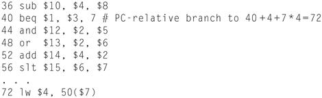
Answer
Figure 4.62 shows what happens when a branch is taken. Unlike Figure 4.61, there is only one pipeline bubble on a taken branch.
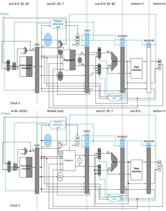
FIGURE 4.62 The ID stage of clock cycle 3 determines that a branch must be taken, so it selects 72 as the next PC address and zeros the instruction fetched for the next clock cycle.
Clock cycle 4 shows the instruction at location 72 being fetched and the single bubble or nop instruction in the pipeline as a result of the taken branch. (Since the nop is really sll $0, $0, 0, it’s arguable whether or not the ID stage in clock 4 should be highlighted.)
Dynamic Branch Prediction
Assuming a branch is not taken is one simple form of branch prediction. In that case, we predict that branches are untaken, flushing the pipeline when we are wrong. For the simple five-stage pipeline, such an approach, possibly coupled with compiler-based prediction, is probably adequate. With deeper pipelines, the branch penalty increases when measured in clock cycles. Similarly, with multiple issue (see Section 4.10), the branch penalty increases in terms of instructions lost. This combination means that in an aggressive pipeline, a simple static prediction scheme will probably waste too much performance. As we mentioned in Section 4.5, with more hardware it is possible to try to predict branch behavior during program execution.
One approach is to look up the address of the instruction to see if a branch was taken the last time this instruction was executed, and, if so, to begin fetching new instructions from the same place as the last time. This technique is called dynamic branch prediction.
dynamic branch prediction
Prediction of branches at runtime using runtime information.
One implementation of that approach is a branch prediction buffer or branch history table. A branch prediction buffer is a small memory indexed by the lower portion of the address of the branch instruction. The memory contains a bit that says whether the branch was recently taken or not.
branch prediction buffer
Also called branch history table. A small memory that is indexed by the lower portion of the address of the branch instruction and that contains one or more bits indicating whether the branch was recently taken or not.
This is the simplest sort of buffer; we don’t know, in fact, if the prediction is the right one—it may have been put there by another branch that has the same low-order address bits. However, this doesn’t affect correctness. Prediction is just a hint that we hope is correct, so fetching begins in the predicted direction. If the hint turns out to be wrong, the incorrectly predicted instructions are deleted, the prediction bit is inverted and stored back, and the proper sequence is fetched and executed.
This simple 1-bit prediction scheme has a performance shortcoming: even if a branch is almost always taken, we can predict incorrectly twice, rather than once, when it is not taken. The following example shows this dilemma.
Loops and Prediction
Example
Consider a loop branch that branches nine times in a row, then is not taken once. What is the prediction accuracy for this branch, assuming the prediction bit for this branch remains in the prediction buffer?
Answer
The steady-state prediction behavior will mispredict on the first and last loop iterations. Mispredicting the last iteration is inevitable since the prediction bit will indicate taken, as the branch has been taken nine times in a row at that point. The misprediction on the first iteration happens because the bit is flipped on prior execution of the last iteration of the loop, since the branch was not taken on that exiting iteration. Thus, the prediction accuracy for this branch that is taken 90% of the time is only 80% (two incorrect predictions and eight correct ones).
Ideally, the accuracy of the predictor would match the taken branch frequency for these highly regular branches. To remedy this weakness, 2-bit prediction schemes are often used. In a 2-bit scheme, a prediction must be wrong twice before it is changed. Figure 4.63 shows the finite-state machine for a 2-bit prediction scheme.
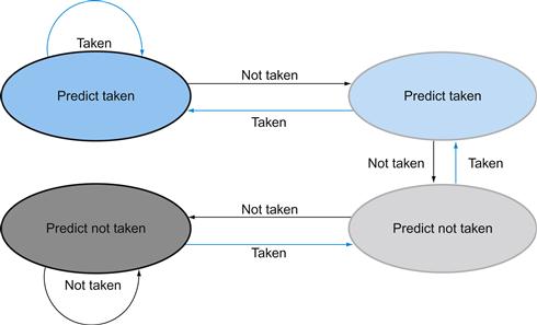
FIGURE 4.63 The states in a 2-bit prediction scheme.
By using 2 bits rather than 1, a branch that strongly favors taken or not taken—as many branches do—will be mispredicted only once. The 2 bits are used to encode the four states in the system. The 2-bit scheme is a general instance of a counter-based predictor, which is incremented when the prediction is accurate and decremented otherwise, and uses the mid-point of its range as the division between taken and not taken.
A branch prediction buffer can be implemented as a small, special buffer accessed with the instruction address during the IF pipe stage. If the instruction is predicted as taken, fetching begins from the target as soon as the PC is known; as mentioned on page 318, it can be as early as the ID stage. Otherwise, sequential fetching and executing continue. If the prediction turns out to be wrong, the prediction bits are changed as shown in Figure 4.63.
Elaboration
As we described in Section 4.5, in a five-stage pipeline we can make the control hazard a feature by redefining the branch. A delayed branch always executes the following instruction, but the second instruction following the branch will be affected by the branch.
Compilers and assemblers try to place an instruction that always executes after the branch in the branch delay slot. The job of the software is to make the successor instructions valid and useful. Figure 4.64 shows the three ways in which the branch delay slot can be scheduled.
branch delay slot
The slot directly after a delayed branch instruction, which in the MIPS architecture is filled by an instruction that does not affect the branch.
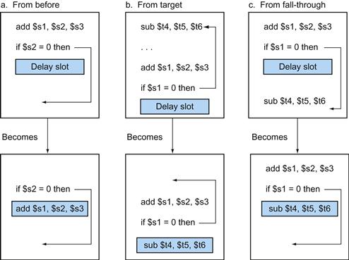
FIGURE 4.64 Scheduling the branch delay slot.
The top box in each pair shows the code before scheduling; the bottom box shows the scheduled code. In (a), the delay slot is scheduled with an independent instruction from before the branch. This is the best choice. Strategies (b) and (c) are used when (a) is not possible. In the code sequences for (b) and (c), the use of $s1 in the branch condition prevents the add instruction (whose destination is $s1) from being moved into the branch delay slot. In (b) the branch delay slot is scheduled from the target of the branch; usually the target instruction will need to be copied because it can be reached by another path. Strategy (b) is preferred when the branch is taken with high probability, such as a loop branch. Finally, the branch may be scheduled from the not-taken fall-through as in (c). To make this optimization legal for (b) or (c), it must be OK to execute the sub instruction when the branch goes in the unexpected direction. By “OK” we mean that the work is wasted, but the program will still execute correctly. This is the case, for example, if $t4 were an unused temporary register when the branch goes in the unexpected direction.
The limitations on delayed branch scheduling arise from (1) the restrictions on the instructions that are scheduled into the delay slots and (2) our ability to predict at compile time whether a branch is likely to be taken or not.
Delayed branching was a simple and effective solution for a five-stage pipeline issuing one instruction each clock cycle. As processors go to both longer pipelines and issuing multiple instructions per clock cycle (see Section 4.10), the branch delay becomes longer, and a single delay slot is insufficient. Hence, delayed branching has lost popularity compared to more expensive but more flexible dynamic approaches. Simultaneously, the growth in available transistors per chip has due to Moore’s Law made dynamic prediction relatively cheaper.

Elaboration
A branch predictor tells us whether or not a branch is taken, but still requires the calculation of the branch target. In the five-stage pipeline, this calculation takes one cycle, meaning that taken branches will have a 1-cycle penalty. Delayed branches are one approach to eliminate that penalty. Another approach is to use a cache to hold the destination program counter or destination instruction using a branch target buffer.
branch target buffer
A structure that caches the destination PC or destination instruction for a branch. It is usually organized as a cache with tags, making it more costly than a simple prediction buffer.
The 2-bit dynamic prediction scheme uses only information about a particular branch. Researchers noticed that using information about both a local branch, and the global behavior of recently executed branches together yields greater prediction accuracy for the same number of prediction bits. Such predictors are called correlating predictors. A typical correlating predictor might have two 2-bit predictors for each branch, with the choice between predictors made based on whether the last executed branch was taken or not taken. Thus, the global branch behavior can be thought of as adding additional index bits for the prediction lookup.
correlating predictor
A branch predictor that combines local behavior of a particular branch and global information about the behavior of some recent number of executed branches.
A more recent innovation in branch prediction is the use of tournament predictors. A tournament predictor uses multiple predictors, tracking, for each branch, which predictor yields the best results. A typical tournament predictor might contain two predictions for each branch index: one based on local information and one based on global branch behavior. A selector would choose which predictor to use for any given prediction. The selector can operate similarly to a 1-or 2-bit predictor, favoring whichever of the two predictors has been more accurate. Some recent microprocessors use such elaborate predictors.
tournament branch predictor
A branch predictor with multiple predictions for each branch and a selection mechanism that chooses which predictor to enable for a given branch.
Elaboration
One way to reduce the number of conditional branches is to add conditional move instructions. Instead of changing the PC with a conditional branch, the instruction conditionally changes the destination register of the move. If the condition fails, the move acts as a nop. For example, one version of the MIPS instruction set architecture has two new instructions called movn (move if not zero) and movz (move if zero). Thus, movn $8, $11, $4 copies the contents of register 11 into register 8, provided that the value in register 4 is nonzero; otherwise, it does nothing.
The ARMv7 instruction set has a condition field in most instructions. Hence, ARM programs could have fewer conditional branches than in MIPS programs.
Pipeline Summary
We started in the laundry room, showing principles of pipelining in an everyday setting. Using that analogy as a guide, we explained instruction pipelining step-by-step, starting with the single-cycle datapath and then adding pipeline registers, forwarding paths, data hazard detection, branch prediction, and flushing instructions on exceptions. Figure 4.65 shows the final evolved datapath and control. We now are ready for yet another control hazard: the sticky issue of exceptions.
Check Yourself
Consider three branch prediction schemes: predict not taken, predict taken, and dynamic prediction. Assume that they all have zero penalty when they predict correctly and two cycles when they are wrong. Assume that the average predict accuracy of the dynamic predictor is 90%. Which predictor is the best choice for the following branches?
1. A branch that is taken with 5% frequency
2. A branch that is taken with 95% frequency
3. A branch that is taken with 70% frequency
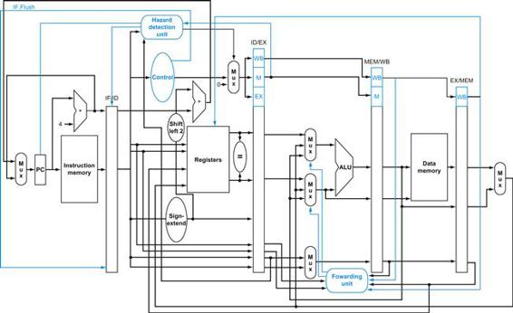
FIGURE 4.65 The final datapath and control for this chapter.
Note that this is a stylized figure rather than a detailed datapath, so it’s missing the ALUsrc Mux from Figure 4.57 and the multiplexor controls from Figure 4.51.
4.9 Exceptions
To make a computer with automatic program-interruption facilities behave [sequentially] was not an easy matter, because the number of instructions in various stages of processing when an interrupt signal occurs may be large.
Fred Brooks, Jr., Planning a Computer System: Project Stretch, 1962
Control is the most challenging aspect of processor design: it is both the hardest part to get right and the hardest part to make fast. One of the hardest parts of control is implementing exceptions and interrupts—events other than branches or jumps that change the normal flow of instruction execution. They were initially created to handle unexpected events from within the processor, like arithmetic overflow. The same basic mechanism was extended for I/O devices to communicate with the processor, as we will see in Chapter 6.
exception
Also called interrupt. An unscheduled event that disrupts program execution; used to detect overflow.
interrupt
An exception that comes from outside of the processor. (Some architectures use the term interrupt for all exceptions.)
Many architectures and authors do not distinguish between interrupts and exceptions, often using the older name interrupt to refer to both types of events. For example, the Intel x86 uses interrupt. We follow the MIPS convention, using the term exception to refer to any unexpected change in control flow without distinguishing whether the cause is internal or external; we use the term interrupt only when the event is externally caused. Here are five examples showing whether the situation is internally generated by the processor or externally generated:
|
Type of event |
From where? |
MIPS terminology |
|
I/O device request |
External |
Interrupt |
|
Invoke the operating system from user program |
Internal |
Exception |
|
Arithmetic overflow |
Internal |
Exception |
|
Using an undefined instruction |
Internal |
Exception |
|
Hardware malfunctions |
Either |
Exception or interrupt |
Many of the requirements to support exceptions come from the specific situation that causes an exception to occur. Accordingly, we will return to this topic in Chapter 5, when we will better understand the motivation for additional capabilities in the exception mechanism. In this section, we deal with the control implementation for detecting two types of exceptions that arise from the portions of the instruction set and implementation that we have already discussed.
Detecting exceptional conditions and taking the appropriate action is often on the critical timing path of a processor, which determines the clock cycle time and thus performance. Without proper attention to exceptions during design of the control unit, attempts to add exceptions to a complicated implementation can significantly reduce performance, as well as complicate the task of getting the design correct.
How Exceptions Are Handled in the MIPS Architecture
The two types of exceptions that our current implementation can generate are execution of an undefined instruction and an arithmetic overflow. We’ll use arithmetic overflow in the instruction add $1, $2, $1 as the example exception in the next few pages. The basic action that the processor must perform when an exception occurs is to save the address of the offending instruction in the exception program counter (EPC) and then transfer control to the operating system at some specified address.
The operating system can then take the appropriate action, which may involve providing some service to the user program, taking some predefined action in response to an overflow, or stopping the execution of the program and reporting an error. After performing whatever action is required because of the exception, the operating system can terminate the program or may continue its execution, using the EPC to determine where to restart the execution of the program. In Chapter 5, we will look more closely at the issue of restarting the execution.
For the operating system to handle the exception, it must know the reason for the exception, in addition to the instruction that caused it. There are two main methods used to communicate the reason for an exception. The method used in the MIPS architecture is to include a status register (called the Cause register), which holds a field that indicates the reason for the exception.
A second method, is to use vectored interrupts. In a vectored interrupt, the address to which control is transferred is determined by the cause of the exception. For example, to accommodate the two exception types listed above, we might define the following two exception vector addresses:
|
Exception type |
Exception vector address (in hex) |
|
Undefined instruction |
8000 0000hex |
|
Arithmetic overflow |
8000 0180hex |
vectored interrupt
An interrupt for which the address to which control is transferred is determined by the cause of the exception.
The operating system knows the reason for the exception by the address at which it is initiated. The addresses are separated by 32 bytes or eight instructions, and the operating system must record the reason for the exception and may perform some limited processing in this sequence. When the exception is not vectored, a single entry point for all exceptions can be used, and the operating system decodes the status register to find the cause.
We can perform the processing required for exceptions by adding a few extra registers and control signals to our basic implementation and by slightly extending control. Let’s assume that we are implementing the exception system used in the MIPS architecture, with the single entry point being the address 8000 0180hex. (Implementing vectored exceptions is no more difficult.) We will need to add two additional registers to the MIPS implementation:
■ EPC: A 32-bit register used to hold the address of the affected instruction. (Such a register is needed even when exceptions are vectored.)
■ Cause: A register used to record the cause of the exception. In the MIPS architecture, this register is 32 bits, although some bits are currently unused. Assume there is a five-bit field that encodes the two possible exception sources mentioned above, with 10 representing an undefined instruction and 12 representing arithmetic overflow.
Exceptions in a Pipelined Implementation
A pipelined implementation treats exceptions as another form of control hazard. For example, suppose there is an arithmetic overflow in an add instruction. Just as we did for the taken branch in the previous section, we must flush the instructions that follow the add instruction from the pipeline and begin fetching instructions from the new address. We will use the same mechanism we used for taken branches, but this time the exception causes the deasserting of control lines.
When we dealt with branch mispredict, we saw how to flush the instruction in the IF stage by turning it into a nop. To flush instructions in the ID stage, we use the multiplexor already in the ID stage that zeros control signals for stalls. A new control signal, called ID.Flush, is ORed with the stall signal from the hazard detection unit to flush during ID. To flush the instruction in the EX phase, we use a new signal called EX.Flush to cause new multiplexors to zero the control lines. To start fetching instructions from location 8000 0180hex, which is the MIPS exception address, we simply add an additional input to the PC multiplexor that sends 8000 0180hex to the PC. Figure 4.66 shows these changes.
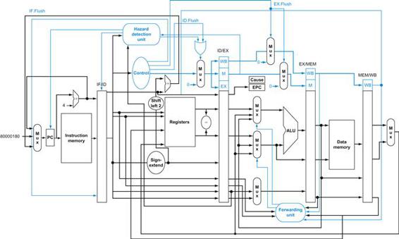
FIGURE 4.66 The datapath with controls to handle exceptions.
The key additions include a new input with the value 8000 0180hex in the multiplexor that supplies the new PC value; a Cause register to record the cause of the exception; and an Exception PC register to save the address of the instruction that caused the exception. The 8000 0180hex input to the multiplexor is the initial address to begin fetching instructions in the event of an exception. Although not shown, the ALU overflow signal is an input to the control unit.
This example points out a problem with exceptions: if we do not stop execution in the middle of the instruction, the programmer will not be able to see the original value of register $1 that helped cause the overflow because it will be clobbered as the Destination register of the add instruction. Because of careful planning, the overflow exception is detected during the EX stage; hence, we can use the EX.Flush signal to prevent the instruction in the EX stage from writing its result in the WB stage. Many exceptions require that we eventually complete the instruction that caused the exception as if it executed normally. The easiest way to do this is to flush the instruction and restart it from the beginning after the exception is handled.
The final step is to save the address of the offending instruction in the exception program counter (EPC). In reality, we save the address+4, so the exception handling routine must first subtract 4 from the saved value. Figure 4.66 shows a stylized version of the datapath, including the branch hardware and necessary accommodations to handle exceptions.
Exception in a Pipelined Computer
Example
Given this instruction sequence,
40hex sub $11, $2, $4
44hex and $12, $2, $5
48hex or $13, $2, $6
4Chex add $1, $2, $1
50hex slt $15, $6, $7
54hex lw $16, 50($7)
. . .
assume the instructions to be invoked on an exception begin like this:
80000180hex sw $26, 1000($0)
80000184hex sw $27, 1004($0)
. . .
Show what happens in the pipeline if an overflow exception occurs in the add instruction.
Answer
Figure 4.67 shows the events, starting with the add instruction in the EX stage. The overflow is detected during that phase, and 8000 0180hex is forced into the PC. Clock cycle 7 shows that the addand following instructions are flushed, and the first instruction of the exception code is fetched. Note that the address of the instruction following the add is saved: 4Chex+4=50hex.
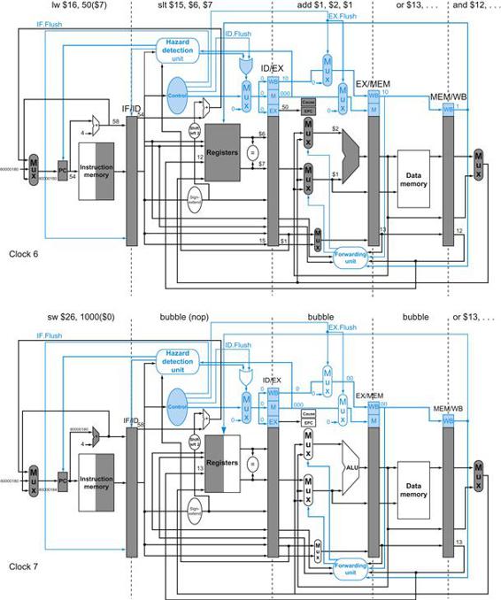
FIGURE 4.67 The result of an exception due to arithmetic overflow in the add instruction.
The overflow is detected during the EX stage of clock 6, saving the address following the add in the EPC register (4C+4=50hex). Overflow causes all the Flush signals to be set near the end of this clock cycle, deasserting control values (setting them to 0) for the add. Clock cycle 7 shows the instructions converted to bubbles in the pipeline plus the fetching of the first instruction of the exception routine—sw $25,1000($0)—from instruction location 8000 0180hex. Note that the AND and OR instructions, which are prior to the add, still complete. Although not shown, the ALU overflow signal is an input to the control unit.
We mentioned five examples of exceptions on page 326, and we will see others in Chapter 5. With five instructions active in any clock cycle, the challenge is to associate an exception with the appropriate instruction. Moreover, multiple exceptions can occur simultaneously in a single clock cycle. The solution is to prioritize the exceptions so that it is easy to determine which is serviced first. In most MIPS implementations, the hardware sorts exceptions so that the earliest instruction is interrupted.
I/O device requests and hardware malfunctions are not associated with a specific instruction, so the implementation has some flexibility as to when to interrupt the pipeline. Hence, the mechanism used for other exceptions works just fine.
The EPC captures the address of the interrupted instructions, and the MIPS Cause register records all possible exceptions in a clock cycle, so the exception software must match the exception to the instruction. An important clue is knowing in which pipeline stage a type of exception can occur. For example, an undefined instruction is discovered in the ID stage, and invoking the operating system occurs in the EX stage. Exceptions are collected in the Cause register in a pending exception field so that the hardware can interrupt based on later exceptions, once the earliest one has been serviced.
Hardware/Software Interface
The hardware and the operating system must work in conjunction so that exceptions behave as you would expect. The hardware contract is normally to stop the offending instruction in midstream, let all prior instructions complete, flush all following instructions, set a register to show the cause of the exception, save the address of the offending instruction, and then jump to a prearranged address. The operating system contract is to look at the cause of the exception and act appropriately. For an undefined instruction, hardware failure, or arithmetic overflow exception, the operating system normally kills the program and returns an indicator of the reason. For an I/O device request or an operating system service call, the operating system saves the state of the program, performs the desired task, and, at some point in the future, restores the program to continue execution. In the case of I/O device requests, we may often choose to run another task before resuming the task that requested the I/O, since that task may often not be able to proceed until the I/O is complete. This is why the ability to save and restore the state of any task is critical. One of the most important and frequent uses of exceptions is handling page faults and TLB exceptions; Chapter 5 describes these exceptions and their handling in more detail.
Elaboration
The difficulty of always associating the correct exception with the correct instruction in pipelined computers has led some computer designers to relax this requirement in noncritical cases. Such processors are said to have imprecise interrupts or imprecise exceptions. In the example above, PC would normally have 58hex at the start of the clock cycle after the exception is detected, even though the offending instruction is at address 4Chex. A processor with imprecise exceptions might put 58hex into EPC and leave it up to the operating system to determine which instruction caused the problem. MIPS and the vast majority of computers today support precise interrupts or precise exceptions. (One reason is to support virtual memory, which we shall see in Chapter 5.)
imprecise interrupt
Also called imprecise exception. Interrupts or exceptions in pipelined computers that are not associated with the exact instruction that was the cause of the interrupt or exception.
precise interrupt
Also called precise exception. An interrupt or exception that is always associated with the correct instruction in pipelined computers.
Elaboration
Although MIPS uses the exception entry address 8000 0180hex for almost all exceptions, it uses the address 8000 0000hex to improve performance of the exception handler for TLB-miss exceptions (see Chapter 5).
Check Yourself
Which exception should be recognized first in this sequence?
1. add $1, $2, $1 # arithmetic overflow
2. XXX $1, $2, $1 # undefined instruction
3. sub $1, $2, $1 # hardware error
4.10 Parallelism via Instructions
Be forewarned: this section is a brief overview of fascinating but advanced topics. If you want to learn more details, you should consult our more advanced book, Computer Architecture: A Quantitative Approach, fifth edition, where the material covered in the next 13 pages is expanded to almost 200 pages (including Appendices)!
Pipelining exploits the potential parallelism among instructions. This parallelism is called instruction-level parallelism (ILP). There are two primary methods for increasing the potential amount of instruction-level parallelism. The first is increasing the depth of the pipeline to overlap more instructions. Using our laundry analogy and assuming that the washer cycle was longer than the others were, we could divide our washer into three machines that perform the wash, rinse, and spin steps of a traditional washer. We would then move from a four-stage to a six-stage pipeline. To get the full speedup, we need to rebalance the remaining steps so they are the same length, in processors or in laundry. The amount of parallelism being exploited is higher, since there are more operations being overlapped. Performance is potentially greater since the clock cycle can be shorter.
instruction-level parallelism
The parallelism among instructions.
Another approach is to replicate the internal components of the computer so that it can launch multiple instructions in every pipeline stage. The general name for this technique is multiple issue. A multiple-issue laundry would replace our household washer and dryer with, say, three washers and three dryers. You would also have to recruit more assistants to fold and put away three times as much laundry in the same amount of time. The downside is the extra work to keep all the machines busy and transferring the loads to the next pipeline stage.
multiple issue
A scheme whereby multiple instructions are launched in one clock cycle.
Launching multiple instructions per stage allows the instruction execution rate to exceed the clock rate or, stated alternatively, the CPI to be less than 1. As mentioned in Chapter 1, it is sometimes useful to flip the metric and use IPC, or instructions per clock cycle. Hence, a 4 GHz four-way multiple-issue microprocessor can execute a peak rate of 16 billion instructions per second and have a best-case CPI of 0.25, or an IPC of 4. Assuming a five-stage pipeline, such a processor would have 20 instructions in execution at any given time. Today’s high-end microprocessors attempt to issue from three to six instructions in every clock cycle. Even moderate designs will aim at an IPC of 2. There are typically, however, many constraints on what types of instructions may be executed simultaneously, and what happens when dependences arise.
There are two major ways to implement a multiple-issue processor, with the major difference being the division of work between the compiler and the hardware. Because the division of work dictates whether decisions are being made statically (that is, at compile time) or dynamically (that is, during execution), the approaches are sometimes called static multiple issue and dynamic multiple issue. As we will see, both approaches have other, more commonly used names, which may be less precise or more restrictive.
static multiple issue
An approach to implementing a multiple-issue processor where many decisions are made by the compiler before execution.
dynamic multiple issue
An approach to implementing a multiple-issue processor where many decisions are made during execution by the processor.
There are two primary and distinct responsibilities that must be dealt with in a multiple-issue pipeline:
1. Packaging instructions into issue slots: how does the processor determine how many instructions and which instructions can be issued in a given clock cycle? In most static issue processors, this process is at least partially handled by the compiler; in dynamic issue designs, it is normally dealt with at runtime by the processor, although the compiler will often have already tried to help improve the issue rate by placing the instructions in a beneficial order.
2. Dealing with data and control hazards: in static issue processors, the compiler handles some or all of the consequences of data and control hazards statically. In contrast, most dynamic issue processors attempt to alleviate at least some classes of hazards using hardware techniques operating at execution time.
issue slots
The positions from which instructions could issue in a given clock cycle; by analogy, these correspond to positions at the starting blocks for a sprint.
Although we describe these as distinct approaches, in reality one approach often borrows techniques from the other, and neither approach can claim to be perfectly pure.
The Concept of Speculation
One of the most important methods for finding and exploiting more ILP is speculation. Based on the great idea of prediction, speculation is an approach that allows the compiler or the processor to “guess” about the properties of an instruction, so as to enable execution to begin for other instructions that may depend on the speculated instruction. For example, we might speculate on the outcome of a branch, so that instructions after the branch could be executed earlier. Another example is that we might speculate that a store that precedes a load does not refer to the same address, which would allow the load to be executed before the store. The difficulty with speculation is that it may be wrong. So, any speculation mechanism must include both a method to check if the guess was right and a method to unroll or back out the effects of the instructions that were executed speculatively. The implementation of this back-out capability adds complexity.
speculation
An approach whereby the compiler or processor guesses the outcome of an instruction to remove it as a dependence in executing other instructions.
Speculation may be done in the compiler or by the hardware. For example, the compiler can use speculation to reorder instructions, moving an instruction across a branch or a load across a store. The processor hardware can perform the same transformation at runtime using techniques we discuss later in this section.
The recovery mechanisms used for incorrect speculation are rather different. In the case of speculation in software, the compiler usually inserts additional instructions that check the accuracy of the speculation and provide a fix-up routine to use when the speculation is incorrect. In hardware speculation, the processor usually buffers the speculative results until it knows they are no longer speculative. If the speculation is correct, the instructions are completed by allowing the contents of the buffers to be written to the registers or memory. If the speculation is incorrect, the hardware flushes the buffers and re-executes the correct instruction sequence.
Speculation introduces one other possible problem: speculating on certain instructions may introduce exceptions that were formerly not present. For example, suppose a load instruction is moved in a speculative manner, but the address it uses is not legal when the speculation is incorrect. The result would be that an exception that should not have occurred will occur. The problem is complicated by the fact that if the load instruction were not speculative, then the exception must occur! In compiler-based speculation, such problems are avoided by adding special speculation support that allows such exceptions to be ignored until it is clear that they really should occur. In hardware-based speculation, exceptions are simply buffered until it is clear that the instruction causing them is no longer speculative and is ready to complete; at that point the exception is raised, and nor-mal exception handling proceeds.
Since speculation can improve performance when done properly and decrease performance when done carelessly, significant effort goes into deciding when it is appropriate to speculate. Later in this section, we will examine both static and dynamic techniques for speculation.
Static Multiple Issue
Static multiple-issue processors all use the compiler to assist with packaging instructions and handling hazards. In a static issue processor, you can think of the set of instructions issued in a given clock cycle, which is called an issue packet, as one large instruction with multiple operations. This view is more than an analogy. Since a static multiple-issue processor usually restricts what mix of instructions can be initiated in a given clock cycle, it is useful to think of the issue packet as a single instruction allowing several operations in certain predefined fields. This view led to the original name for this approach: Very Long Instruction Word (VLIW).
issue packet
The set of instructions that issues together in one clock cycle; the packet may be determined statically by the compiler or dynamically by the processor.
Very Long Instruction Word (VLIW)
A style of instruction set architecture that launches many operations that are defined to be independent in a single wide instruction, typically with many separate opcode fields.
Most static issue processors also rely on the compiler to take on some responsibility for handling data and control hazards. The compiler’s responsibilities may include static branch prediction and code scheduling to reduce or prevent all hazards. Let’s look at a simple static issue version of a MIPS processor, before we describe the use of these techniques in more aggressive processors.
An Example: Static Multiple Issue with the MIPS ISA
To give a flavor of static multiple issue, we consider a simple two-issue MIPS processor, where one of the instructions can be an integer ALU operation or branch and the other can be a load or store. Such a design is like that used in some embedded MIPS processors. Issuing two instructions per cycle will require fetching and decoding 64 bits of instructions. In many static multiple-issue processors, and essentially all VLIW processors, the layout of simultaneously issuing instructions is restricted to simplify the decoding and instruction issue. Hence, we will require that the instructions be paired and aligned on a 64-bit boundary, with the ALU or branch portion appearing first. Furthermore, if one instruction of the pair cannot be used, we require that it be replaced with a nop. Thus, the instructions always issue in pairs, possibly with a nop in one slot. Figure 4.68 shows how the instructions look as they go into the pipeline in pairs.
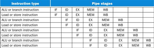
FIGURE 4.68 Static two-issue pipeline in operation.
The ALU and data transfer instructions are issued at the same time. Here we have assumed the same five-stage structure as used for the single-issue pipeline. Although this is not strictly necessary, it does have some advantages. In particular, keeping the register writes at the end of the pipeline simplifies the handling of exceptions and the maintenance of a precise exception model, which become more difficult in multiple-issue processors.
Static multiple-issue processors vary in how they deal with potential data and control hazards. In some designs, the compiler takes full responsibility for removing all hazards, scheduling the code and inserting no-ops so that the code executes without any need for hazard detection or hardware-generated stalls. In others, the hardware detects data hazards and generates stalls between two issue packets, while requiring that the compiler avoid all dependences within an instruction pair. Even so, a hazard generally forces the entire issue packet containing the dependent instruction to stall. Whether the software must handle all hazards or only try to reduce the fraction of hazards between separate issue packets, the appearance of having a large single instruction with multiple operations is reinforced. We will assume the second approach for this example.
To issue an ALU and a data transfer operation in parallel, the first need for additional hardware—beyond the usual hazard detection and stall logic—is extra ports in the register file (see Figure 4.69). In one clock cycle we may need to read two registers for the ALU operation and two more for a store, and also one write port for an ALU operation and one write port for a load. Since the ALU is tied up for the ALU operation, we also need a separate adder to calculate the effective address for data transfers. Without these extra resources, our two-issue pipeline would be hindered by structural hazards.
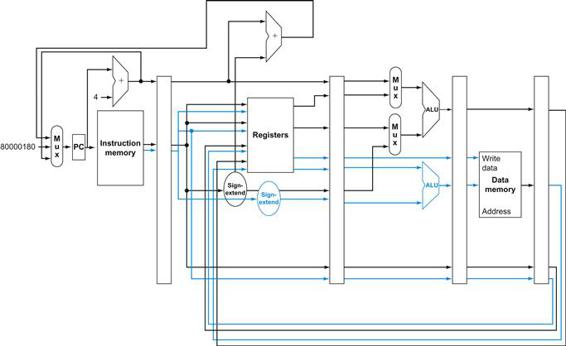
FIGURE 4.69 A static two-issue datapath.
The additions needed for double issue are highlighted: another 32 bits from instruction memory, two more read ports and one more write port on the register file, and another ALU. Assume the bottom ALU handles address calculations for data transfers and the top ALU handles everything else.
Clearly, this two-issue processor can improve performance by up to a factor of 2. Doing so, however, requires that twice as many instructions be overlapped in execution, and this additional overlap increases the relative performance loss from data and control hazards. For example, in our simple five-stage pipeline, loads have a use latency of one clock cycle, which prevents one instruction from using the result without stalling. In the two-issue, five-stage pipeline the result of a load instruction cannot be used on the next clock cycle. This means that the next two instructions cannot use the load result without stalling. Furthermore, ALU instructions that had no use latency in the simple five-stage pipeline now have a one-instruction use latency, since the results cannot be used in the paired load or store. To effectively exploit the parallelism available in a multiple-issue processor, more ambitious compiler or hardware scheduling techniques are needed, and static multiple issue requires that the compiler take on this role.
use latency
Number of clock cycles between a load instruction and an instruction that can use the result of the load without stalling the pipeline.
Simple Multiple-Issue Code Scheduling
Example
How would this loop be scheduled on a static two-issue pipeline for MIPS?
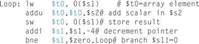
Reorder the instructions to avoid as many pipeline stalls as possible. Assume branches are predicted, so that control hazards are handled by the hardware.
Answer
The first three instructions have data dependences, and so do the last two. Figure 4.70 shows the best schedule for these instructions. Notice that just one pair of instructions has both issue slots used. It takes four clocks per loop iteration; at four clocks to execute five instructions, we get the disappointing CPI of 0.8 versus the best case of 0.5., or an IPC of 1.25 versus 2.0. Notice that in computing CPI or IPC, we do not count any nops executed as useful instructions. Doing so would improve CPI, but not performance!
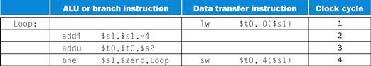
FIGURE 4.70 The scheduled code as it would look on a two-issue MIPS pipeline.
The empty slots are no-ops.
An important compiler technique to get more performance from loops is loop unrolling, where multiple copies of the loop body are made. After unrolling, there is more ILP available by overlapping instructions from different iterations.
loop unrolling
A technique to get more performance from loops that access arrays, in which multiple copies of the loop body are made and instructions from different iterations are scheduled together.
Loop Unrolling for Multiple-Issue Pipelines
Example
See how well loop unrolling and scheduling work in the example above. For simplicity assume that the loop index is a multiple of four.
Answer
To schedule the loop without any delays, it turns out that we need to make four copies of the loop body. After unrolling and eliminating the unnecessary loop overhead instructions, the loop will contain four copies each of lw, add, and sw, plus one addi and one bne. Figure 4.71 shows the unrolled and scheduled code.
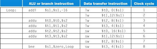
FIGURE 4.71 The unrolled and scheduled code of Figure 4.70 as it would look on a static two-issue MIPS pipeline.
The empty slots are no-ops. Since the first instruction in the loop decrements $s1 by 16, the addresses loaded are the original value of $s1, then that address minus 4, minus 8, and minus 12.
During the unrolling process, the compiler introduced additional registers ($t1, $t2, $t3). The goal of this process, called register renaming, is to eliminate dependences that are not true data dependences, but could either lead to potential hazards or prevent the compiler from flexibly scheduling the code. Consider how the unrolled code would look using only $t0. There would be repeated instances of lw $t0,0($$s1), addu $t0,$t0,$s2 followed by sw t0,4($s1), but these sequences, despite using $t0, are actually completely independent—no data values flow between one set of these instructions and the next set. This case is what is called an antidependence or name dependence, which is an ordering forced purely by the reuse of a name, rather than a real data dependence that is also called a true dependence.
register renaming
The renaming of registers by the compiler or hardware to remove antidependences.
antidependence
Also called name dependence. An ordering forced by the reuse of a name, typically a register, rather than by a true dependence that carries a value between two instructions.
Renaming the registers during the unrolling process allows the compiler to move these independent instructions subsequently so as to better schedule the code. The renaming process eliminates the name dependences, while preserving the true dependences.
Notice now that 12 of the 14 instructions in the loop execute as pairs. It takes 8 clocks for 4 loop iterations, or 2 clocks per iteration, which yields a CPI of 8/14=0.57. Loop unrolling and scheduling with dual issue gave us an improvement factor of almost 2, partly from reducing the loop control instructions and partly from dual issue execution. The cost of this performance improvement is using four temporary registers rather than one, as well as a significant increase in code size.
Dynamic Multiple-Issue Processors
Dynamic multiple-issue processors are also known as superscalar processors, or simply superscalars. In the simplest superscalar processors, instructions issue in order, and the processor decides whether zero, one, or more instructions can issue in a given clock cycle. Obviously, achieving good performance on such a processor still requires the compiler to try to schedule instructions to move dependences apart and thereby improve the instruction issue rate. Even with such compiler scheduling, there is an important difference between this simple superscalar and a VLIW processor: the code, whether scheduled or not, is guaranteed by the hardware to execute correctly. Furthermore, compiled code will always run correctly independent of the issue rate or pipeline structure of the processor. In some VLIW designs, this has not been the case, and recompilation was required when moving across different processor models; in other static issue processors, code would run correctly across different implementations, but often so poorly as to make compilation effectively required.
superscalar
An advanced pipelining technique that enables the processor to execute more than one instruction per clock cycle by selecting them during execution.
Many superscalars extend the basic framework of dynamic issue decisions to include dynamic pipeline scheduling. Dynamic pipeline scheduling chooses which instructions to execute in a given clock cycle while trying to avoid hazards and stalls. Let’s start with a simple example of avoiding a data hazard. Consider the following code sequence:
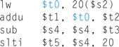
dynamic pipeline scheduling
Hardware support for reordering the order of instruction execution so as to avoid stalls.
Even though the sub instruction is ready to execute, it must wait for the lw and addu to complete first, which might take many clock cycles if memory is slow. (Chapter 5 explains cache misses, the reason that memory accesses are sometimes very slow.) Dynamic pipeline scheduling allows such hazards to be avoided either fully or partially.
Dynamic Pipeline Scheduling
Dynamic pipeline scheduling chooses which instructions to execute next, possibly reordering them to avoid stalls. In such processors, the pipeline is divided into three major units: an instruction fetch and issue unit, multiple functional units (a dozen or more in high-end designs in 2013), and a commit unit. Figure 4.72 shows the model. The first unit fetches instructions, decodes them, and sends each instruction to a corresponding functional unit for execution. Each functional unit has buffers, called reservation stations, which hold the operands and the operation. (In the next section, we will discusses an alternative to reservation stations used by many recent processors.) As soon as the buffer contains all its operands and the functional unit is ready to execute, the result is calculated. When the result is completed, it is sent to any reservation stations waiting for this particular result as well as to the commit unit, which buffers the result until it is safe to put the result into the register file or, for a store, into memory. The buffer in the commit unit, often called the reorder buffer, is also used to supply operands, in much the same way as forwarding logic does in a statically scheduled pipeline. Once a result is committed to the register file, it can be fetched directly from there, just as in a normal pipeline.
commit unit
The unit in a dynamic or out-of-order execution pipeline that decides when it is safe to release the result of an operation to programmer-visible registers and memory.
reservation station
A buffer within a functional unit that holds the operands and the operation.
reorder buffer
The buffer that holds results in a dynamically scheduled processor until it is safe to store the results to memory or a register.
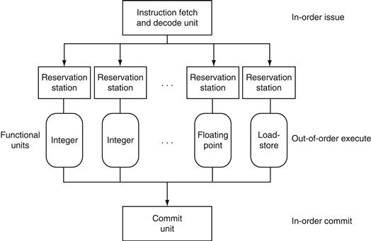
FIGURE 4.72 The three primary units of a dynamically scheduled pipeline.
The final step of updating the state is also called retirement or graduation.
The combination of buffering operands in the reservation stations and results in the reorder buffer provides a form of register renaming, just like that used by the compiler in our earlier loop-unrolling example on page 338. To see how this conceptually works, consider the following steps:
1. When an instruction issues, it is copied to a reservation station for the appropriate functional unit. Any operands that are available in the register file or reorder buffer are also immediately copied into the reservation station. The instruction is buffered in the reservation station until all the operands and the functional unit are available. For the issuing instruction, the register copy of the operand is no longer required, and if a write to that register occurred, the value could be overwritten.
2. If an operand is not in the register file or reorder buffer, it must be waiting to be produced by a functional unit. The name of the functional unit that will produce the result is tracked. When that unit eventually produces the result, it is copied directly into the waiting reservation station from the functional unit bypassing the registers.
These steps effectively use the reorder buffer and the reservation stations to implement register renaming.
Conceptually, you can think of a dynamically scheduled pipeline as analyzing the data flow structure of a program. The processor then executes the instructions in some order that preserves the data flow order of the program. This style of execution is called an out-of-order execution, since the instructions can be executed in a different order than they were fetched.
out-of-order execution
A situation in pipelined execution when an instruction blocked from executing does not cause the following instructions to wait.
To make programs behave as if they were running on a simple in-order pipeline, the instruction fetch and decode unit is required to issue instructions in order, which allows dependences to be tracked, and the commit unit is required to write results to registers and memory in program fetch order. This conservative mode is called in-order commit. Hence, if an exception occurs, the computer can point to the last instruction executed, and the only registers updated will be those written by instructions before the instruction causing the exception. Although the front end (fetch and issue) and the back end (commit) of the pipeline run in order, the functional units are free to initiate execution whenever the data they need is available. Today, all dynamically scheduled pipelines use in-order commit.
in-order commit
A commit in which the results of pipelined execution are written to the programmer visible state in the same order that instructions are fetched.
Dynamic scheduling is often extended by including hardware-based speculation, especially for branch outcomes. By predicting the direction of a branch, a dynamically scheduled processor can continue to fetch and execute instructions along the predicted path. Because the instructions are committed in order, we know whether or not the branch was correctly predicted before any instructions from the predicted path are committed. A speculative, dynamically scheduled pipeline can also support speculation on load addresses, allowing load-store reordering, and using the commit unit to avoid incorrect speculation. In the next section, we will look at the use of dynamic scheduling with speculation in the Intel Core i7 design.
Understanding Program Performance
Given that compilers can also schedule code around data dependences, you might ask why a superscalar processor would use dynamic scheduling. There are three major reasons. First, not all stalls are predictable. In particular, cache misses (see Chapter 5) in the memory hierarchy cause unpredictable stalls. Dynamic scheduling allows the processor to hide some of those stalls by continuing to execute instructions while waiting for the stall to end.

Second, if the processor speculates on branch outcomes using dynamic branch prediction, it cannot know the exact order of instructions at compile time, since it depends on the predicted and actual behavior of branches. Incorporating dynamic speculation to exploit more instruction-level parallelism (ILP) without incorporating dynamic scheduling would significantly restrict the benefits of speculation.
Third, as the pipeline latency and issue width change from one implementation to another, the best way to compile a code sequence also changes. For example, how to schedule a sequence of dependent instructions is affected by both issue width and latency. The pipeline structure affects both the number of times a loop must be unrolled to avoid stalls as well as the process of compiler-based register renaming. Dynamic scheduling allows the hardware to hide most of these details. Thus, users and software distributors do not need to worry about having multiple versions of a program for different implementations of the same instruction set. Similarly, old legacy code will get much of the benefit of a new implementation without the need for recompilation.
The BIG Picture
Both pipelining and multiple-issue execution increase peak instruction throughput and attempt to exploit instruction-level parallelism (ILP). Data and control dependences in programs, however, offer an upper limit on sustained performance because the processor must sometimes wait for a dependence to be resolved. Software-centric approaches to exploiting ILP rely on the ability of the compiler to find and reduce the effects of such dependences, while hardware-centric approaches rely on extensions to the pipeline and issue mechanisms. Speculation, performed by the compiler or the hardware, can increase the amount of ILP that can be exploited via prediction, although care must be taken since speculating incorrectly is likely to reduce performance.
Hardware/Software Interface
Modern, high-performance microprocessors are capable of issuing several instructions per clock; unfortunately, sustaining that issue rate is very difficult. For example, despite the existence of processors with four to six issues per clock, very few applications can sustain more than two instructions per clock. There are two primary reasons for this.
First, within the pipeline, the major performance bottlenecks arise from dependences that cannot be alleviated, thus reducing the parallelism among instructions and the sustained issue rate. Although little can be done about true data dependences, often the compiler or hardware does not know precisely whether a dependence exists or not, and so must conservatively assume the dependence exists. For example, code that makes use of pointers, particularly in ways that may lead to aliasing, will lead to more implied potential dependences. In contrast, the greater regularity of array accesses often allows a compiler to deduce that no dependences exist. Similarly, branches that cannot be accurately predicted whether at runtime or compile time will limit the ability to exploit ILP. Often, additional ILP is available, but the ability of the compiler or the hardware to find ILP that may be widely separated (sometimes by the execution of thousands of instructions) is limited.
Second, losses in the memory hierarchy (the topic of Chapter 5) also limit the ability to keep the pipeline full. Some memory system stalls can be hidden, but limited amounts of ILP also limit the extent to which such stalls can be hidden.
Energy Efficiency and Advanced Pipelining
The downside to the increasing exploitation of instruction-level parallelism via dynamic multiple issue and speculation is potential energy inefficiency. Each innovation was able to turn more transistors into performance, but they often did so very inefficiently. Now that we have hit the power wall, we are seeing designs with multiple processors per chip where the processors are not as deeply pipelined or as aggressively speculative as the predecessors.
The belief is that while the simpler processors are not as fast as their sophisticated brethren, they deliver better performance per joule, so that they can deliver more performance per chip when designs are constrained more by energy than they are by number of transistors.
Figure 4.73 shows the number of pipeline stages, the issue width, speculation level, clock rate, cores per chip, and power of several past and recent microprocessors. Note the drop in pipeline stages and power as companies switch to multicore designs.
Elaboration
A commit unit controls updates to the register file and memory. Some dynamically scheduled processors update the register file immediately during execution, using extra registers to implement the renaming function and preserving the older copy of a register until the instruction updating the register is no longer speculative. Other processors buffer the result, typically in a structure called a reorder buffer, and the actual update to the register file occurs later as part of the commit. Stores to memory must be buffered until commit time either in a store buffer (see Chapter 5) or in the reorder buffer. The commit unit allows the store to write to memory from the buffer when the buffer has a valid address and valid data, and when the store is no longer dependent on predicted branches.
Elaboration
Memory accesses benefit from nonblocking caches, which continue servicing cache accesses during a cache miss (see Chapter 5). Out-of-order execution processors need the cache design to allow instructions to execute during a miss.
Check Yourself
State whether the following techniques or components are associated primarily with a software-or hardware-based approach to exploiting ILP. In some cases, the answer may be both.
1. Branch prediction
2. Multiple issue
3. VLIW
4. Superscalar
5. Dynamic scheduling
6. Out-of-order execution
7. Speculation
8. Reorder buffer
9. Register renaming
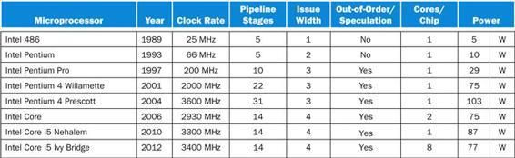
FIGURE 4.73 Record of Intel Microprocessors in terms of pipeline complexity, number of cores, and power.
The Pentium 4 pipeline stages do not include the commit stages. If we included them, the Pentium 4 pipelines would be even deeper.
4.11 Real Stuff: The ARM Cortex-A8 and Intel Core i7 Pipelines
Figure 4.74 describes the two microprocessors we examine in this section, whose targets are the two ends of the PostPC Era.
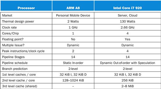
FIGURE 4.74 Specification of the ARM Cortex-A8 and the Intel Core i7 920.
The ARM Cortex-A8
The ARM Corxtex-A8 runs at 1 GHz with a 14-stage pipeline. It uses dynamic multiple issue, with two instructions per clock cycle. It is a static in-order pipeline, in that instructions issue, execute, and commit in order. The pipeline consists of three sections for instruction fetch, instruction decode, and execute. Figure 4.75 shows the overall pipeline.
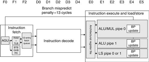
FIGURE 4.75 The A8 pipeline.
The first three stages fetch instructions into a 12-entry instruction fetch buffer. The Address Generation Unit (AGU) uses a Branch Target Buffer (BTB), Global History Buffer (GHB), and a Return Stack (RS) to predict branches to try to keep the fetch queue full. Instruction decode is five stages and instruction execution is six stages.
The first three stages fetch two instructions at a time and try to keep a 12-instruction entry prefetch buffer full. It uses a two-level branch predictor using both a 512-entry branch target buffer, a 4096-entry global history buffer, and an 8-entry return stack. When the branch prediction is wrong, it empties the pipeline, resulting in a 13-clock cycle misprediction penalty.
The five stages of the decode pipeline determine if there are dependences between a pair of instructions, which would force sequential execution, and in which pipeline of the execution stages to send the instructions.
The six stages of the instruction execution section offer one pipeline for load and store instructions and two pipelines for arithmetic operations, although only the first of the pair can handle multiplies. Either instruction from the pair can be issued to the load-store pipeline. The execution stages have full bypassing between the three pipelines.
Figure 4.76 shows the CPI of the A8 using small versions of programs derived from the SPEC2000 benchmarks. While the ideal CPI is 0.5, the best case is 1.4, the median case is 2.0, and the worst case is 5.2. For the median case, 80% of the stalls are due to the pipelining hazards and 20% are stalls due to the memory hierarchy. Pipeline stalls are caused by branch mispredictions, structural hazards, and data dependencies between pairs of instructions. Given the static pipeline of the A8, it is up to the compiler to try to avoid structural hazards and data dependences.
Elaboration
The Cortex-A8 is a configurable core that supports the ARMv7 instruction set architecture. It is delivered as an IP (Intellectual Property) core. IP cores are the dominant form of technology delivery in the embedded, personal mobile device, and related markets; billions of ARM and MIPS processors have been created from these IP cores.
Note that IP cores are different than the cores in the Intel i7 multicore computers. An IP core (which may itself be a multicore) is designed to be incorporated with other logic (hence it is the “core” of a chip), including application-specific processors (such as an encoder or decoder for video), I/O interfaces, and memory interfaces, and then fabricated to yield a processor optimized for a particular application. Although the processor core is almost identical, the resultant chips have many differences. One parameter is the size of the L2 cache, which can vary by a factor of eight.
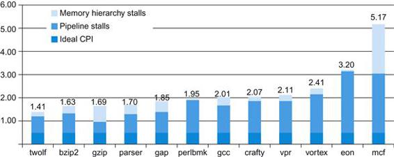
FIGURE 4.76 CPI on ARM Cortex A8 for the Minnespec benchmarks, which are small versions of the SPEC2000 benchmarks.
These benchmarks use the much smaller inputs to reduce running time by several orders of magnitude. The smaller size significantly underestimates the CPI impact of the memory hierarchy (See Chapter 5).
The Intel Core i7 920
x86 microprocessors employ sophisticated pipelining approaches, using both dynamic multiple issue and dynamic pipeline scheduling with out-of-order execution and speculation for its 14-stage pipeline. These processors, however, are still faced with the challenge of implementing the complex x86 instruction set, described in Chapter 2. Intel fetches x86 instructions and translates them into internal MIPS-like instructions, which Intel calls micro-operations. The micro-operations are then executed by a sophisticated, dynamically scheduled, speculative pipeline capable of sustaining an execution rate of up to six micro-operations per clock cycle. This section focuses on that micro-operation pipeline.
When we consider the design of sophisticated, dynamically scheduled processors, the design of the functional units, the cache and register file, instruction issue, and overall pipeline control become intermingled, making it difficult to separate the datapath from the pipeline. Because of this, many engineers and researchers have adopted the term microarchitecture to refer to the detailed internal architecture of a processor.
microarchitecture
The organization of the processor, including the major functional units, their interconnection, and control.
architectural registers
The instruction set of visible registers of a processor; for example, in MIPS, these are the 32 integer and 16 floating-point registers.
The Intel Core i7 uses a scheme for resolving antidependences and incorrect speculation that uses a reorder buffer together with register renaming. Register renaming explicitly renames the architectural registers in a processor (16 in the case of the 64-bit version of the x86 architecture) to a larger set of physical registers. The Core i7 uses register renaming to remove antidependences. Register renaming requires the processor to maintain a map between the architectural registers and the physical registers, indicating which physical register is the most current copy of an architectural register. By keeping track of the renamings that have occurred, register renaming offers another approach to recovery in the event of incorrect speculation: simply undo the mappings that have occurred since the first incorrectly speculated instruction. This will cause the state of the processor to return to the last correctly executed instruction, keeping the correct mapping between the architectural and physical registers.
Figure 4.77 shows the overall organization and pipeline of the Core i7. Below are the eight steps an x86 instruction goes through for execution.
1. Instruction fetch—The processor uses a multilevel branch target buffer to achieve a balance between speed and prediction accuracy. There is also a return address stack to speed up function return. Mispredictions cause a penalty of about 15 cycles. Using the predicted address, the instruction fetch unit fetches 16 bytes from the instruction cache.
2. The 16 bytes are placed in the predecode instruction buffer—The predecode stage transforms the 16 bytes into individual x86 instructions. This predecode is nontrivial since the length of an x86 instruction can be from 1 to 15 bytes and the predecoder must look through a number of bytes before it knows the instruction length. Individual x86 instructions are placed into the 18-entry instruction queue.
3. Micro-op decode—Individual x86 instructions are translated into micro-operations (micro-ops). Three of the decoders handle x86 instructions that translate directly into one micro-op. For x86 instructions that have more complex semantics, there is a microcode engine that is used to produce the micro-op sequence; it can produce up to four micro-ops every cycle and continues until the necessary micro-op sequence has been generated. The micro-ops are placed according to the order of the x86 instructions in the 28-entry micro-op buffer.
4. The micro-op buffer performs loop stream detection—If there is a small sequence of instructions (less than 28 instructions or 256 bytes in length) that comprises a loop, the loop stream detector will find the loop and directly issue the micro-ops from the buffer, eliminating the need for the instruction fetch and instruction decode stages to be activated.
5. Perform the basic instruction issue—Looking up the register location in the register tables, renaming the registers, allocating a reorder buffer entry, and fetching any results from the registers or reorder buffer before sending the micro-ops to the reservation stations.
6. The i7 uses a 36-entry centralized reservation station shared by six functional units. Up to six micro-ops may be dispatched to the functional units every clock cycle.
7. The individual function units execute micro-ops and then results are sent back to any waiting reservation station as well as to the register retirement unit, where they will update the register state, once it is known that the instruction is no longer speculative. The entry corresponding to the instruction in the reorder buffer is marked as complete.
8. When one or more instructions at the head of the reorder buffer have been marked as complete, the pending writes in the register retirement unit are executed, and the instructions are removed from the reorder buffer.
Elaboration
Hardware in the second and fourth steps can combine or fuse operations together to reduce the number of operations that must be performed. Macro-op fusion in the second step takes x86 instruction combinations, such as compare followed by a branch, and fuses them into a single operation. Microfusion in the fourth step combines micro-operation pairs such as load/ALU operation and ALU operation/store and issues them to a single reservation station (where they can still issue independently), thus increasing the usage of the buffer. In a study of the Intel Core architecture, which also incorporated microfusion and macrofusion, Bird et al. [2007] discovered that microfusion had little impact on performance, while macrofusion appears to have a modest positive impact on integer performance and little impact on floating-point performance.
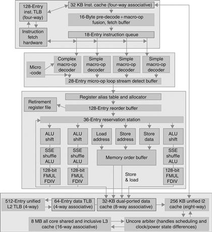
FIGURE 4.77 The Core i7 pipeline with memory components.
The total pipeline depth is 14 stages, with branch mispredictions costing 17 clock cycles. This design can buffer 48 loads and 32 stores. The six independent units can begin execution of a ready RISC operation each clock cycle.
Performance of the Intel Core i7 920
Figure 4.78 shows the CPI of the Intel Core i7 for each of the SPEC2006 benchmarks. While the ideal CPI is 0.25, the best case is 0.44, the median case is 0.79, and the worst case is 2.67.
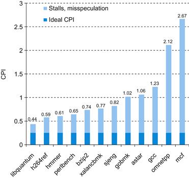
FIGURE 4.78 CPI of Intel Core i7 920 running SPEC2006 integer benchmarks.
While it is difficult to differentiate between pipeline stalls and memory stalls in a dynamic out-of-order execution pipeline, we can show the effectiveness of branch prediction and speculation. Figure 4.79shows the percentage of branches mispredicted and the percentage of the work (measured by the numbers of micro-ops dispatched into the pipeline) that does not retire (that is, their results are annulled) relative to all micro-op dispatches. The min, median, and max of branch mispredictions are 0%, 2%, and 10%. For wasted work, they are 1%, 18%, and 39%.
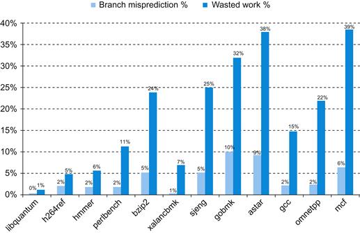
FIGURE 4.79 Percentage of branch mispredictions and wasted work due to unfruitful speculation of Intel Core i7 920 running SPEC2006 integer benchmarks.
The wasted work in some cases closely matches the branch misprediction rates, such as for gobmk and astar. In several instances, such as mcf, the wasted work seems relatively larger than the misprediction rate. This divergence is likely due to the memory behavior. With very high data cache miss rates, mcf will dispatch many instructions during an incorrect speculation as long as sufficient reservation stations are available for the stalled memory references. When a branch among the many speculated instructions is finally mispredicted, the micro-ops corresponding to all these instructions will be flushed.
Understanding Program Performance
The Intel Core i7 combines a 14-stage pipeline and aggressive multiple issue to achieve high performance. By keeping the latencies for back-to-back operations low, the impact of data dependences is reduced. What are the most serious potential performance bottlenecks for programs running on this processor? The following list includes some potential performance problems, the last three of which can apply in some form to any high-performance pipelined processor.
■ The use of x86 instructions that do not map to a few simple micro-operations
■ Branches that are difficult to predict, causing misprediction stalls and restarts when speculation fails
■ Long dependences—typically caused by long-running instructions or the memory hierarchy—that lead to stalls
■ Performance delays arising in accessing memory (see Chapter 5) that cause the processor to stall
4.12 Going Faster: Instruction-Level Parallelism and Matrix Multiply
Returning to the DGEMM example from Chapter 3, we can see the impact of instruction level parallelism by unrolling the loop so that the multiple issue, out-of-order execution processor has more instructions to work with. Figure 4.80 shows the unrolled version of Figure 3.23, which contains the C intrinsics to produce the AVX instructions.
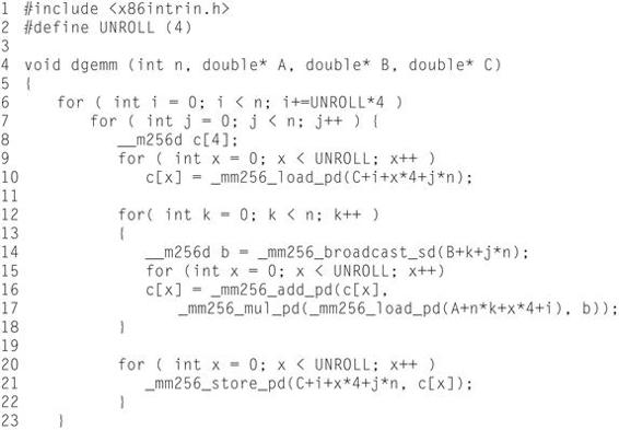
FIGURE 4.80 Optimized C version of DGEMM using C intrinsics to generate the AVX subword-parallel instructions for the x86 (Figure 3.23) and loop unrolling to create more opportunities for instruction-level parallelism.
Figure 4.81 shows the assembly language produced by the compiler for the inner loop, which unrolls the three for-loop bodies to expose instruction level parallelism.
Like the unrolling example in Figure 4.71 above, we are going to unroll the loop 4 times. (We use the constant UNROLL in the C code to control the amount of unrolling in case we want to try other values.) Rather than manually unrolling the loop in C by making 4 copies of each of the intrinsics in Figure 3.23, we can rely on the gcc compiler to do the unrolling at −O3 optimization. We surround each intrinsic with a simple for loop that 4 iterations (lines 9, 14, and 20) and replace the scalar C0 in Figure 3.23 with a 4-element array c[] (lines 8, 10, 16, and 21).
Figure 4.81 shows the assembly language output of the unrolled code. As expected, in Figure 4.81 there are 4 versions of each of the AVX instructions in Figure 3.24, with one exception. We only need 1 copy of the vbroadcastsd instruction, since we can use the four copies of the B element in register %ymm0 repeatedly throughout the loop. Thus the 5 AVX instructions in Figure 3.24 become 17 in Figure 4.81, and the 7 integer instructions appear in both, although the constants and addressing changes to account for the unrolling. Hence, despite unrolling 4 times, the number of instructions in the body of the loop only doubles: from 12 to 24.
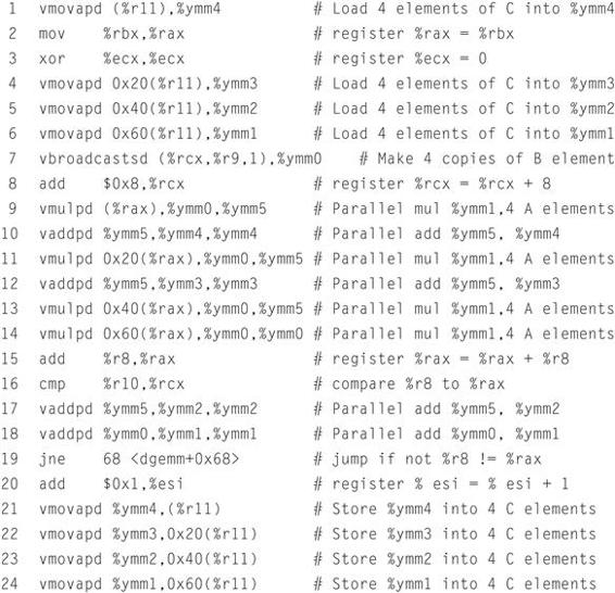
FIGURE 4.81 The x86 assembly language for the body of the nested loops generated by compiling the unrolled C code in Figure 4.80.
Figure 4.82 shows the performance increase DGEMM for 32x32 matrices in going from unoptimized to AVX and then to AVX with unrolling. Unrolling more than doubles performance, going from 6.4 GFLOPS to 14.6 GFLOPS. Optimizations for subword parallelism and instruction level parallelism result in an overall speedup of 8.8 versus the unoptimized DGEMM in Figure 3.21.
Elaboration
As mentioned in the Elaboration in Section 3.8, these results are with Turbo mode turned off. If we turn it on, like in Chapter 3 we improve all the results by the temporary increase in the clock rate of 3.3/2.6=1.27 to 2.1 GFLOPS for unoptimized DGEMM, 8.1 GFLOPS with AVX, and 18.6 GFLOPS with unrolling and AVX. As mentioned in Section 3.8, Turbo mode works particularly well in this case because it is using only a single core of an eight-core chip.
Elaboration
There are no pipeline stalls despite the reuse of register %ymm5 in lines 9 to 17 Figure 4.81 because the Intel Core i7 pipeline renames the registers.
Check Yourself
Are the following statements true or false?
1. The Intel Core i7 uses a multiple-issue pipeline to directly execute x86 instructions.
2. Both the A8 and the Core i7 use dynamic multiple issue.
3. The Core i7 microarchitecture has many more registers than x86 requires.
4. The Intel Core i7 uses less than half the pipeline stages of the earlier Intel Pentium 4 Prescott (see Figure 4.73).
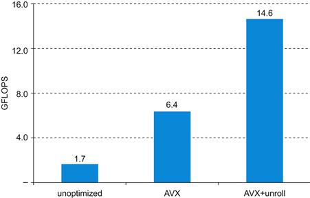
FIGURE 4.82 Performance of three versions of DGEMM for 32x32 matrices.
Subword parallelism and instruction level parallelism has led to speedup of almost a factor of 9 over the unoptimized code in Figure 3.21.
 Advanced Topic: an Introduction to Digital Design Using a Hardware Design Language to Describe and Model a Pipeline and More Pipelining Illustrations
Modern digital design is done using hardware description languages and modern computer-aided synthesis tools that can create detailed hardware designs from the descriptions using both libraries and logic synthesis. Entire books are written on such languages and their use in digital design. This section, which appears online, gives a brief introduction and shows how a hardware design language, Verilog in this case, can be used to describe the MIPS control both behaviorally and in a form suitable for hardware synthesis. It then provides a series of behavioral models in Verilog of the MIPS five-stage pipeline. The initial model ignores hazards, and additions to the model highlight the changes for forwarding, data hazards, and branch hazards.
We then provide about a dozen illustrations using the single-cycle graphical pipeline representation for readers who want to see more detail on how pipelines work for a few sequences of MIPS instructions.
4.14 Fallacies and Pitfalls
Fallacy: Pipelining is easy.
Our books testify to the subtlety of correct pipeline execution. Our advanced book had a pipeline bug in its first edition, despite its being reviewed by more than 100 people and being class-tested at 18 universities. The bug was uncovered only when someone tried to build the computer in that book. The fact that the Verilog to describe a pipeline like that in the Intel Core i7 will be many thousands of lines is an indication of the complexity. Beware!
Fallacy: Pipelining ideas can be implemented independent of technology.
When the number of transistors on-chip and the speed of transistors made a five-stage pipeline the best solution, then the delayed branch (see the first Elaboration on page 255) was a simple solution to control hazards. With longer pipelines, superscalar execution, and dynamic branch prediction, it is now redundant. In the early 1990s, dynamic pipeline scheduling took too many resources and was not required for high performance, but as transistor budgets continued to double due to Moore’s Law and logic became much faster than memory, then multiple functional units and dynamic pipelining made more sense. Today, concerns about power are leading to less aggressive designs.
Pitfall: Failure to consider instruction set design can adversely impact pipelining.
Many of the difficulties of pipelining arise because of instruction set complications. Here are some examples:
■ Widely variable instruction lengths and running times can lead to imbalance among pipeline stages and severely complicate hazard detection in a design pipelined at the instruction set level. This problem was overcome, initially in the DEC VAX 8500 in the late 1980s, using the micro-operations and micropipelined scheme that the Intel Core i7 employs today. Of course, the overhead of translation and maintaining correspondence between the micro-operations and the actual instructions remains.
■ Sophisticated addressing modes can lead to different sorts of problems. Addressing modes that update registers complicate hazard detection. Other addressing modes that require multiple memory accesses substantially complicate pipeline control and make it difficult to keep the pipeline flowing smoothly.
■ Perhaps the best example is the DEC Alpha and the DEC NVAX. In comparable technology, the newer instruction set architecture of the Alpha allowed an implementation whose performance is more than twice as fast as NVAX. In another example, Bhandarkar and Clark [1991] compared the MIPS M/2000 and the DEC VAX 8700 by counting clock cycles of the SPEC benchmarks; they concluded that although the MIPS M/2000 executes more instructions, the VAX on average executes 2.7 times as many clock cycles, so the MIPS is faster.
4.15 Concluding Remarks
Nine-tenths of wisdom consists of being wise in time.
American proverb
As we have seen in this chapter, both the datapath and control for a processor can be designed starting with the instruction set architecture and an understanding of the basic characteristics of the technology. In Section 4.3, we saw how the datapath for a MIPS processor could be constructed based on the architecture and the decision to build a single-cycle implementation. Of course, the underlying technology also affects many design decisions by dictating what components can be used in the datapath, as well as whether a single-cycle implementation even makes sense.
Pipelining improves throughput but not the inherent execution time, or instruction latency, of instructions; for some instructions, the latency is similar in length to the single-cycle approach. Multiple instruction issue adds additional datapath hardware to allow multiple instructions to begin every clock cycle, but at an increase in effective latency. Pipelining was presented as reducing the clock cycle time of the simple single-cycle datapath. Multiple instruction issue, in comparison, clearly focuses on reducing clock cycles per instruction (CPI).
instruction latency
The inherent execution time for an instruction.
Pipelining and multiple issue both attempt to exploit instruction-level parallelism. The presence of data and control dependences, which can become hazards, are the primary limitations on how much parallelism can be exploited. Scheduling and speculation via prediction, both in hardware and in software, are the primary techniques used to reduce the performance impact of dependences.
We showed that unrolling the DGEMM loop four times exposed more instructions that could take advantage of the out-of-order execution engine of the Core i7 to more than double performance.
The switch to longer pipelines, multiple instruction issue, and dynamic scheduling in the mid-1990s has helped sustain the 60% per year processor performance increase that started in the early 1980s. As mentioned in Chapter 1, these microprocessors preserved the sequential programming model, but they eventually ran into the power wall. Thus, the industry has been forced to switch to multiprocessors, which exploit parallelism at much coarser levels (the subject of Chapter 6). This trend has also caused designers to reassess the energy-performance implications of some of the inventions since the mid-1990s, resulting in a simplification of pipelines in the more recent versions of microarchitectures.
To sustain the advances in processing performance via parallel processors, Amdahl’s law suggests that another part of the system will become the bottleneck. That bottleneck is the topic of the next chapter: the memory hierarchy.
 Historical Perspective and Further Reading
This section, which appears online, discusses the history of the first pipelined processors, the earliest superscalars, and the development of out-of-order and speculative techniques, as well as important developments in the accompanying compiler technology.
4.17 Exercises
4.1 Consider the following instruction:
Instruction: AND Rd,Rs,Rt
Interpretation: Reg[Rd] = Reg[Rs] AND Reg[Rt]
4.1.1 [5] <§4.1> What are the values of control signals generated by the control in Figure 4.2 for the following instruction?
4.1.2 [5] <§4.1> Which resources (blocks) perform a useful function for this instruction?
4.1.3 [10] <§4.1> Which resources (blocks) produce outputs, but their outputs are not used for this instruction? Which resources produce no outputs for this instruction?
4.2 The basic single-cycle MIPS implementation in Figure 4.2 can only implement some instructions. New instructions can be added to an existing Instruction Set Architecture (ISA), but the decision whether or not to do that depends, among other things, on the cost and complexity the proposed addition introduces into the processor datapath and control. The first three problems in this exercise refer to the new instruction:
Instruction: LWI Rt,Rd(Rs)
Interpretation: Reg[Rt] = Mem[Reg[Rd]+Reg[Rs]]
4.2.1 [10] <§4.1> Which existing blocks (if any) can be used for this instruction?
4.2.2 [10] <§4.1> Which new functional blocks (if any) do we need for this instruction?
4.2.3 [10] <§4.1> What new signals do we need (if any) from the control unit to support this instruction?
4.3 When processor designers consider a possible improvement to the processor datapath, the decision usually depends on the cost/performance trade-off. In the following three problems, assume that we are starting with a datapath from Figure 4.2, where I-Mem, Add, Mux, ALU, Regs, D-Mem, and Control blocks have latencies of 400 ps, 100 ps, 30 ps, 120 ps, 200 ps, 350 ps, and 100 ps, respectively, and costs of 1000, 30, 10, 100, 200, 2000, and 500, respectively.
Consider the addition of a multiplier to the ALU. This addition will add 300 ps to the latency of the ALU and will add a cost of 600 to the ALU. The result will be 5% fewer instructions executed since we will no longer need to emulate the MUL instruction.
4.3.1 [10] <§4.1> What is the clock cycle time with and without this improvement?
4.3.2 [10] <§4.1> What is the speedup achieved by adding this improvement?
4.3.3 [10] <§4.1> Compare the cost/performance ratio with and without this improvement.
4.4 Problems in this exercise assume that logic blocks needed to implement a processor’s datapath have the following latencies:
![]()
4.4.1 [10] <§4.3> If the only thing we need to do in a processor is fetch consecutive instructions (Figure 4.6), what would the cycle time be?
4.4.2 [10] <§4.3> Consider a datapath similar to the one in Figure 4.11, but for a processor that only has one type of instruction: unconditional PC-relative branch. What would the cycle time be for this datapath?
4.4.3 [10] <§4.3> Repeat 4.4.2, but this time we need to support only conditional PC-relative branches.
The remaining three problems in this exercise refer to the datapath element Shift-left-2:
4.4.4 [10] <§4.3> Which kinds of instructions require this resource?
4.4.5 [20] <§4.3> For which kinds of instructions (if any) is this resource on the critical path?
4.4.6 [10] <§4.3> Assuming that we only support beq and add instructions, discuss how changes in the given latency of this resource affect the cycle time of the processor. Assume that the latencies of other resources do not change.
4.5 For the problems in this exercise, assume that there are no pipeline stalls and that the breakdown of executed instructions is as follows:
![]()
4.5.1 [10] <§4.3> In what fraction of all cycles is the data memory used?
4.5.2 [10] <§4.3> In what fraction of all cycles is the input of the sign-extend circuit needed? What is this circuit doing in cycles in which its input is not needed?
4.6 When silicon chips are fabricated, defects in materials (e.g., silicon) and manufacturing errors can result in defective circuits. A very common defect is for one wire to affect the signal in another. This is called a cross-talk fault. A special class of cross-talk faults is when a signal is connected to a wire that has a constant logical value (e.g., a power supply wire). In this case we have a stuck-at-0 or a stuck-at-1 fault, and the affected signal always has a logical value of 0 or 1, respectively. The following problems refer to bit 0 of the Write Register input on the register file in Figure 4.24.
4.6.1 [10] <§§4.3, 4.4> Let us assume that processor testing is done by filling the PC, registers, and data and instruction memories with some values (you can choose which values), letting a single instruction execute, then reading the PC, memories, and registers. These values are then examined to determine if a particular fault is present. Can you design a test (values for PC, memories, and registers) that would determine if there is a stuck-at-0 fault on this signal?
4.6.2 [10] <§§4.3, 4.4> Repeat 4.6.1 for a stuck-at-1 fault. Can you use a single test for both stuck-at-0 and stuck-at-1? If yes, explain how; if no, explain why not.
4.6.3 [60] <§§4.3, 4.4> If we know that the processor has a stuck-at-1 fault on this signal, is the processor still usable? To be usable, we must be able to convert any program that executes on a normal MIPS processor into a program that works on this processor. You can assume that there is enough free instruction memory and data memory to let you make the program longer and store additional data. Hint: the processor is usable if every instruction “broken” by this fault can be replaced with a sequence of “working” instructions that achieve the same effect.
4.6.4 [10] <§§4.3, 4.4> Repeat 4.6.1, but now the fault to test for is whether the “MemRead” control signal becomes 0 if RegDst control signal is 0, no fault otherwise.
4.6.5 [10] <§§4.3, 4.4> Repeat 4.6.4, but now the fault to test for is whether the “Jump” control signal becomes 0 if RegDst control signal is 0, no fault otherwise.
4.7 In this exercise we examine in detail how an instruction is executed in a single-cycle datapath. Problems in this exercise refer to a clock cycle in which the processor fetches the following instruction word:
10101100011000100000000000010100.
Assume that data memory is all zeros and that the processor’s registers have the following values at the beginning of the cycle in which the above instruction word is fetched:

4.7.1 [5] <§4.4> What are the outputs of the sign-extend and the jump “Shift left 2” unit (near the top of Figure 4.24) for this instruction word?
4.7.2 [10] <§4.4> What are the values of the ALU control unit’s inputs for this instruction?
4.7.3 [10] <§4.4> What is the new PC address after this instruction is executed? Highlight the path through which this value is determined.
4.7.4 [10] <§4.4> For each Mux, show the values of its data output during the execution of this instruction and these register values.
4.7.5 [10] <§4.4> For the ALU and the two add units, what are their data input values?
4.7.6 [10] <§4.4> What are the values of all inputs for the “Registers” unit?
4.8 In this exercise, we examine how pipelining affects the clock cycle time of the processor. Problems in this exercise assume that individual stages of the datapath have the following latencies:
![]()
Also, assume that instructions executed by the processor are broken down as follows:
![]()
4.8.1 [5] <§4.5> What is the clock cycle time in a pipelined and non-pipelined processor?
4.8.2 [10] <§4.5> What is the total latency of an LW instruction in a pipelined and non-pipelined processor?
4.8.3 [10] <§4.5> If we can split one stage of the pipelined datapath into two new stages, each with half the latency of the original stage, which stage would you split and what is the new clock cycle time of the processor?
4.8.4 [10] <§4.5> Assuming there are no stalls or hazards, what is the utilization of the data memory?
4.8.5 [10] <§4.5> Assuming there are no stalls or hazards, what is the utilization of the write-register port of the “Registers” unit?
4.8.6 [30] <§4.5> Instead of a single-cycle organization, we can use a multi-cycle organization where each instruction takes multiple cycles but one instruction finishes before another is fetched. In this organization, an instruction only goes through stages it actually needs (e.g., ST only takes 4 cycles because it does not need the WB stage). Compare clock cycle times and execution times with single-cycle, multi-cycle, and pipelined organization.
4.9 In this exercise, we examine how data dependences affect execution in the basic 5-stage pipeline described in Section 4.5. Problems in this exercise refer to the following sequence of instructions:
or r1, r2, r3
or r2, r1, r4
or r1, r1, r2
Also, assume the following cycle times for each of the options related to forwarding:
|
Without Forwarding |
With Full Forwarding |
With ALU-ALU Forwarding Only |
|
250 ps |
300 ps |
290 ps |
4.9.1 [10] <§4.5> Indicate dependences and their type.
4.9.2 [10] <§4.5> Assume there is no forwarding in this pipelined processor. Indicate hazards and add nop instructions to eliminate them.
4.9.3 [10] <§4.5> Assume there is full forwarding. Indicate hazards and add nop instructions to eliminate them.
4.9.4 [10] <§4.5> What is the total execution time of this instruction sequence without forwarding and with full forwarding? What is the speedup achieved by adding full forwarding to a pipeline that had no forwarding?
4.9.5 [10] <§4.5> Add nop instructions to this code to eliminate hazards if there is ALU-ALU forwarding only (no forwarding from the MEM to the EX stage).
4.9.6 [10] <§4.5> What is the total execution time of this instruction sequence with only ALU-ALU forwarding? What is the speedup over a no-forwarding pipeline?
4.10 In this exercise, we examine how resource hazards, control hazards, and Instruction Set Architecture (ISA) design can affect pipelined execution. Problems in this exercise refer to the following fragment of MIPS code:
sw r16, 12(r6)
lw r16, 8(r6)
beq r5, r4, Label # Assume r5!=r4
add r5, r1, r4
slt r5, r15, r4
Assume that individual pipeline stages have the following latencies:
![]()
4.10.1 [10] <§4.5> For this problem, assume that all branches are perfectly predicted (this eliminates all control hazards) and that no delay slots are used. If we only have one memory (for both instructions and data), there is a structural hazard every time we need to fetch an instruction in the same cycle in which another instruction accesses data. To guarantee forward progress, this hazard must always be resolved in favor of the instruction that accesses data. What is the total execution time of this instruction sequence in the 5-stage pipeline that only has one memory? We have seen that data hazards can be eliminated by adding nops to the code. Can you do the same with this structural hazard? Why?
4.10.2 [20] <§4.5> For this problem, assume that all branches are perfectly predicted (this eliminates all control hazards) and that no delay slots are used. If we change load/store instructions to use a register (without an offset) as the address, these instructions no longer need to use the ALU. As a result, MEM and EX stages can be overlapped and the pipeline has only 4 stages. Change this code to accommodate this changed ISA. Assuming this change does not affect clock cycle time, what speedup is achieved in this instruction sequence?
4.10.3 [10] <§4.5> Assuming stall-on-branch and no delay slots, what speedup is achieved on this code if branch outcomes are determined in the ID stage, relative to the execution where branch outcomes are determined in the EX stage?
4.10.4 [10] <§4.5> Given these pipeline stage latencies, repeat the speedup calculation from 4.10.2, but take into account the (possible) change in clock cycle time. When EX and MEM are done in a single stage, most of their work can be done in parallel. As a result, the resulting EX/MEM stage has a latency that is the larger of the original two, plus 20 ps needed for the work that could not be done in parallel.
4.10.5 [10] <§4.5> Given these pipeline stage latencies, repeat the speedup calculation from 4.10.3, taking into account the (possible) change in clock cycle time. Assume that the latency ID stage increases by 50% and the latency of the EX stage decreases by 10 ps when branch outcome resolution is moved from EX to ID.
4.10.6 [10] <§4.5> Assuming stall-on-branch and no delay slots, what is the new clock cycle time and execution time of this instruction sequence if beq address computation is moved to the MEM stage? What is the speedup from this change? Assume that the latency of the EX stage is reduced by 20 ps and the latency of the MEM stage is unchanged when branch outcome resolution is moved from EX to MEM.
4.11 Consider the following loop.
loop:lw r1, 0(r1)
and r1, r1, r2
lw r1, 0(r1)
lw r1, 0(r1)
beq r1, r0, loop
Assume that perfect branch prediction is used (no stalls due to control hazards), that there are no delay slots, and that the pipeline has full forwarding support. Also assume that many iterations of this loop are executed before the loop exits.
4.11.1 [10] <§4.6> Show a pipeline execution diagram for the third iteration of this loop, from the cycle in which we fetch the first instruction of that iteration up to (but not including) the cycle in which we can fetch the first instruction of the next iteration. Show all instructions that are in the pipeline during these cycles (not just those from the third iteration).
4.11.2 [10] <§4.6> How often (as a percentage of all cycles) do we have a cycle in which all five pipeline stages are doing useful work?
4.12 This exercise is intended to help you understand the cost/complexity/performance trade-offs of forwarding in a pipelined processor. Problems in this exercise refer to pipelined datapaths from Figure 4.45. These problems assume that, of all the instructions executed in a processor, the following fraction of these instructions have a particular type of RAW data dependence. The type of RAW data dependence is identified by the stage that produces the result (EX or MEM) and the instruction that consumes the result (1st instruction that follows the one that produces the result, 2nd instruction that follows, or both). We assume that the register write is done in the first half of the clock cycle and that register reads are done in the second half of the cycle, so “EX to 3rd” and “MEM to 3rd” dependences are not counted because they cannot result in data hazards. Also, assume that the CPI of the processor is 1 if there are no data hazards.

Assume the following latencies for individual pipeline stages. For the EX stage, latencies are given separately for a processor without forwarding and for a processor with different kinds of forwarding.

4.12.1 [10] <§4.7> If we use no forwarding, what fraction of cycles are we stalling due to data hazards?
4.12.2 [5] <§4.7> If we use full forwarding (forward all results that can be forwarded), what fraction of cycles are we staling due to data hazards?
4.12.3 [10] <§4.7> Let us assume that we cannot afford to have three-input Muxes that are needed for full forwarding. We have to decide if it is better to forward only from the EX/MEM pipeline register (next-cycle forwarding) or only from the MEM/WB pipeline register (two-cycle forwarding). Which of the two options results in fewer data stall cycles?
4.12.4 [10] <§4.7> For the given hazard probabilities and pipeline stage latencies, what is the speedup achieved by adding full forwarding to a pipeline that had no forwarding?
4.12.5 [10] <§4.7> What would be the additional speedup (relative to a processor with forwarding) if we added time-travel forwarding that eliminates all data hazards? Assume that the yet-to-be-invented time-travel circuitry adds 100 ps to the latency of the full-forwarding EX stage.
4.12.6 [20] <§4.7> Repeat 4.12.3 but this time determine which of the two options results in shorter time per instruction.
4.13 This exercise is intended to help you understand the relationship between forwarding, hazard detection, and ISA design. Problems in this exercise refer to the following sequence of instructions, and assume that it is executed on a 5-stage pipelined datapath:
add r5, r2, r1
lw r3, 4(r5)
lw r2, 0(r2)
or r3, r5, r3
sw r3, 0(r5)
4.13.1 [5] <§4.7> If there is no forwarding or hazard detection, insert nops to ensure correct execution.
4.13.2 [10] <§4.7> Repeat 4.13.1 but now use nops only when a hazard cannot be avoided by changing or rearranging these instructions. You can assume register R7 can be used to hold temporary values in your modified code.
4.13.3 [10] <§4.7> If the processor has forwarding, but we forgot to implement the hazard detection unit, what happens when this code executes?
4.13.4 [20] <§4.7> If there is forwarding, for the first five cycles during the execution of this code, specify which signals are asserted in each cycle by hazard detection and forwarding units in Figure 4.60.
4.13.5 [10] <§4.7> If there is no forwarding, what new inputs and output signals do we need for the hazard detection unit in Figure 4.60? Using this instruction sequence as an example, explain why each signal is needed.
4.13.6 [20] <§4.7> For the new hazard detection unit from part e, specify which output signals it asserts in each of the first five cycles during the execution of this code.
4.14 This exercise is intended to help you understand the relationship between delay slots, control hazards, and branch execution in a pipelined processor. In this exercise, we assume that the following MIPS code is executed on a pipelined processor with a 5-stage pipeline, full forwarding, and a predict-taken branch predictor:
lw r2, 0(r1)
label1: beq r2, r0, label2 # not taken once, then taken
lw r3, 0(r2)
beq r3, r0, label1 # taken
add r1, r3, r1
label2: sw r1, 0(r2)
4.14.1 [10] <§4.8> Draw the pipeline execution diagram for this code, assuming there are no delay slots and that branches execute in the EX stage.
4.14.2 [10] <§4.8> Repeat part a, but assume that delay slots are used. In the given code, the instruction that follows the branch is now the delay slot instruction for that branch.
4.14.3 [20] <§4.8> One way to move the branch resolution one stage earlier is to not need an ALU operation in conditional branches. The branch instructions would be “bez rd,label” and “bnez rd, label”, and it would branch if the register has and does not have a zero value, respectively. Change this code to use these branch instructions instead of beq. You can assume that register R8 is available for you to use as a temporary register, and that an seq (set if equal) R-type instruction can be used.
Section 4.8 describes how the severity of control hazards can be reduced by moving branch execution into the ID stage. This approach involves a dedicated comparator in the ID stage, as shown in Figure 4.62. However, this approach potentially adds to the latency of the ID stage, and requires additional forwarding logic and hazard detection.
4.14.4 [10] <§4.8> Using the first branch instruction in the given code as an example, describe the hazard detection logic needed to support branch execution in the ID stage as in Figure 4.62. Which type of hazard is this new logic supposed to detect?
4.14.5 [10] <§4.8> For the given code, what is the speedup achieved by moving branch execution into the ID stage? Explain your answer. In your speedup calculation, assume that the additional comparison in the ID stage does not affect clock cycle time.
4.14.6 [10] <§4.8> Using the first branch instruction in the given code as an example, describe the forwarding support that must be added to support branch execution in the ID stage. Compare the complexity of this new forwarding unit to the complexity of the existing forwarding unit in Figure 4.62.
4.15 The importance of having a good branch predictor depends on how often conditional branches are executed. Together with branch predictor accuracy, this will determine how much time is spent stalling due to mispredicted branches. In this exercise, assume that the breakdown of dynamic instructions into various instruction categories is as follows:
![]()
Also, assume the following branch predictor accuracies:
|
Always-Taken |
Always-Not-Taken |
2-Bit |
|
45% |
55% |
85% |
4.15.1 [10] <§4.8> Stall cycles due to mispredicted branches increase the CPI. What is the extra CPI due to mispredicted branches with the always-taken predictor? Assume that branch outcomes are determined in the EX stage, that there are no data hazards, and that no delay slots are used.
4.15.2 [10] <§4.8> Repeat 4.15.1 for the “always-not-taken” predictor.
4.15.3 [10] <§4.8> Repeat 4.15.1 for for the 2-bit predictor.
4.15.4 [10] <§4.8> With the 2-bit predictor, what speedup would be achieved if we could convert half of the branch instructions in a way that replaces a branch instruction with an ALU instruction? Assume that correctly and incorrectly predicted instructions have the same chance of being replaced.
4.15.5 [10] <§4.8> With the 2-bit predictor, what speedup would be achieved if we could convert half of the branch instructions in a way that replaced each branch instruction with two ALU instructions? Assume that correctly and incorrectly predicted instructions have the same chance of being replaced.
4.15.6 [10] <§4.8> Some branch instructions are much more predictable than others. If we know that 80% of all executed branch instructions are easy-to-predict loop-back branches that are always predicted correctly, what is the accuracy of the 2-bit predictor on the remaining 20% of the branch instructions?
4.16 This exercise examines the accuracy of various branch predictors for the following repeating pattern (e.g., in a loop) of branch outcomes: T, NT, T, T, NT
4.16.1 [5] <§4.8> What is the accuracy of always-taken and always-not-taken predictors for this sequence of branch outcomes?
4.16.2 [5] <§4.8> What is the accuracy of the two-bit predictor for the first 4 branches in this pattern, assuming that the predictor starts off in the bottom left state from Figure 4.63 (predict not taken)?
4.16.3 [10] <§4.8> What is the accuracy of the two-bit predictor if this pattern is repeated forever?
4.16.4 [30] <§4.8> Design a predictor that would achieve a perfect accuracy if this pattern is repeated forever. You predictor should be a sequential circuit with one output that provides a prediction (1 for taken, 0 for not taken) and no inputs other than the clock and the control signal that indicates that the instruction is a conditional branch.
4.16.5 [10] <§4.8> What is the accuracy of your predictor from 4.16.4 if it is given a repeating pattern that is the exact opposite of this one?
4.16.6 [20] <§4.8> Repeat 4.16.4, but now your predictor should be able to eventually (after a warm-up period during which it can make wrong predictions) start perfectly predicting both this pattern and its opposite. Your predictor should have an input that tells it what the real outcome was. Hint: this input lets your predictor determine which of the two repeating patterns it is given.
4.17 This exercise explores how exception handling affects pipeline design. The first three problems in this exercise refer to the following two instructions:
|
Instruction 1 |
Instruction 2 |
|
BNE R1, R2, Label |
LW R1, 0(R1) |
4.17.1 [5] <§4.9> Which exceptions can each of these instructions trigger? For each of these exceptions, specify the pipeline stage in which it is detected.
4.17.2 [10] <§4.9> If there is a separate handler address for each exception, show how the pipeline organization must be changed to be able to handle this exception. You can assume that the addresses of these handlers are known when the processor is designed.
4.17.3 [10] <§4.9> If the second instruction is fetched right after the first instruction, describe what happens in the pipeline when the first instruction causes the first exception you listed in 4.17.1. Show the pipeline execution diagram from the time the first instruction is fetched until the time the first instruction of the exception handler is completed.
4.17.4 [20] <§4.9> In vectored exception handling, the table of exception handler addresses is in data memory at a known (fixed) address. Change the pipeline to implement this exception handling mechanism. Repeat 4.17.3 using this modified pipeline and vectored exception handling.
4.17.5 [15] <§4.9> We want to emulate vectored exception handling (described in 4.17.4) on a machine that has only one fixed handler address. Write the code that should be at that fixed address. Hint: this code should identify the exception, get the right address from the exception vector table, and transfer execution to that handler.
4.18 In this exercise we compare the performance of 1-issue and 2-issue processors, taking into account program transformations that can be made to optimize for 2-issue execution. Problems in this exercise refer to the following loop (written in C):
for(i=0;i!=j;i+=2)
b[i]=a[i]–a[i+1];
When writing MIPS code, assume that variables are kept in registers as follows, and that all registers except those indicated as Free are used to keep various variables, so they cannot be used for anything else.
![]()
4.18.1 [10] <§4.10> Translate this C code into MIPS instructions. Your translation should be direct, without rearranging instructions to achieve better performance.
4.18.2 [10] <§4.10> If the loop exits after executing only two iterations, draw a pipeline diagram for your MIPS code from part a executed on a 2-issue processor shown in Figure 4.69. Assume the processor has perfect branch prediction and can fetch any two instructions (not just consecutive instructions) in the same cycle.
4.18.3 [10] <§4.10> Rearrange your code from part a to achieve better performance on a 2-issue statically scheduled processor from Figure 4.69.
4.18.4 [10] <§4.10> Repeat 4.18.2, but this time use your MIPS code from 4.18.3.
4.18.5 [10] <§4.10> What is the speedup of going from a 1-issue processor to a 2-issue processor from Figure 4.69? Use your code from 4.18.1 for both 1-issue and 2-issue, and assume that 1,000,000 iterations of the loop are executed. As in 4.18.2, assume that the processor has perfect branch predictions, and that a 2-issue processor can fetch any two instructions in the same cycle.
4.18.6 [10] <§4.10> Repeat 4.18.5, but this time assume that in the 2-issue processor one of the instructions to be executed in a cycle can be of any kind, and the other must be a non-memory instruction.
4.19 This exercise explores energy efficiency and its relationship with performance. Problems in this exercise assume the following energy consumption for activity in Instruction memory, Registers, and Data memory. You can assume that the other components of the datapath spend a negligible amount of energy.
![]()
Assume that components in the datapath have the following latencies. You can assume that the other components of the datapath have negligible latencies.
![]()
4.19.1 [10] <§§§4.3, 4.6, 4.14> How much energy is spent to execute an ADD instruction in a single-cycle design and in the 5-stage pipelined design?
4.19.2 [10] <§§4.6, 4.14> What is the worst-case MIPS instruction in terms of energy consumption, and what is the energy spent to execute it?
4.19.3 [10] <§§4.6, 4.14> If energy reduction is paramount, how would you change the pipelined design? What is the percentage reduction in the energy spent by an LW instruction after this change?
4.19.4 [10] <§§4.6, 4.14> What is the performance impact of your changes from 4.19.3?
4.19.5 [10] <§§4.6, 4.14> We can eliminate the MemRead control signal and have the data memory be read in every cycle, i.e., we can permanently have MemRead=1. Explain why the processor still functions correctly after this change. What is the effect of this change on clock frequency and energy consumption?
4.19.6 [10] <§§4.6, 4.14> If an idle unit spends 10% of the power it would spend if it were active, what is the energy spent by the instruction memory in each cycle? What percentage of the overall energy spent by the instruction memory does this idle energy represent?
All materials on the site are licensed Creative Commons Attribution-Sharealike 3.0 Unported CC BY-SA 3.0 & GNU Free Documentation License (GFDL)
If you are the copyright holder of any material contained on our site and intend to remove it, please contact our site administrator for approval.
© 2016-2026 All site design rights belong to S.Y.A.