Computer Organization and Design (2016)
APPENDIX B
The Basics of Logic Design
Abstract
This appendix provides a brief discussion of the basics of logic design. It begins with an introduction to the basic building blocks of logic, gates. It then shows how to use these building blocks to construct simple combinational logic systems. It covers the design an ALU for the MIPS processor, shows how to make a fast adder, and includes a short introduction to the topic of clocking. Memory elements are also covered, as well as the design and use of finite-state machines. The chapter concludes with an explanation of the basics of how edge-triggered clocking works, an introduction to another clocking scheme, and a brief description of the problem of synchronizing asynchronous inputs.
Keywords
gates, truth tables, logic equations, combinational logic, hardware description language, HDL, arithmetic logic unit, ALU, carry lookahead, clock, flip-flop, latch, register, SRAM, DRAM, finite-state machine, timing, field programmable device, FPGA
I always loved that word, Boolean.
Claude Shannon, IEEE Spectrum, April 1992 (Shannon’s master’s thesis showed that the algebra invented by George Boole in the 1800s could represent the workings of electrical switches.)
B.1 Introduction
B.2 Gates, Truth Tables, and Logic Equations
B.3 Combinational Logic
B.4 Using a Hardware Description Language
B.5 Constructing a Basic Arithmetic Logic Unit
B.6 Faster Addition: Carry Lookahead
B.7 Clocks
B.8 Memory Elements: Flip-Flops, Latches, and Registers
B.9 Memory Elements: SRAMs and DRAMs
B.10 Finite-State Machines
B.11 Timing Methodologies
B.12 Field Programmable Devices
B.13 Concluding Remarks
B.14 Exercises
B.1 Introduction
This appendix provides a brief discussion of the basics of logic design. It does not replace a course in logic design, nor will it enable you to design significant working logic systems. If you have little or no exposure to logic design, however, this appendix will provide sufficient background to understand all the material in this book. In addition, if you are looking to understand some of the motivation behind how computers are implemented, this material will serve as a useful introduction. If your curiosity is aroused but not sated by this appendix, the references at the end provide several additional sources of information.
Section B.2 introduces the basic building blocks of logic, namely, gates. Section B.3 uses these building blocks to construct simple combinational logic systems, which contain no memory. If you have had some exposure to logic or digital systems, you will probably be familiar with the material in these first two sections. Section B.5 shows how to use the concepts of Sections B.2 and B.3 to design an ALU for the MIPS processor. Section B.6 shows how to make a fast adder, and may be safely skipped if you are not interested in this topic. Section B.7 is a short introduction to the topic of clocking, which is necessary to discuss how memory elements work. Section B.8 introduces memory elements, and Section B.9 extends it to focus on random access memories; it describes both the characteristics that are important to understanding how they are used in Chapter 4, and the background that motivates many of the aspects of memory hierarchy design in Chapter 5. Section B.10 describes the design and use of finite-state machines, which are sequential logic blocks. If you intend to read Appendix D, you should thoroughly understand the material in Sections B.2 through B.10. If you intend to read only the material on control in Chapter 4, you can skim the appendices; however, you should have some familiarity with all the material except Section B.11. Section B.11 is intended for those who want a deeper understanding of clocking methodologies and timing. It explains the basics of how edge-triggered clocking works, introduces another clocking scheme, and briefly describes the problem of synchronizing asynchronous inputs.
Throughout this appendix, where it is appropriate, we also include segments to demonstrate how logic can be represented in Verilog, which we introduce in Section B.4. A more extensive and complete Verilog tutorial appears elsewhere on the CD.
B.2 Gates, Truth Tables, and Logic Equations
The electronics inside a modern computer are digital. Digital electronics operate with only two voltage levels of interest: a high voltage and a low voltage. All other voltage values are temporary and occur while transitioning between the values. (As we discuss later in this section, a possible pitfall in digital design is sampling a signal when it not clearly either high or low.) The fact that computers are digital is also a key reason they use binary numbers, since a binary system matches the underlying abstraction inherent in the electronics. In various logic families, the values and relationships between the two voltage values differ. Thus, rather than refer to the voltage levels, we talk about signals that are (logically) true, or 1, or are asserted; or signals that are (logically) false, or 0, or are deasserted. The values 0 and 1 are called complements or inverses of one another.
asserted signal
A signal that is (logically) true, or 1.
deasserted signal
A signal that is (logically) false, or 0.
Logic blocks are categorized as one of two types, depending on whether they contain memory. Blocks without memory are called combinational; the output of a combinational block depends only on the current input. In blocks with memory, the outputs can depend on both the inputs and the value stored in memory, which is called the state of the logic block. In this section and the next, we will focus only on combinational logic. After introducing different memory elements in Section B.8, we will describe how sequential logic, which is logic including state, is designed.
combinational logic
A logic system whose blocks do not contain memory and hence compute the same output given the same input.
sequential logic
A group of logic elements that contain memory and hence whose value depends on the inputs as well as the current contents of the memory.
Truth Tables
Because a combinational logic block contains no memory, it can be completely specified by defining the values of the outputs for each possible set of input values. Such a description is normally given as a truth table. For a logic block with n inputs, there are 2n entries in the truth table, since there are that many possible combinations of input values. Each entry specifies the value of all the outputs for that particular input combination.
Truth Tables
Example
Consider a logic function with three inputs, A, B, and C, and three outputs, D, E, and F. The function is defined as follows: D is true if at least one input is true, E is true if exactly two inputs are true, and F is true only if all three inputs are true. Show the truth table for this function.
Answer
The truth table will contain 23 = 8 entries. Here it is:
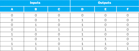
Truth tables can completely describe any combinational logic function; however, they grow in size quickly and may not be easy to understand. Sometimes we want to construct a logic function that will be 0 for many input combinations, and we use a shorthand of specifying only the truth table entries for the nonzero outputs. This approach is used in Chapter 4 and ![]() Appendix D.
Appendix D.
Boolean Algebra
Another approach is to express the logic function with logic equations. This is done with the use of Boolean algebra (named after Boole, a 19th-century mathematician). In Boolean algebra, all the variables have the values 0 or 1 and, in typical formulations, there are three operators:
■ The OR operator is written as +, as in A + B. The result of an OR operator is 1 if either of the variables is 1. The OR operation is also called a logical sum, since its result is 1 if either operand is 1.
■ The AND operator is written as ·, as in A · B. The result of an AND opera tor is 1 only if both inputs are 1. The AND operator is also called logical product, since its result is 1 only if both operands are 1.
■ The unary operator NOT is written as ![]() . The result of a NOT operator is 1 only if the input is 0. Applying the operator NOT to a logical value results in an inversion or negation of the value (i.e., if the input is 0 the output is 1, and vice versa).
. The result of a NOT operator is 1 only if the input is 0. Applying the operator NOT to a logical value results in an inversion or negation of the value (i.e., if the input is 0 the output is 1, and vice versa).
There are several laws of Boolean algebra that are helpful in manipulating logic equations.
■ Identity law: A + 0 = A and A · 1 = A.
■ Zero and One laws: A + 1 = 1 and A · 0 = 0.
■ Inverse laws: ![]() and
and ![]() .
.
■ Commutative laws: A + B = B + A and A · B = B · A.
■ Associative laws: A + (B + C) = (A + B) + C and A · (B · C) = (A · B) · C.
■ Distributive laws: A · (B + C) = (A · B) + (A · C) and A + (B · C) = (A + B) · (A + C).
In addition, there are two other useful theorems, called DeMorgan’s laws, that are discussed in more depth in the exercises.
Any set of logic functions can be written as a series of equations with an output on the left-hand side of each equation and a formula consisting of variables and the three operators above on the right-hand side.
Logic Equations
Example
Show the logic equations for the logic functions, D, E, and F, described in the previous example.
Answer
Here’s the equation for D:
![]()
F is equally simple:
![]()
E is a little tricky. Think of it in two parts: what must be true for E to be true (two of the three inputs must be true), and what cannot be true (all three cannot be true). Thus we can write E as
![]()
We can also derive E by realizing that E is true only if exactly two of the inputs are true. Then we can write E as an OR of the three possible terms that have two true inputs and one false input:
![]()
Proving that these two expressions are equivalent is explored in the exercises.
In Verilog, we describe combinational logic whenever possible using the assign statement, which is described beginning on page B-23. We can write a definition for E using the Verilog exclusive-OR operator as assign E = (A ^ B ^ C) (A + B + C) (A B C), which is yet another way to describe this function. D and F have even simpler representations, which are just like the corresponding C code: D = A | B | C and F = A & B & C.
Gates
Logic blocks are built from gates that implement basic logic functions. For example, an AND gate implements the AND function, and an OR gate implements the OR function. Since both AND and OR are commutative and associative, an AND or an OR gate can have multiple inputs, with the output equal to the AND or OR of all the inputs. The logical function NOT is implemented with an inverter that always has a single input. The standard representation of these three logic building blocks is shown in Figure B.2.1.
gate
A device that implements basic logic functions, such as AND or OR.
![]()
FIGURE B.2.1 Standard drawing for an AND gate, OR gate, and an inverter, shown from left to right.
The signals to the left of each symbol are the inputs, while the output appears on the right. The AND and OR gates both have two inputs. Inverters have a single input.
Rather than draw inverters explicitly, a common practice is to add “bubbles” to the inputs or outputs of a gate to cause the logic value on that input line or output line to be inverted. For example, Figure B.2.2shows the logic diagram for the function ![]() , using explicit inverters on the left and bubbled inputs and outputs on the right.
, using explicit inverters on the left and bubbled inputs and outputs on the right.
![]()
FIGURE B.2.2 Logic gate implementation of ![]() using explicit inverts on the left and bubbled inputs and outputs on the right.
using explicit inverts on the left and bubbled inputs and outputs on the right.
This logic function can be simplified to ![]() or in Verilog, A & ∼ B.
or in Verilog, A & ∼ B.
Any logical function can be constructed using AND gates, OR gates, and inversion; several of the exercises give you the opportunity to try implementing some common logic functions with gates. In the next section, we’ll see how an implementation of any logic function can be constructed using this knowledge.
In fact, all logic functions can be constructed with only a single gate type, if that gate is inverting. The two common inverting gates are called NOR and NAND and correspond to inverted OR and AND gates, respectively. NOR and NAND gates are called universal, since any logic function can be built using this one gate type. The exercises explore this concept further.
NOR gate
An inverted OR gate.
NAND gate
An inverted AND gate.
Check Yourself
Are the following two logical expressions equivalent? If not, find a setting of the variables to show they are not:
■ ![]()
■ ![]()
B.3 Combinational Logic
In this section, we look at a couple of larger logic building blocks that we use heavily, and we discuss the design of structured logic that can be automatically implemented from a logic equation or truth table by a translation program. Last, we discuss the notion of an array of logic blocks.
Decoders
One logic block that we will use in building larger components is a decoder. The most common type of decoder has an n-bit input and 2n outputs, where only one output is asserted for each input combination. This decoder translates the n-bit input into a signal that corresponds to the binary value of the n-bit input. The outputs are thus usually numbered, say, Out0, Out1, …, Out2n − 1. If the value of the input is i, then Outi will be true and all other outputs will be false. Figure B.3.1 shows a 3-bit decoder and the truth table. This decoder is called a 3-to-8 decoder since there are 3 inputs and 8 (23) outputs. There is also a logic element called an encoder that performs the inverse function of a decoder, taking 2n inputs and producing an n-bit output.
decoder
A logic block that has an n-bit input and 2n out puts, where only one output is asserted for each input combination.

FIGURE B.3.1 A 3-bit decoder has 3 inputs, called 12, 11, and 10, and 23 = 8 outputs, called Out0 to Out7.
Only the output corresponding to the binary value of the input is true, as shown in the truth table. The label 3 on the input to the decoder says that the input signal is 3 bits wide.
Multiplexors
One basic logic function that we use quite often in Chapter 4 is the multiplexor. A multiplexor might more properly be called a selector, since its output is one of the inputs that is selected by a control. Consider the two-input multiplexor. The left side of Figure B.3.2 shows this multiplexor has three inputs: two data val ues and a selector ( or control) value. The selector value determines which of the inputs becomes the output. We can represent the logic function computed by a two-input multiplexor, shown in gate form on the right side of Figure B.3.2, as ![]() .
.
selector value
Also called control value. The control signal that is used to select one of the input values of a multiplexor as the output of the multiplexor.
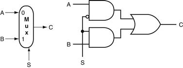
FIGURE B.3.2 A two-input multiplexor on the left and its implementation with gates on the right.
The multiplexor has two data inputs (A and B), which are labeled 0 and 1, and one selector input (S), as well as an output C. Implementing multiplexors in Verilog requires a little more work, especially when they are wider than two inputs. We show how to do this beginning on page B-23.
Multiplexors can be created with an arbitrary number of data inputs. When there are only two inputs, the selector is a single signal that selects one of the inputs if it is true (1) and the other if it is false (0). If there are n data inputs, there will need to be ![]() selector inputs. In this case, the multiplexor basically consists of three parts:
selector inputs. In this case, the multiplexor basically consists of three parts:
1. A decoder that generates n signals, each indicating a different input value
2. An array of n AND gates, each combining one of the inputs with a signal from the decoder
3. A single large OR gate that incorporates the outputs of the AND gates
To associate the inputs with selector values, we often label the data inputs numerically (i.e., 0, 1, 2, 3, …, n − 1) and interpret the data selector inputs as a binary number. Sometimes, we make use of a multiplexor with undecoded selector signals.
Multiplexors are easily represented combinationally in Verilog by using if expressions. For larger multiplexors, case statements are more convenient, but care must be taken to synthesize combinational logic.
Two-Level Logic and PLAs
As pointed out in the previous section, any logic function can be implemented with only AND, OR, and NOT functions. In fact, a much stronger result is true. Any logic function can be written in a canonical form, where every input is either a true or complemented variable and there are only two levels of gates—one being AND and the other OR—with a possible inversion on the final output. Such a representation is called a two-level representation, and there are two forms, called sum of products and product of sums. A sum-of-products representation is a logical sum (OR) of products (terms using the AND operator); a product of sums is just the opposite. In our earlier example, we had two equations for the output E:
![]()
and
![]()
sum of products
A form of logical representation that employs a logical sum (OR) of products (terms joined using the AND operator).
This second equation is in a sum-of-products form: it has two levels of logic and the only inversions are on individual variables. The first equation has three levels of logic.
Elaboration
We can also write E as a product of sums:
![]()
To derive this form, you need to use DeMorgan’s theorems, which are discussed in the exercises.
In this text, we use the sum-of-products form. It is easy to see that any logic function can be represented as a sum of products by constructing such a representation from the truth table for the function. Each truth table entry for which the function is true corresponds to a product term. The product term consists of a logical product of all the inputs or the complements of the inputs, depending on whether the entry in the truth table has a 0 or 1 corresponding to this variable. The logic function is the logical sum of the product terms where the function is true. This is more easily seen with an example.
Sum of Products
Example
Show the sum-of-products representation for the following truth table for D.
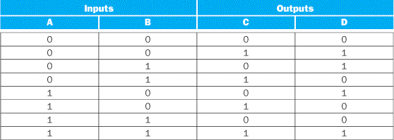
Answer
There are four product terms, since the function is true (1) for four different input combinations. These are:

Thus, we can write the function for D as the sum of these terms:
![]()
Note that only those truth table entries for which the function is true generate terms in the equation.
We can use this relationship between a truth table and a two-level representation to generate a gate-level implementation of any set of logic functions. A set of logic functions corresponds to a truth table with multiple output columns, as we saw in the example on page B-5. Each output column represents a different logic function, which may be directly constructed from the truth table.
The sum-of-products representation corresponds to a common structured-logic implementation called a programmable logic array (PLA). A PLA has a set of inputs and corresponding input complements (which can be implemented with a set of inverters), and two stages of logic. The first stage is an array of AND gates that form a set of product terms (sometimes called minterms); each prod uct term can consist of any of the inputs or their complements. The second stage is an array of OR gates, each of which forms a logical sum of any number of the product terms. Figure B.3.3 shows the basic form of a PLA.
programmable logic array (PLA)
A structured-logic element composed of a set of inputs and corresponding input complements and two stages of logic: the first generating product terms of the inputs and input complements, and the second generating sum terms of the product terms. Hence, PLAs implement logic functions as a sum of products.
minterms
Also called product terms. A set of logic inputs joined by conjunction (AND operations); the product terms form the first logic stage of the programmable logic array (PLA).
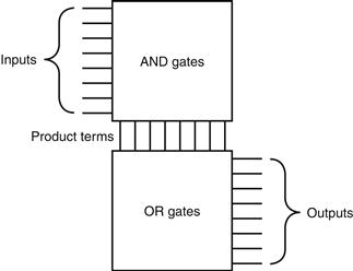
FIGURE B.3.3 The basic form of a PLA consists of an array of AND gates followed by an array of OR gates.
Each entry in the AND gate array is a product term consisting of any number of inputs or inverted inputs. Each entry in the OR gate array is a sum term consisting of any number of these product terms.
A PLA can directly implement the truth table of a set of logic functions with multiple inputs and outputs. Since each entry where the output is true requires a product term, there will be a corresponding row in the PLA. Each output corresponds to a potential row of OR gates in the second stage. The number of OR gates corresponds to the number of truth table entries for which the output is true. The total size of a PLA, such as that shown in Figure B.3.3, is equal to the sum of the size of the AND gate array (called the AND plane) and the size of the OR gate array (called the OR plane). Looking at Figure B.3.3, we can see that the size of the AND gate array is equal to the number of inputs times the number of different product terms, and the size of the OR gate array is the number of outputs times the number of product terms.
A PLA has two characteristics that help make it an efficient way to implement a set of logic functions. First, only the truth table entries that produce a true value for at least one output have any logic gates associated with them. Second, each different product term will have only one entry in the PLA, even if the product term is used in multiple outputs. Let’s look at an example.
PLAs
Example
Consider the set of logic functions defined in the example on page B-5. Show a PLA implementation of this example for D, E, and F.
Answer
Here is the truth table we constructed earlier:
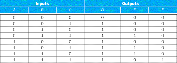
Since there are seven unique product terms with at least one true value in the output section, there will be seven columns in the AND plane. The number of rows in the AND plane is three (since there are three inputs), and there are also three rows in the OR plane (since there are three outputs). Figure B.3.4 shows the resulting PLA, with the product terms corresponding to the truth table entries from top to bottom.
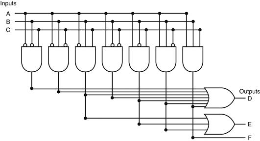
FIGURE B.3.4 The PLA for implementing the logic function described in the example.
Rather than drawing all the gates, as we do in Figure B.3.4, designers often show just the position of AND gates and OR gates. Dots are used on the intersection of a product term signal line and an input line or an output line when a corresponding AND gate or OR gate is required. Figure B.3.5 shows how the PLA of Figure B.3.4 would look when drawn in this way. The contents of a PLA are fixed when the PLA is created, although there are also forms of PLA-like structures, called PALs, that can be programmed electronically when a designer is ready to use them.
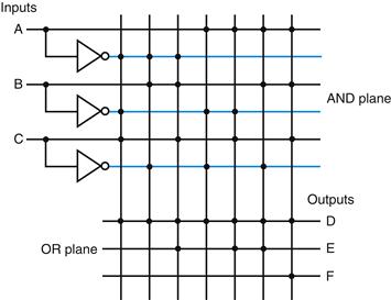
FIGURE B.3.5 A PLA drawn using dots to indicate the components of the product terms and sum terms in the array.
Rather than use inverters on the gates, usually all the inputs are run the width of the AND plane in both true and complement forms. A dot in the AND plane indicates that the input, or its inverse, occurs in the product term. A dot in the OR plane indicates that the corresponding product term appears in the corresponding output.
ROMs
Another form of structured logic that can be used to implement a set of logic functions is a read-only memory (ROM). A ROM is called a memory because it has a set of locations that can be read; however, the contents of these locations are fixed, usually at the time the ROM is manufactured. There are also programmable ROMs (PROMs) that can be programmed electronically, when a designer knows their contents. There are also erasable PROMs; these devices require a slow erasure process using ultraviolet light, and thus are used as read-only memories, except during the design and debugging process.
read-only memory (ROM)
A memory whose contents are designated at creation time, after which the contents can only be read. ROM is used as structured logic to implement a set of logic functions by using the terms in the logic functions as address inputs and the out puts as bits in each word of the memory.
programmable ROM (PROM)
A form of read-only memory that can be pro grammed when a designer knows its contents.
A ROM has a set of input address lines and a set of outputs. The number of addressable entries in the ROM determines the number of address lines: if the ROM contains 2m addressable entries, called the height, then there are m input lines. The number of bits in each addressable entry is equal to the number of output bits and is sometimes called the width of the ROM. The total number of bits in the ROM is equal to the height times the width. The height and width are sometimes collectively referred to as the shape of the ROM.
A ROM can encode a collection of logic functions directly from the truth table. For example, if there are n functions with m inputs, we need a ROM with m address lines (and 2m entries), with each entry being n bits wide. The entries in the input portion of the truth table represent the addresses of the entries in the ROM, while the contents of the output portion of the truth table constitute the contents of the ROM. If the truth table is organized so that the sequence of entries in the input portion constitutes a sequence of binary numbers (as have all the truth tables we have shown so far), then the output portion gives the ROM contents in order as well. In the example starting on page B-13, there were three inputs and three outputs. This leads to a ROM with 23 = 8 entries, each 3 bits wide. The contents of those entries in increasing order by address are directly given by the output portion of the truth table that appears on page B-14.
ROMs and PLAs are closely related. A ROM is fully decoded: it contains a full output word for every possible input combination. A PLA is only partially decoded. This means that a ROM will always contain more entries. For the earlier truth table on page B-14, the ROM contains entries for all eight possible inputs, whereas the PLA contains only the seven active product terms. As the number of inputs grows, the number of entries in the ROM grows exponentially. In contrast, for most real logic functions, the number of product terms grows much more slowly (see the examples in ![]() Appendix D). This difference makes PLAs generally more efficient for implementing combinational logic functions. ROMs have the advantage of being able to implement any logic function with the matching number of inputs and outputs. This advantage makes it easier to change the ROM contents if the logic function changes, since the size of the ROM need not change.
Appendix D). This difference makes PLAs generally more efficient for implementing combinational logic functions. ROMs have the advantage of being able to implement any logic function with the matching number of inputs and outputs. This advantage makes it easier to change the ROM contents if the logic function changes, since the size of the ROM need not change.
In addition to ROMs and PLAs, modern logic synthesis systems will also translate small blocks of combinational logic into a collection of gates that can be placed and wired automatically. Although some small collections of gates are usually not area efficient, for small logic functions they have less overhead than the rigid structure of a ROM and PLA and so are preferred.
For designing logic outside of a custom or semicustom integrated circuit, a common choice is a field programming device; we describe these devices in Section B.12.
Don’t Cares
Often in implementing some combinational logic, there are situations where we do not care what the value of some output is, either because another output is true or because a subset of the input combinations determines the values of the out puts. Such situations are referred to as don’t cares. Don’t cares are important because they make it easier to optimize the implementation of a logic function.
There are two types of don’t cares: output don’t cares and input don’t cares, both of which can be represented in a truth table. Output don’t cares arise when we don’t care about the value of an output for some input combination. They appear as Xs in the output portion of a truth table. When an output is a don’t care for some input combination, the designer or logic optimization program is free to make the output true or false for that input combination. Input don’t cares arise when an output depends on only some of the inputs, and they are also shown as Xs, though in the input portion of the truth table.
Don’t Cares
Example
Consider a logic function with inputs A, B, and C defined as follows:
■ If A or C is true, then output D is true, whatever the value of B.
■ If A or B is true, then output E is true, whatever the value of C.
■ Output F is true if exactly one of the inputs is true, although we don’t care about the value of F, whenever D and E are both true.
Show the full truth table for this function and the truth table using don’t cares. How many product terms are required in a PLA for each of these?
Answer
Here’s the full truth table, without don’t cares:
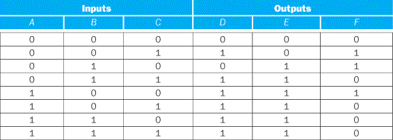
This requires seven product terms without optimization. The truth table written with output don’t cares looks like this:
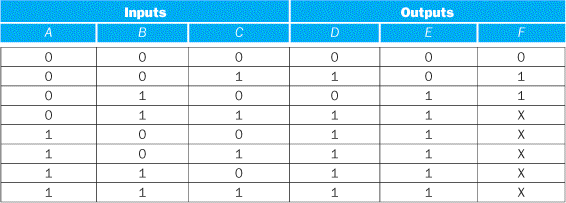
If we also use the input don’t cares, this truth table can be further simplified to yield the following:

This simplified truth table requires a PLA with four minterms, or it can be implemented in discrete gates with one two-input AND gate and three OR gates (two with three inputs and one with two inputs). This compares to the original truth table that had seven minterms and would have required four AND gates.
Logic minimization is critical to achieving efficient implementations. One tool useful for hand minimization of random logic is Karnaugh maps. Karnaugh maps represent the truth table graphically, so that product terms that may be combined are easily seen. Nevertheless, hand optimization of significant logic functions using Karnaugh maps is impractical, both because of the size of the maps and their complexity. Fortunately, the process of logic minimization is highly mechanical and can be performed by design tools. In the process of minimization, the tools take advantage of the don’t cares, so specifying them is important. The text book references at the end of this Appendix provide further discussion on logic minimization, Karnaugh maps, and the theory behind such minimization algorithms.
Arrays of Logic Elements
Many of the combinational operations to be performed on data have to be done to an entire word (32 bits) of data. Thus we often want to build an array of logic elements, which we can represent simply by showing that a given operation will hap pen to an entire collection of inputs. For example, we saw on page B-9 what a 1-bit multiplexor looked like, but inside a machine, much of the time we want to select between a pair of buses. A bus is a collection of data lines that is treated together as a single logical signal. (The term bus is also used to indicate a shared collection of lines with multiple sources and uses, especially in Chapter 6, where I/O buses were discussed.)
bus
In logic design, a collection of data lines that is treated together as a single logical signal; also, a shared collection of lines with multiple sources and uses.
For example, in the MIPS instruction set, the result of an instruction that is written into a register can come from one of two sources. A multiplexor is used to choose which of the two buses (each 32 bits wide) will be written into the Result register. The 1-bit multiplexor, which we showed earlier, will need to be replicated 32 times.
We indicate that a signal is a bus rather than a single 1-bit line by showing it with a thicker line in a figure. Most buses are 32 bits wide; those that are not are explicitly labeled with their width. When we show a logic unit whose inputs and outputs are buses, this means that the unit must be replicated a sufficient number of times to accommodate the width of the input. Figure B.3.6 shows how we draw a multiplexor that selects between a pair of 32-bit buses and how this expands in terms of 1-bit-wide multiplexors. Sometimes we need to construct an array of logic elements where the inputs for some elements in the array are outputs from earlier elements. For example, this is how a multibit-wide ALU is constructed. In such cases, we must explicitly show how to create wider arrays, since the individual elements of the array are no longer independent, as they are in the case of a 32-bit-wide multiplexor.
Check Yourself
Parity is a function in which the output depends on the number of 1s in the input. For an even parity function, the output is 1 if the input has an even number of ones. Suppose a ROM is used to implement an even parity function with a 4-bit input. Which of A, B, C, or D represents the contents of the ROM?
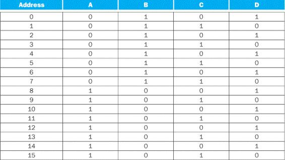
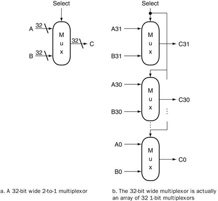
FIGURE B.3.6 A multiplexor is arrayed 32 times to perform a selection between two 32-bit inputs.
Note that there is still only one data selection signal used for all 32 1-bit multiplexors.
B.4 Using a Hardware Description Language
Today most digital design of processors and related hardware systems is done using a hardware description language. Such a language serves two purposes. First, it provides an abstract description of the hardware to simulate and debug the design. Second, with the use of logic synthesis and hardware compilation tools, this description can be compiled into the hardware implementation.
hardware description language
A programming lan guage for describing hardware, used for generating simulations of a hardware design and also as input to synthesis tools that can generate actual hardware.
In this section, we introduce the hardware description language Verilog and show how it can be used for combinational design. In the rest of the appendix, we expand the use of Verilog to include design of sequential logic. In the optional sections of Chapter 4 that appear on the CD, we use Verilog to describe processor implementations. In the optional section from Chapter 5 that appears on the CD, we use system Verilog to describe cache controller implementations. System Verilog adds structures and some other useful features to Verilog.
Verilog is one of the two primary hardware description languages; the other is VHDL. Verilog is somewhat more heavily used in industry and is based on C, as opposed to VHDL, which is based on Ada. The reader generally familiar with C will find the basics of Verilog, which we use in this appendix, easy to follow. Readers already familiar with VHDL should find the concepts simple, provided they have been exposed to the syntax of C.
Verilog
One of the two most common hardware description languages.
VHDL
One of the two most common hardware description languages.
Verilog can specify both a behavioral and a structural definition of a digital system. A behavioral specification describes how a digital system functionally operates. A structural specification describes the detailed organization of a digital system, usually using a hierarchical description. A structural specification can be used to describe a hardware system in terms of a hierarchy of basic elements such as gates and switches. Thus, we could use Verilog to describe the exact contents of the truth tables and datapath of the last section.
behavioral specification
Describes how a digital system operates functionally.
structural specification
Describes how a digital system is organized in terms of a hierarchical connection of elements.
With the arrival of hardware synthesis tools, most designers now use Verilog or VHDL to structurally describe only the datapath, relying on logic synthesis to generate the control from a behavioral description. In addition, most CAD systems provide extensive libraries of standardized parts, such as ALUs, multiplexors, register files, memories, and programmable logic blocks, as well as basic gates.
hardware synthesis tools
Computer-aided design software that can generate a gate-level design based on behavioral descriptions of a digital system.
Obtaining an acceptable result using libraries and logic synthesis requires that the specification be written with an eye toward the eventual synthesis and the desired outcome. For our simple designs, this primarily means making clear what we expect to be implemented in combinational logic and what we expect to require sequential logic. In most of the examples we use in this section and the remainder of this appendix, we have written the Verilog with the eventual synthesis in mind.
Datatypes and Operators in Verilog
There are two primary datatypes in Verilog:
1. A wire specifies a combinational signal.
2. A reg (register) holds a value, which can vary with time. A reg need not necessarily correspond to an actual register in an implementation, although it often will.
wire
In Verilog, specifies a combinational signal.
reg
In Verilog, a register.
A register or wire, named X, that is 32 bits wide is declared as an array: reg [31:0] X or wire [31:0] X, which also sets the index of 0 to designate the least significant bit of the register. Because we often want to access a subfield of a register or wire, we can refer to a contiguous set of bits of a register or wire with the notation [starting bit: ending bit], where both indices must be constant values.
An array of registers is used for a structure like a register file or memory. Thus, the declaration
reg [31:0] registerfile[0:31]
specifies a variable registerfile that is equivalent to a MIPS registerfile, where register 0 is the first. When accessing an array, we can refer to a single element, as in C, using the notation registerfile[regnum].
The possible values for a register or wire in Verilog are
■ 0 or 1, representing logical false or true
■ X, representing unknown, the initial value given to all registers and to any wire not connected to something
■ Z, representing the high-impedance state for tristate gates, which we will not discuss in this appendix
Constant values can be specified as decimal numbers as well as binary, octal, or hexadecimal. We often want to say exactly how large a constant field is in bits. This is done by prefixing the value with a decimal number specifying its size in bits. For example:
■ 4’b0100 specifies a 4-bit binary constant with the value 4, as does 4’d4.
■ - 8 ‘h4 specifies an 8-bit constant with the value −4 (in two’s complement representation)
Values can also be concatenated by placing them within { } separated by commas. The notation {x {bit field}} replicates bit field x times. For example:
■ {16{2’b01}} creates a 32-bit value with the pattern 0101 … 01.
■ {A[31:16],B[15:0]} creates a value whose upper 16 bits come from A and whose lower 16 bits come from B.
Verilog provides the full set of unary and binary operators from C, including the arithmetic operators (+, −, *. /), the logical operators (&, |, ∼), the comparison operators (= =, !=, >, <, < =, > =), the shift operators (<<, >>), and C’s conditional operator (?, which is used in the form condition ? expr1 :expr2 and returns expr1 if the condition is true and expr2 if it is false). Verilog adds a set of unary logic reduction operators (&, |, ^) that yield a single bit by applying the logical operator to all the bits of an operand. For example, &A returns the value obtained by ANDing all the bits of A together, and ^A returns the reduction obtained by using exclusive OR on all the bits of A.
Check Yourself
Which of the following define exactly the same value?
l. 8’bimoooo
2. 8’hF0
3. 8’d240
4. {{4{1’b1}},{4{1’b0}}}
5. {4’b1,4’b0)
Structure of a Verilog Program
A Verilog program is structured as a set of modules, which may represent anything from a collection of logic gates to a complete system. Modules are similar to classes in C11, although not nearly as powerful. A module specifies its input and output ports, which describe the incoming and outgoing connections of a module. A module may also declare additional variables. The body of a module consists of:
■ initial constructs, which can initialize reg variables
■ Continuous assignments, which define only combinational logic
■ always constructs, which can define either sequential or combinational logic
■ Instances of other modules, which are used to implement the module being defined
Representing Complex Combinational Logic in Verilog
A continuous assignment, which is indicated with the keyword assign, acts like a combinational logic function: the output is continuously assigned the value, and a change in the input values is reflected immediately in the output value. Wires may only be assigned values with continuous assignments. Using continuous assignments, we can define a module that implements a half-adder, as Figure B.4.1 shows.

FIGURE B.4.1 A Verilog module that defines a half-adder using continuous assignments.
Assign statements are one sure way to write Verilog that generates combina tional logic. For more complex structures, however, assign statements may be awkward or tedious to use. It is also possible to use the always block of a module to describe a combinational logic element, although care must be taken. Using an always block allows the inclusion of Verilog control constructs, such as if-then–else, case statements, for statements, and repeat statements, to be used. These state ments are similar to those in C with small changes.
An always block specifies an optional list of signals on which the block is sensitive (in a list starting with @). The always block is reevaluated if any of the listed signals changes value; if the list is omitted, the always block is constantly reevaluated. When an always block is specifying combinational logic, the sensitivity list should include all the input signals. If there are multiple Verilog statements to be executed in an always block, they are surrounded by the keywords begin and end, which take the place of the { and } in C. An always block thus looks like this:
always @(list of signals that cause reevaluation) begin Verilog statements including assignments and other control statements end
sensitivity list
The list of signals that specifies when an always block should be reevaluated.
Reg variables may only be assigned inside an always block, using a procedural assignment statement (as distinguished from continuous assignment we saw earlier). There are, however, two different types of procedural assignments. The assignment operator = executes as it does in C; the right-hand side is evaluated, and the left-hand side is assigned the value. Furthermore, it executes like the normal C assignment statement: that is, it is completed before the next statement is executed. Hence, the assignment operator = has the name blocking assignment. This blocking can be useful in the generation of sequential logic, and we will return to it shortly. The other form of assignment (nonblocking) is indicated by <=. In nonblocking assignment, all right-hand sides of the assignments in an always group are evaluated and the assignments are done simultaneously. As a first example of combinational logic implemented using an always block, Figure B.4.2 shows the implementation of a 4-to-1 multiplexor, which uses a case construct to make it easy to write. The case construct looks like a C switch statement. Figure B.4.3 shows a definition of a MIPS ALU, which also uses a case statement.
blocking assignment
In Verilog, an assignment that completes before the execution of the next statement.
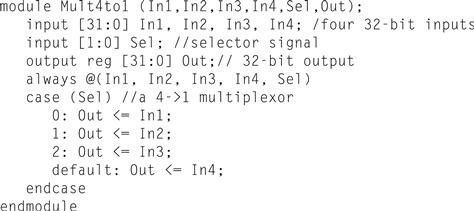
FIGURE B.4.2 A Verilog definition of a 4-to-1 multiplexor with 32-bit inputs, using a case statement.
The case statement acts like a C switch statement, except that in Verilog only the code associated with the selected case is executed (as if each case state had a break at the end) and there is no fallthrough to the next statement.
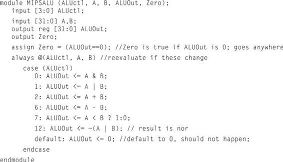
FIGURE B.4.3 A Verilog behavioral definition of a MIPS ALU.
This could be synthesized using a module library containing basic arithmetic and logical operations.
Since only reg variables may be assigned inside always blocks, when we want to describe combinational logic using an always block, care must be taken to ensure that the reg does not synthesize into a register. A variety of pitfalls are described in the elaboration below.
nonblocking assignment
An assignment that continues after evaluating the right-hand side, assigning the left-hand side the value only after all right-hand sides are evaluated.
Elaboration
Continuous assignment statements always yield combinational logic, but other Verilog structures, even when in always blocks, can yield unexpected results during logic synthesis. The most common problem is creating sequential logic by implying the existence of a latch or register, which results in an implementation that is both slower and more costly than perhaps intended. To ensure that the logic that you intend to be combinational is synthesized that way, make sure you do the following:
1. Place all combinational logic in a continuous assignment or an always block.
2. Make sure that all the signals used as inputs appear in the sensitivity list of an always block.
3. Ensure that every path through an always block assigns a value to the exact same set of bits.
The last of these is the easiest to overlook; read through the example in Figure B.5.15 to convince yourself that this property is adhered to.
Check Yourself
Assuming all values are initially zero, what are the values of A and B after executing this Verilog code inside an always block?
C=1;
A <= C;
B = C;
B.5 Constructing a Basic Arithmetic Logic Unit
The arithmetic logic unit (ALU) is the brawn of the computer, the device that per forms the arithmetic operations like addition and subtraction or logical operations like AND and OR. This section constructs an ALU from four hardware building blocks (AND and OR gates, inverters, and multiplexors) and illustrates how combinational logic works. In the next section, we will see how addition can be sped up through more clever designs.
ALU n. [Arthritic Logic Unit or (rare) Arithmetic Logic Unit]
A random-number generator supplied as standard with all computer systems.
Stan Kelly-Bootle, The Devil’s DP Dictionary, 1981
Because the MIPS word is 32 bits wide, we need a 32-bit-wide ALU. Let’s assume that we will connect 32 1-bit ALUs to create the desired ALU. We’ll therefore start by constructing a 1-bit ALU.
A 1-Bit ALU
The logical operations are easiest, because they map directly onto the hardware components in Figure B.2.1.
The 1-bit logical unit for AND and OR looks like Figure B.5.1. The multiplexor on the right then selects a AND b or a OR b, depending on whether the value of Operation is 0 or 1. The line that controls the multiplexor is shown in color to distinguish it from the lines containing data. Notice that we have renamed the control and output lines of the multiplexor to give them names that reflect the function of the ALU.
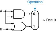
FIGURE B.5.1 The 1-bit logical unit for AND and OR.
The next function to include is addition. An adder must have two inputs for the operands and a single-bit output for the sum. There must be a second output to pass on the carry, called CarryOut. Since the CarryOut from the neighbor adder must be included as an input, we need a third input. This input is called CarryIn. Figure B.5.2 shows the inputs and the outputs of a 1-bit adder. Since we know what addition is supposed to do, we can specify the outputs of this “black box” based on its inputs, as Figure B.5.3 demonstrates.
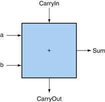
FIGURE B.5.2 A 1-bit adder.
This adder is called a full adder; it is also called a (3,2) adder because it has 3 inputs and 2 outputs. An adder with only the a and b inputs is called a (2,2) adder or half-adder
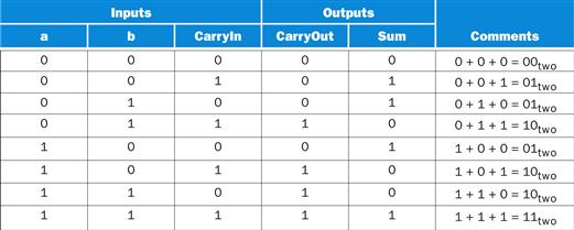
FIGURE B.5.3 Input and output specification for a 1-bit adder.
We can express the output functions Carry Out and Sum as logical equations, and these equations can in turn be implemented with logic gates. Let’s do CarryOut. Figure B.5.4 shows the values of the inputs when CarryOut is a 1.
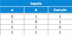
FIGURE B.5.4 Values of the inputs when CarryOut is a 1.
We can turn this truth table into a logical equation:
![]()
If a · b · CarryIn is true, then all of the other three terms must also be true, so we can leave out this last term corresponding to the fourth line of the table. We can thus simplify the equation to
![]()
Figure B.5.5 shows that the hardware within the adder black box for CarryOut consists of three AND gates and one OR gate. The three AND gates correspond exactly to the three parenthesized terms of the formula above for CarryOut, and the OR gate sums the three terms.
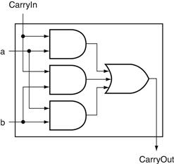
FIGURE B.5.5 Adder hardware for the CarryOut signal.
The rest of the adder hardware is the logic for the Sum output given in the equation on this page.
The Sum bit is set when exactly one input is 1 or when all three inputs are 1. The Sum results in a complex Boolean equation (recall that ![]() means NOT a):
means NOT a):
![]()
The drawing of the logic for the Sum bit in the adder black box is left as an exercise for the reader.
Figure B.5.6 shows a 1-bit ALU derived by combining the adder with the earlier components. Sometimes designers also want the ALU to perform a few more simple operations, such as generating 0. The easiest way to add an operation is to expand the multiplexor controlled by the Operation line and, for this example, to connect 0 directly to the new input of that expanded multiplexor.
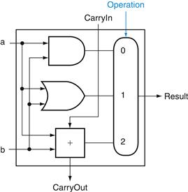
FIGURE B.5.6 A 1-bit ALU that performs AND, OR, and addition (see Figure B.5.5).
A 32-Bit ALU
Now that we have completed the 1-bit ALU, the full 32-bit ALU is created by connecting adjacent “black boxes.” Using xi to mean the ith bit of x, Figure B.5.7 shows a 32-bit ALU. Just as a single stone can cause ripples to radiate to the shores of a quiet lake, a single carry out of the least significant bit (Result0) can ripple all the way through the adder, causing a carry out of the most significant bit (Result31). Hence, the adder created by directly linking the carries of 1-bit adders is called a ripple carry adder. We’ll see a faster way to connect the 1-bit adders starting on page B-38.
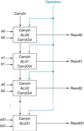
FIGURE B.5.7 A 32-bit ALU constructed from 32 1-bit ALUs.
CarryOut of the less significant bit is connected to the CarryIn of the more significant bit. This organization is called ripple carry.
Subtraction is the same as adding the negative version of an operand, and this is how adders perform subtraction. Recall that the shortcut for negating a two’s complement number is to invert each bit (sometimes called the one’s complement) and then add 1. To invert each bit, we simply add a 2:1 multiplexor that chooses between b and ![]() , as Figure B.5.8 shows.
, as Figure B.5.8 shows.
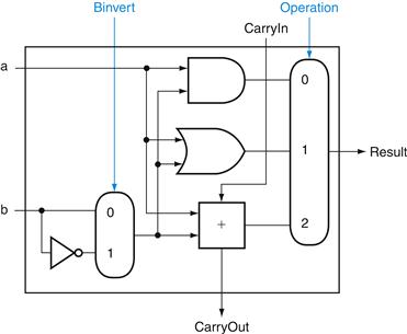
FIGURE B.5.8 A 1-bit ALU that performs AND, OR, and addition on a and b or a and ![]() .
.
By selecting ![]() (Binvert = 1) and setting CarryIn to 1 in the least significant bit of the ALU, we get two’s complement subtraction of b from a instead of addition of b to a.
(Binvert = 1) and setting CarryIn to 1 in the least significant bit of the ALU, we get two’s complement subtraction of b from a instead of addition of b to a.
Suppose we connect 32 of these 1-bit ALUs, as we did in Figure B.5.7. The added multiplexor gives the option of b or its inverted value, depending on Binvert, but this is only one step in negating a two’s complement number. Notice that the least significant bit still has a CarryIn signal, even though it’s unnecessary for addition. What happens if we set this CarryIn to 1 instead of 0? The adder will then calculate a + b + 1. By selecting the inverted version of b, we get exactly what we want:
![]()
The simplicity of the hardware design of a two’s complement adder helps explain why two’s complement representation has become the universal standard for integer computer arithmetic.
A MIPS ALU also needs a NOR function. Instead of adding a separate gate for NOR, we can reuse much of the hardware already in the ALU, like we did for subtract. The insight comes from the following truth about NOR:
![]()
That is, NOT (a OR b) is equivalent to NOT a AND NOT b. This fact is called DeMorgan’s theorem and is explored in the exercises in more depth.
Since we have AND and NOT b, we only need to add NOT a to the ALU. Figure B.5.9 shows that change.
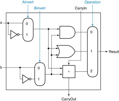
FIGURE B.5.9 A 1-bit ALU that performs AND, OR, and addition on a and b or a and b.
By selecting ![]() (Ainvert = 1) and
(Ainvert = 1) and ![]() (Binvert = 1), we get a NOR b instead of a AND b.
(Binvert = 1), we get a NOR b instead of a AND b.
Tailoring the 32-Bit ALU to MIPS
These four operations—add, subtract, AND, OR—are found in the ALU of almost every computer, and the operations of most MIPS instructions can be performed by this ALU. But the design of the ALU is incomplete.
One instruction that still needs support is the set on less than instruction (slt). Recall that the operation produces 1 if rs , rt, and 0 otherwise. Consequently, slt will set all but the least significant bit to 0, with the least significant bit set according to the comparison. For the ALU to perform slt, we first need to expand the three-input multiplexor in Figure B.5.8 to add an input for the slt result. We call that new input Less and use it only for slt.
The top drawing of Figure B.5.10 shows the new 1-bit ALU with the expanded multiplexor. From the description of slt above, we must connect 0 to the Less input for the upper 31 bits of the ALU, since those bits are always set to 0. What remains to consider is how to compare and set the least significant bit for set on less than instructions.
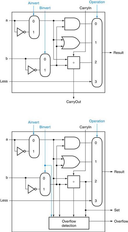
FIGURE B.5.10 (Top) A 1-bit ALU that performs AND, OR, and addition on a and b or b , and (bottom) a 1-bit ALU for the most significant bit.
The top drawing includes a direct input that is connected to perform the set on less than operation (see Figure B.5.11); the bottom has a direct output from the adder for the less than comparison called Set. (See Exercise B.24 at the end of this Appendix to see how to calculate overflow with fewer inputs.)
What happens if we subtract b from a? If the difference is negative, then a < b since
![]()
We want the least significant bit of a set on less than operation to be a 1 if a < b; that is, a 1 if a − b is negative and a 0 if it’s positive. This desired result corresponds exactly to the sign bit values: 1 means negative and 0 means positive. Following this line of argument, we need only connect the sign bit from the adder output to the least significant bit to get set on less than.
Unfortunately, the Result output from the most significant ALU bit in the top of Figure B.5.10 for the slt operation is not the output of the adder; the ALU output for the slt operation is obviously the input value Less.
Thus, we need a new 1-bit ALU for the most significant bit that has an extra output bit: the adder output. The bottom drawing of Figure B.5.10 shows the design, with this new adder output line called Set, and used only for slt. As long as we need a special ALU for the most significant bit, we added the overflow detec tion logic since it is also associated with that bit.
Alas, the test of less than is a little more complicated than just described because of overflow, as we explore in the exercises. Figure B.5.11 shows the 32-bit ALU.
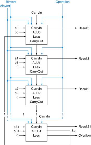
FIGURE B.5.11 A 32-bit ALU constructed from the 31 copies of the 1-bit ALU in the top of Figure B.5.10 and one 1-bit ALU in the bottom of that figure.
The Less inputs are connected to 0 except for the least significant bit, which is connected to the Set output of the most significant bit. If the ALU performs a − b and we select the input 3 in the multiplexor in Figure B.5.10, then Result = 0 … 001 if a < b, and Result = 0 … 000 otherwise.
Notice that every time we want the ALU to subtract, we set both CarryIn and Binvert to 1. For adds or logical operations, we want both control lines to be 0. We can therefore simplify control of the ALU by combining the CarryIn and Binvert to a single control line called Bnegate.
To further tailor the ALU to the MIPS instruction set, we must support conditional branch instructions. These instructions branch either if two registers are equal or if they are unequal. The easiest way to test equality with the ALU is to subtract b from a and then test to see if the result is 0, since
![]()
Thus, if we add hardware to test if the result is 0, we can test for equality. The simplest way is to OR all the outputs together and then send that signal through an inverter:
![]()
Figure B.5.12 shows the revised 32-bit ALU. We can think of the combination of the 1-bit Ainvert line, the 1-bit Binvert line, and the 2-bit Operation lines as 4-bit control lines for the ALU, telling it to perform add, subtract, AND, OR, or set on less than. Figure B.5.13 shows the ALU control lines and the corresponding ALU operation.
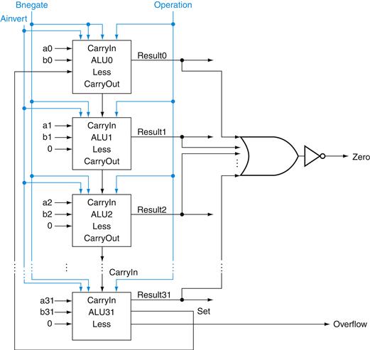
FIGURE B.5.12 The final 32-bit ALU.
This adds a Zero detector to Figure B.5.11.
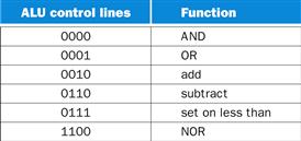
FIGURE B.5.13 The values of the three ALU control lines, Bnegate, and Operation, and the corresponding ALU operations.
Finally, now that we have seen what is inside a 32-bit ALU, we will use the universal symbol for a complete ALU, as shown in Figure B.5.14.
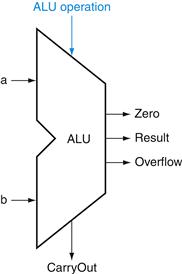
FIGURE B.5.14 The symbol commonly used to represent an ALU, as shown in Figure B.5.12.
This symbol is also used to represent an adder, so it is normally labeled either with ALU or Adder.
Defining the MIPS ALU in Verilog
Figure B.5.15 shows how a combinational MIPS ALU might be specified in Verilog; such a specification would probably be compiled using a standard parts library that provided an adder, which could be instantiated. For completeness, we show the ALU control for MIPS in Figure B.5.16, which is used in Chapter 4, where we build a Verilog version of the MIPS datapath.
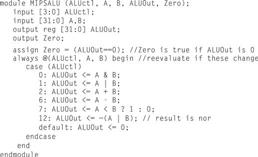
FIGURE B.5.15 A Verilog behavioral definition of a MIPS ALU.
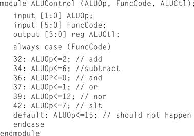
FIGURE B.5.16 The MIPS ALU control: a simple piece of combinational control logic.
The next question is, “How quickly can this ALU add two 32-bit operands?” We can determine the a and b inputs, but the CarryIn input depends on the operation in the adjacent 1-bit adder. If we trace all the way through the chain of dependencies, we connect the most significant bit to the least significant bit, so the most significant bit of the sum must wait for the sequential evaluation of all 32 1-bit adders. This sequential chain reaction is too slow to be used in time-critical hardware. The next section explores how to speed-up addition. This topic is not crucial to understanding the rest of the appendix and may be skipped.
Check Yourself
Suppose you wanted to add the operation NOT (a AND b), called NAND. How could the ALU change to support it?
1. No change. You can calculate NAND quickly using the current ALU since ![]() and we already have NOT a, NOT b, and OR.
and we already have NOT a, NOT b, and OR.
2. You must expand the big multiplexor to add another input, and then add new logic to calculate NAND.
B.6 Faster Addition: Carry Lookahead
The key to speeding up addition is determining the carry in to the high-order bits sooner. There are a variety of schemes to anticipate the carry so that the worst-case scenario is a function of the log2 of the number of bits in the adder. These anticipatory signals are faster because they go through fewer gates in sequence, but it takes many more gates to anticipate the proper carry.
A key to understanding fast-carry schemes is to remember that, unlike soft ware, hardware executes in parallel whenever inputs change.
Fast Carry Using “Infinite” Hardware
As we mentioned earlier, any equation can be represented in two levels of logic. Since the only external inputs are the two operands and the CarryIn to the least significant bit of the adder, in theory we could calculate the CarryIn values to all the remaining bits of the adder in just two levels of logic.
For example, the CarryIn for bit 2 of the adder is exactly the CarryOut of bit 1, so the formula is
![]()
Similarly, CarryIn1 is defined as
![]()
Using the shorter and more traditional abbreviation of ci for CarryIni, we can rewrite the formulas as
![]()
Substituting the definition of c1 for the first equation results in this formula:
![]()
You can imagine how the equation expands as we get to higher bits in the adder; it grows rapidly with the number of bits. This complexity is reflected in the cost of the hardware for fast carry, making this simple scheme prohibitively expensive for wide adders.
Fast Carry Using the First Level of Abstraction: Propagate and Generate
Most fast-carry schemes limit the complexity of the equations to simplify the hardware, while still making substantial speed improvements over ripple carry. One such scheme is a carry-lookahead adder. In Chapter 1, we said computer systems cope with complexity by using levels of abstraction. A carry-lookahead adder relies on levels of abstraction in its implementation.
Let’s factor our original equation as a first step:
![]()
If we were to rewrite the equation for c2 using this formula, we would see some repeated patterns:
![]()
Note the repeated appearance of (ai · bi) and (ai + bi) in the formula above. These two important factors are traditionally called generate (gi) and propagate (pi):
![]()
Using them to define ci + 1, we get
![]()
To see where the signals get their names, suppose gi is 1. Then
![]()
That is, the adder generates a CarryOut (ci + 1) independent of the value of Car ryIn (ci). Now suppose that gi is 0 and pi is 1. Then
![]()
That is, the adder propagates CarryIn to a CarryOut. Putting the two together, CarryIni + 1 is a 1 if either gi is 1 or both pi is 1 and CarryIni is 1.
As an analogy, imagine a row of dominoes set on edge. The end domino can be tipped over by pushing one far away, provided there are no gaps between the two. Similarly, a carry out can be made true by a generate far away, provided all the propagates between them are true.
Relying on the definitions of propagate and generate as our first level of abstraction, we can express the CarryIn signals more economically. Let’s show it for 4 bits:
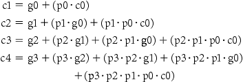
These equations just represent common sense: CarryIni is a 1 if some earlier adder generates a carry and all intermediary adders propagate a carry. Figure B.6.1 uses plumbing to try to explain carry lookahead.
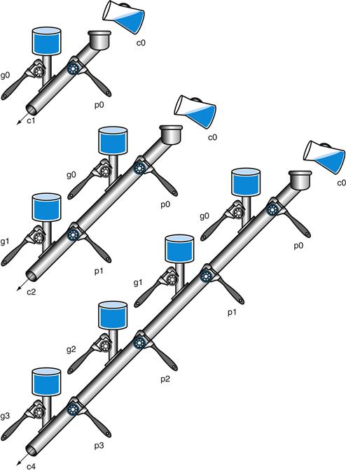
FIGURE B.6.1 A plumbing analogy for carry lookahead for 1 bit, 2 bits, and 4 bits using water pipes and valves.
The wrenches are turned to open and close valves. Water is shown in color. The output of the pipe (ci + 1) will be full if either the nearest generate value (gi) is turned on or if the i propagate value (pi) is on and there is water further upstream, either from an earlier generate or a propagate with water behind it. CarryIn (c0) can result in a carry out without the help of any generates, but with the help of all propagates.
Even this simplified form leads to large equations and, hence, considerable logic even for a 16-bit adder. Let’s try moving to two levels of abstraction.
Fast Carry Using the Second Level of Abstraction
First, we consider this 4-bit adder with its carry-lookahead logic as a single building block. If we connect them in ripple carry fashion to form a 16-bit adder, the add will be faster than the original with a little more hardware.
To go faster, we’ll need carry lookahead at a higher level. To perform carry look ahead for 4-bit adders, we need to propagate and generate signals at this higher level. Here they are for the four 4-bit adder blocks:

That is, the “super” propagate signal for the 4-bit abstraction (Pi) is true only if each of the bits in the group will propagate a carry.
For the “super” generate signal (Gi), we care only if there is a carry out of the most significant bit of the 4-bit group. This obviously occurs if generate is true for that most significant bit; it also occurs if an earlier generate is true and all the intermediate propagates, including that of the most significant bit, are also true:

Figure B.6.2 updates our plumbing analogy to show P0 and G0.
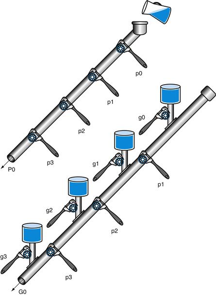
FIGURE B.6.2 A plumbing analogy for the next-level carry-lookahead signals P0 and G0.
P0 is open only if all four propagates (pi) are open, while water flows in G0 only if at least one generate (gi) is open and all the propagates downstream from that generate are open.
Then the equations at this higher level of abstraction for the carry in for each 4-bit group of the 16-bit adder (C1, C2, C3, C4 in Figure B.6.3) are very similar to the carry out equations for each bit of the 4-bit adder (c1, c2, c3, c4) on page B-40:

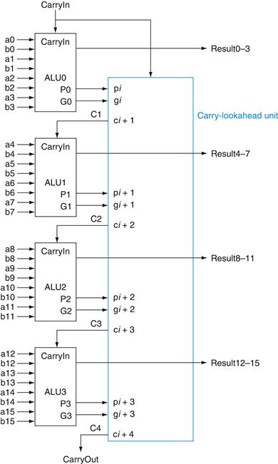
FIGURE B.6.3 Four 4-bit ALUs using carry lookahead to form a 16-bit adder.
Note that the carries come from the carry-lookahead unit, not from the 4-bit ALUs.
Figure B.6.3 shows 4-bit adders connected with such a carry-lookahead unit. The exercises explore the speed differences between these carry schemes, different notations for multibit propagate and generate signals, and the design of a 64-bit adder.
Both Levels of the Propagate and Generate
Example
Determine the gi, pi, Pi, and Gi values of these two 16-bit numbers:
![]()
Also, what is CarryOut15 (C4)?
Answer
Aligning the bits makes it easy to see the values of generate gi (ai · bi) and propagate pi (ai + bi):

where the bits are numbered 15 to 0 from left to right. Next, the “super” propagates (P3, P2, P1, P0) are simply the AND of the lower-level propagates:

The “super” generates are more complex, so use the following equations:
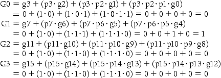
Finally, CarryOut15 is

Hence, there is a carry out when adding these two 16-bit numbers.
The reason carry lookahead can make carries faster is that all logic begins evaluating the moment the clock cycle begins, and the result will not change once the output of each gate stops changing. By taking the shortcut of going through fewer gates to send the carry in signal, the output of the gates will stop changing sooner, and hence the time for the adder can be less.
To appreciate the importance of carry lookahead, we need to calculate the relative performance between it and ripple carry adders.
Speed of Ripple Carry versus Carry Lookahead
Example
One simple way to model time for logic is to assume each AND or OR gate takes the same time for a signal to pass through it. Time is estimated by simply counting the number of gates along the path through a piece of logic. Compare the number of gate delays for paths of two 16-bit adders, one using ripple carry and one using two-level carry lookahead.
Answer
Figure B.5.5 on page B-28 shows that the carry out signal takes two gate delays per bit. Then the number of gate delays between a carry in to the least significant bit and the carry out of the most significant is 16 × 2 = 32.
For carry lookahead, the carry out of the most significant bit is just C4, defined in the example. It takes two levels of logic to specify C4 in terms of Pi and Gi (the OR of several AND terms). Pi is specified in one level of logic (AND) using pi, and Gi is specified in two levels using pi and gi, so the worst case for this next level of abstraction is two levels of logic. pi and gi are each one level of logic, defined in terms of ai and bi. If we assume one gate delay for each level of logic in these equations, the worst case is 2 + 2 + 1 = 5 gate delays.
Hence, for the path from carry in to carry out, the 16-bit addition by a carry-lookahead adder is six times faster, using this very simple estimate of hardware speed.
Summary
Carry lookahead offers a faster path than waiting for the carries to ripple through all 32 1-bit adders. This faster path is paved by two signals, generate and propagate. The former creates a carry regardless of the carry input, and the latter passes a carry along. Carry lookahead also gives another example of how abstraction is important in computer design to cope with complexity.
Check Yourself
Using the simple estimate of hardware speed above with gate delays, what is the relative performance of a ripple carry 8-bit add versus a 64-bit add using carry-lookahead logic?
1. A 64-bit carry-lookahead adder is three times faster: 8-bit adds are 16 gate delays and 64-bit adds are 7 gate delays.
2. They are about the same speed, since 64-bit adds need more levels of logic in the 16-bit adder.
3. 8-bit adds are faster than 64 bits, even with carry lookahead.
Elaboration
We have now accounted for all but one of the arithmetic and logical operations for the core MIPS instruction set: the ALU in Figure B.5.14 omits support of shift instructions. It would be possible to widen the ALU multiplexor to include a left shift by 1 bit or a right shift by 1 bit. But hardware designers have created a circuit called a barrel shifter, which can shift from 1 to 31 bits in no more time than it takes to add two 32-bit numbers, so shifting is normally done outside the ALU.
Elaboration
The logic equation for the Sum output of the full adder on page B-28 can be expressed more simply by using a more powerful gate than AND and OR. An exclusive OR gate is true if the two operands disagree; that is,
![]()
In some technologies, exclusive OR is more efficient than two levels of AND and OR gates. Using the symbol ![]() to represent exclusive OR, here is the new equation:
to represent exclusive OR, here is the new equation:
![]()
Also, we have drawn the ALU the traditional way, using gates. Computers are designed today in CMOS transistors, which are basically switches. CMOS ALU and bar rel shifters take advantage of these switches and have many fewer multiplexors than shown in our designs, but the design principles are similar.
Elaboration
Using lowercase and uppercase to distinguish the hierarchy of generate and propagate symbols breaks down when you have more than two levels. An alternate notation that scales is gi..j and pi..jfor the generate and propagate signals for bits i to j. Thus, g1..1 is generated for bit 1, g4..1 is for bits 4 to 1, and g16..1 is for bits 16 to 1.
B.7 Clocks
Before we discuss memory elements and sequential logic, it is useful to discuss briefly the topic of clocks. This short section introduces the topic and is similar to the discussion found in Section 4.2. More details on clocking and timing methodologies are presented in Section B.11.
edge-triggered clocking
A clocking scheme in which all state changes occur on a clock edge.
Clocks are needed in sequential logic to decide when an element that contains state should be updated. A clock is simply a free-running signal with a fixed cycle time; the clock frequency is simply the inverse of the cycle time. As shown in Figure B.7.1, the clock cycle time or clock period is divided into two portions: when the clock is high and when the clock is low. In this text, we use only edge-triggered clocking. This means that all state changes occur on a clock edge. We use an edge-triggered methodology because it is simpler to explain. Depending on the tech nology, it may or may not be the best choice for a clocking methodology.
clocking methodology
The approach used to determine when data is valid and stable relative to the clock.

FIGURE B.7.1 A clock signal oscillates between high and low values.
The clock period is the time for one full cycle. In an edge-triggered design, either the rising or falling edge of the clock is active and causes state to be changed.
In an edge-triggered methodology, either the rising edge or the falling edge of the clock is active and causes state changes to occur. As we will see in the next section, the state elements in an edge-triggered design are implemented so that the contents of the state elements only change on the active clock edge. The choice of which edge is active is influenced by the implementation technology and does not affect the concepts involved in designing the logic.
state element
A memory element.
The clock edge acts as a sampling signal, causing the value of the data input to a state element to be sampled and stored in the state element. Using an edge trigger means that the sampling process is essentially instantaneous, eliminating problems that could occur if signals were sampled at slightly different times.
synchronous system
A memory system that employs clocks and where data signals are read only when the clock indicates that the signal values are stable.
The major constraint in a clocked system, also called a synchronous system, is that the signals that are written into state elements must be valid when the active clock edge occurs. A signal is valid if it is stable (i.e., not changing), and the value will not change again until the inputs change. Since combinational circuits cannot have feedback, if the inputs to a combinational logic unit are not changed, the outputs will eventually become valid.
Figure B.7.2 shows the relationship among the state elements and the combinational logic blocks in a synchronous, sequential logic design. The state elements, whose outputs change only after the clock edge, provide valid inputs to the combinational logic block. To ensure that the values written into the state elements on the active clock edge are valid, the clock must have a long enough period so that all the signals in the combinational logic block stabilize, then the clock edge samples those values for storage in the state elements. This constraint sets a lower bound on the length of the clock period, which must be long enough for all state element inputs to be valid.

FIGURE B.7.2 The inputs to a combinational logic block come from a state element, and the outputs are written into a state element.
The clock edge determines when the contents of the state elements are updated.
In the rest of this appendix, as well as in Chapter 4, we usually omit the clock signal, since we are assuming that all state elements are updated on the same clock edge. Some state elements will be written on every clock edge, while others will be written only under certain conditions (such as a register being updated). In such cases, we will have an explicit write signal for that state element. The write signal must still be gated with the clock so that the update occurs only on the clock edge if the write signal is active. We will see how this is done and used in the next section.
One other advantage of an edge-triggered methodology is that it is possible to have a state element that is used as both an input and output to the same combinational logic block, as shown in Figure B.7.3. In practice, care must be taken to prevent races in such situations and to ensure that the clock period is long enough; this topic is discussed further in Section B.11.

FIGURE B.7.3 An edge-triggered methodology allows a state element to be read and written in the same clock cycle without creating a race that could lead to undetermined data values.
Of course, the clock cycle must still be long enough so that the input values are stable when the active clock edge occurs.
Now that we have discussed how clocking is used to update state elements, we can discuss how to construct the state elements.
Elaboration
Occasionally, designers find it useful to have a small number of state elements that change on the opposite clock edge from the majority of the state elements. Doing so requires extreme care, because such an approach has effects on both the inputs and the outputs of the state element. Why then would designers ever do this? Consider the case where the amount of combinational logic before and after a state element is small enough so that each could operate in one-half clock cycle, rather than the more usual full clock cycle. Then the state element can be written on the clock edge corresponding to a half clock cycle, since the inputs and outputs will both be usable after one-half clock cycle. One common place where this technique is used is in register files, where simply reading or writing the register file can often be done in half the normal clock cycle. Chapter 4 makes use of this idea to reduce the pipelining over head.
register file
A state element that consists of a set of registers that can be read and written by supplying a register number to be accessed.
B.8 Memory Elements: Flip-Flops, Latches, and Registers
In this section and the next, we discuss the basic principles behind memory elements, starting with flip-flops and latches, moving on to register files, and finishing with memories. All memory elements store state: the output from any memory element depends both on the inputs and on the value that has been stored inside the memory element. Thus all logic blocks containing a memory element contain state and are sequential.
The simplest type of memory elements are unclocked; that is, they do not have any clock input. Although we only use clocked memory elements in this text, an unclocked latch is the simplest memory element, so let’s look at this circuit first. Figure B.8.1 shows an S-R latch (set-reset latch), built from a pair of NOR gates (OR gates with inverted outputs). The outputs Q and ![]() represent the value of the stored state and its complement. When neither S nor R are asserted, the cross-coupled NOR gates act as inverters and store the previous values of Q and
represent the value of the stored state and its complement. When neither S nor R are asserted, the cross-coupled NOR gates act as inverters and store the previous values of Q and ![]() .
.
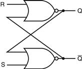
FIGURE B.8.1 A pair of cross-coupled NOR gates can store an internal value.
The value stored on the output Q is recycled by inverting it to obtain ![]() and then inverting
and then inverting ![]() to obtain Q. If either R or
to obtain Q. If either R or ![]() is asserted, Q will be deasserted and vice versa.
is asserted, Q will be deasserted and vice versa.
For example, if the output, Q, is true, then the bottom inverter produces a false output (which is ![]() ), which becomes the input to the top inverter, which produces a true output, which is Q, and so on. If S is asserted, then the output Q will be asserted and
), which becomes the input to the top inverter, which produces a true output, which is Q, and so on. If S is asserted, then the output Q will be asserted and ![]() will be deasserted, while if R is asserted, then the output
will be deasserted, while if R is asserted, then the output ![]() will be asserted and Q will be deasserted. When S and R are both deasserted, the last values of Q and
will be asserted and Q will be deasserted. When S and R are both deasserted, the last values of Q and ![]() will continue to be stored in the cross-coupled structure. Asserting S and R simultaneously can lead to incorrect operation: depending on how S and R are deasserted, the latch may oscillate or become metastable (this is described in more detail in Section B.11).
will continue to be stored in the cross-coupled structure. Asserting S and R simultaneously can lead to incorrect operation: depending on how S and R are deasserted, the latch may oscillate or become metastable (this is described in more detail in Section B.11).
This cross-coupled structure is the basis for more complex memory elements that allow us to store data signals. These elements contain additional gates used to store signal values and to cause the state to be updated only in conjunction with a clock. The next section shows how these elements are built.
Flip-Flops and Latches
Flip-flops and latches are the simplest memory elements. In both flip-flops and latches, the output is equal to the value of the stored state inside the element. Furthermore, unlike the S-R latch described above, all the latches and flip-flops we will use from this point on are clocked, which means that they have a clock input and the change of state is triggered by that clock. The difference between a flip-flop and a latch is the point at which the clock causes the state to actually change. In a clocked latch, the state is changed whenever the appropriate inputs change and the clock is asserted, whereas in a flip-flop, the state is changed only on a clock edge. Since throughout this text we use an edge-triggered timing methodology where state is only updated on clock edges, we need only use flip-flops. Flip-flops are often built from latches, so we start by describing the operation of a simple clocked latch and then discuss the operation of a flip-flop constructed from that latch.
flip-flop
A memory element for which the output is equal to the value of the stored state inside the element and for which the internal state is changed only on a clock edge.
latch
A memory element in which the output is equal to the value of the stored state inside the element and the state is changed whenever the appropriate inputs change and the clock is asserted.
For computer applications, the function of both flip-flops and latches is to store a signal. A D latch or D flip-flop stores the value of its data input signal in the internal memory. Although there are many other types of latches and flip-flops, the D type is the only basic building block that we will need. A D latch has two inputs and two outputs. The inputs are the data value to be stored (called D) and a clock signal (called C) that indicates when the latch should read the value on the D input and store it. The outputs are simply the value of the internal state (Q) and its complement (![]() ). When the clock input C is asserted, the latch is said to be open, and the value of the output (Q) becomes the value of the input D. When the clock input C is deasserted, the latch is said to be closed, and the value of the out put (Q) is whatever value was stored the last time the latch was open.
). When the clock input C is asserted, the latch is said to be open, and the value of the output (Q) becomes the value of the input D. When the clock input C is deasserted, the latch is said to be closed, and the value of the out put (Q) is whatever value was stored the last time the latch was open.
D flip-flop
A flip-flop with one data input that stores the value of that input signal in the internal memory when the clock edge occurs.
Figure B.8.2 shows how a D latch can be implemented with two additional gates added to the cross-coupled NOR gates. Since when the latch is open the value of Q changes as D changes, this structure is sometimes called a transparent latch. Figure B.8.3 shows how this D latch works, assuming that the output Q is initially false and that D changes first.
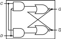
FIGURE B.8.2 A D latch implemented with NOR gates.
A NOR gate acts as an inverter if the other input is 0. Thus, the cross-coupled pair of NOR gates acts to store the state value unless the clock input, C, is asserted, in which case the value of input D replaces the value of Q and is stored. The value of input D must be stable when the clock signal C changes from asserted to deasserted.
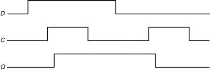
FIGURE B.8.3 Operation of a D latch, assuming the output is initially deasserted.
When the clock, C, is asserted, the latch is open and the Q output immediately assumes the value of the D input.
As mentioned earlier, we use flip-flops as the basic building block, rather than latches. Flip-flops are not transparent: their outputs change only on the clock edge. A flip-flop can be built so that it triggers on either the rising (positive) or falling (negative) clock edge; for our designs we can use either type. Figure B.8.4 shows how a falling-edge D flip-flop is constructed from a pair of D latches. In a D flip-flop, the output is stored when the clock edge occurs. Figure B.8.5 shows how this flip-flop operates.
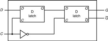
FIGURE B.8.4 A D flip-flop with a falling-edge trigger.
The first latch, called the master, is open and follows the input D when the clock input, C, is asserted. When the clock input, C, falls, the first latch is closed, but the second latch, called the slave, is open and gets its input from the output of the master latch.
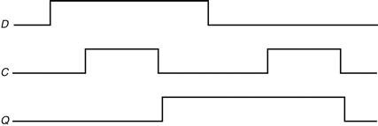
FIGURE B.8.5 Operation of a D flip-flop with a falling-edge trigger, assuming the output is initially deasserted.
When the clock input (C) changes from asserted to deasserted, the Q output stores the value of the D input. Compare this behavior to that of the clocked D latch shown in Figure B.8.3. In a clocked latch, the stored value and the output, Q, both change whenever C is high, as opposed to only when C transitions.
Here is a Verilog description of a module for a rising-edge D flip-flop, assuming that C is the clock input and D is the data input:
module DFF(clock,D,Q,Qbar);
input clock, D;
output reg Q; // Q is a reg since it is assigned in an always block
output Qbar;
assign Qbar = ~ Q; // Qbar is always just the inverse of Q
always @(posedge clock) // perform actions whenever the clock rises
Q = D;
endmodule
Because the D input is sampled on the clock edge, it must be valid for a period of time immediately before and immediately after the clock edge. The minimum time that the input must be valid before the clock edge is called the setup time; the minimum time during which it must be valid after the clock edge is called the hold time. Thus the inputs to any flip-flop (or anything built using flip-flops) must be valid during a window that begins at time tsetup before the clock edge and ends at thold after the clock edge, as shown in Figure B.8.6. Section B.11 talks about clocking and timing constraints, including the propagation delay through a flip-flop, in more detail.
hold time
The minimum time during which the input must be valid after the clock edge.
setup time
The minimum time that the input to a memory device must be valid before the clock edge.

FIGURE B.8.6 Setup and hold time requirements for a D flip-flop with a falling-edge trigger.
The input must be stable for a period of time before the clock edge, as well as after the clock edge. The minimum time the signal must be stable before the clock edge is called the setup time, while the minimum time the signal must be stable after the clock edge is called the hold time. Failure to meet these minimum require ments can result in a situation where the output of the flip-flop may not be predictable, as described in Section B.11. Hold times are usually either 0 or very small and thus not a cause of worry.
We can use an array of D flip-flops to build a register that can hold a multibit datum, such as a byte or word. We used registers throughout our datapaths in Chapter 4.
Register Files
One structure that is central to our datapath is a register file. A register file consists of a set of registers that can be read and written by supplying a register number to be accessed. A register file can be implemented with a decoder for each read or write port and an array of registers built from D flip-flops. Because reading a register does not change any state, we need only supply a register number as an input, and the only output will be the data contained in that register. For writing a register we will need three inputs: a register number, the data to write, and a clock that controls the writing into the register. In Chapter 4, we used a register file that has two read ports and one write port. This register file is drawn as shown in Figure B.8.7. The read ports can be implemented with a pair of multiplexors, each of which is as wide as the number of bits in each register of the register file. Figure B.8.8 shows the implementation of two register read ports for a 32-bit-wide register file.
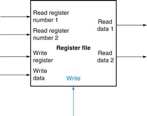
FIGURE B.8.7 A register file with two read ports and one write port has five inputs and two outputs.
The control input Write is shown in color.
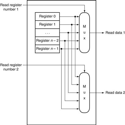
FIGURE B.8.8 The implementation of two read ports for a register file with n registers can be done with a pair of n-to-1 multiplexors, each 32 bits wide.
The register read number signal is used as the multiplexor selector signal. Figure B.8.9 shows how the write port is implemented.
Implementing the write port is slightly more complex, since we can only change the contents of the designated register. We can do this by using a decoder to generate a signal that can be used to determine which register to write. Figure B.8.9 shows how to implement the write port for a register file. It is important to remember that the flip-flop changes state only on the clock edge. In Chapter 4, we hooked up write signals for the register file explicitly and assumed the clock shown in Figure B.8.9 is attached implicitly.
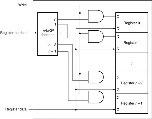
FIGURE B.8.9 The write port for a register file is implemented with a decoder that is used with the write signal to generate the C input to the registers.
All three inputs (the register number, the data, and the write signal) will have setup and hold-time constraints that ensure that the correct data is written into the register file.
What happens if the same register is read and written during a clock cycle? Because the write of the register file occurs on the clock edge, the register will be valid during the time it is read, as we saw earlier in Figure B.7.2. The value returned will be the value written in an earlier clock cycle. If we want a read to return the value currently being written, additional logic in the register file or out side of it is needed. Chapter 4 makes extensive use of such logic.
Specifying Sequential Logic in Verilog
To specify sequential logic in Verilog, we must understand how to generate a clock, how to describe when a value is written into a register, and how to specify sequential control. Let us start by specifying a clock. A clock is not a predefined object in Verilog; instead, we generate a clock by using the Verilog notation #n before a statement; this causes a delay of n simulation time steps before the execu tion of the statement. In most Verilog simulators, it is also possible to generate a clock as an external input, allowing the user to specify at simulation time the number of clock cycles during which to run a simulation.
The code in Figure B.8.10 implements a simple clock that is high or low for one simulation unit and then switches state. We use the delay capability and blocking assignment to implement the clock.
![]()
FIGURE B.8.10 A specification of a clock.
Next, we must be able to specify the operation of an edge-triggered register. In Verilog, this is done by using the sensitivity list on an always block and specifying as a trigger either the positive or negative edge of a binary variable with the notation posedge or negedge, respectively. Hence, the following Verilog code causes register A to be written with the value b at the positive edge clock:
Throughout this chapter and the Verilog sections of Chapter 4, we will assume a positive edge-triggered design. Figure B.8.11 shows a Verilog specifica tion of a MIPS register file that assumes two reads and one write, with only the write being clocked.
Check Yourself
In the Verilog for the register file in Figure B.8.11, the output ports corresponding to the registers being read are assigned using a continuous assignment, but the register being written is assigned in an always block. Which of the following is the reason?
a. There is no special reason. It was simply convenient.
b. Because Data1 and Data2 are output ports and WriteData is an input port.
c. Because reading is a combinational event, while writing is a sequential event.
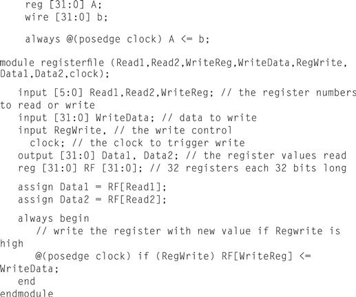
FIGURE B.8.11 A MIPS register file written in behavioral Verilog.
This register file writes on the rising clock edge.
B.9 Memory Elements: SRAMs and DRAMs
Registers and register files provide the basic building blocks for small memories, but larger amounts of memory are built using either SRAMs (static random access memories) or DRAMs (dynamic random access memories). We first discuss SRAMs, which are somewhat simpler, and then turn to DRAMs.
static random access memory (SRAM)
A memory where data is stored statically (as in flip-flops) rather than dynami cally (as in DRAM). SRAMs are faster than DRAMs, but less dense and more expensive per bit.
SRAMs
SRAMs are simply integrated circuits that are memory arrays with (usually) a single access port that can provide either a read or a write. SRAMs have a fixed access time to any datum, though the read and write access characteristics often differ. An SRAM chip has a specific configuration in terms of the number of addressable locations, as well as the width of each addressable location. For example, a 4M × 8 SRAM provides 4M entries, each of which is 8 bits wide. Thus it will have 22 address lines (since 4M = 222), an 8-bit data output line, and an 8-bit single data input line. As with ROMs, the number of addressable locations is often called the height, with the number of bits per unit called the width. For a variety of technical reasons, the newest and fastest SRAMs are typically available in narrow configurations: × 1 and × 4. Figure B.9.1 shows the input and output signals for a 2M × 16 SRAM.
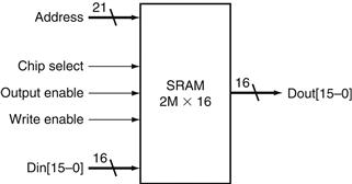
FIGURE B.9.1 A 32K × 8 SRAM showing the 21 address lines (32K = 215) and 16 data inputs, the 3 control lines, and the 16 data outputs.
To initiate a read or write access, the Chip select signal must be made active. For reads, we must also activate the Output enable signal that controls whether or not the datum selected by the address is actually driven on the pins. The Output enable is useful for connecting multiple memories to a single-output bus and using Output enable to determine which memory drives the bus. The SRAM read access time is usually specified as the delay from the time that Output enable is true and the address lines are valid until the time that the data is on the output lines. Typical read access times for SRAMs in 2004 varied from about 2–4 ns for the fastest CMOS parts, which tend to be somewhat smaller and narrower, to 8–20 ns for the typical largest parts, which in 2004 had more than 32 million bits of data. The demand for low-power SRAMs for consumer products and digital appliances has grown greatly in the past five years; these SRAMs have much lower stand-by and access power, but usually are 5–10 times slower. Most recently, synchronous SRAMs—similar to the synchronous DRAMs, which we discuss in the next section—have also been developed.
For writes, we must supply the data to be written and the address, as well as signals to cause the write to occur. When both the Write enable and Chip select are true, the data on the data input lines is written into the cell specified by the address. There are setup-time and hold-time requirements for the address and data lines, just as there were for D flip-flops and latches. In addition, the Write enable signal is not a clock edge but a pulse with a minimum width requirement. The time to complete a write is specified by the combination of the setup times, the hold times, and the Write enable pulse width.
Large SRAMs cannot be built in the same way we build a register file because, unlike a register file where a 32-to-1 multiplexor might be practical, the 64K-to-1 multiplexor that would be needed for a 64K × 1 SRAM is totally impractical. Rather than use a giant multiplexor, large memories are implemented with a shared output line, called a bit line, which multiple memory cells in the memory array can assert. To allow multiple sources to drive a single line, a three-state buffer (or tristate buffer) is used. A three-state buffer has two inputs—a data signal and an Output enable—and a single output, which is in one of three states: asserted, deasserted, or high impedance. The output of a tristate buffer is equal to the data input signal, either asserted or deasserted, if the Output enable is asserted, and is otherwise in a high-impedance state that allows another three-state buffer whose Output enable is asserted to determine the value of a shared output.
Figure B.9.2 shows a set of three-state buffers wired to form a multiplexor with a decoded input. It is critical that the Output enable of at most one of the three-state buffers be asserted; otherwise, the three-state buffers may try to set the output line differently. By using three-state buffers in the individual cells of the SRAM, each cell that corresponds to a particular output can share the same out put line. The use of a set of distributed three-state buffers is a more efficient implementation than a large centralized multiplexor. The three-state buffers are incorporated into the flip-flops that form the basic cells of the SRAM. Figure B.9.3 shows how a small 4 × 2 SRAM might be built, using D latches with an input called Enable that controls the three-state output.
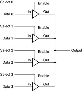
FIGURE B.9.2 Four three-state buffers are used to form a multiplexor.
Only one of the four Select inputs can be asserted. A three-state buffer with a deasserted Output enable has a high-impedance output that allows a three-state buffer whose Output enable is asserted to drive the shared output line.
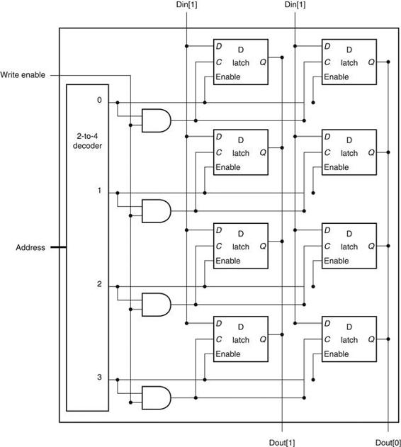
FIGURE B.9.3 The basic structure of a 4 × 2 SRAM consists of a decoder that selects which pair of cells to activate.
The activated cells use a three-state output connected to the vertical bit lines that supply the requested data. The address that selects the cell is sent on one of a set of horizontal address lines, called word lines. For simplicity, the Output enable and Chip select signals have been omitted, but they could easily be added with a few AND gates.
The design in Figure B.9.3 eliminates the need for an enormous multiplexor; however, it still requires a very large decoder and a correspondingly large number of word lines. For example, in a 4M × 8 SRAM, we would need a 22-to-4M decoder and 4M word lines (which are the lines used to enable the individual flip-flops)! To circumvent this problem, large memories are organized as rectangular arrays and use a two-step decoding process. Figure B.9.4 shows how a 4M × 8 SRAM might be organized internally using a two-step decode. As we will see, the two-level decoding process is quite important in understanding how DRAMs operate.
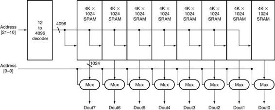
FIGURE B.9.4 Typical organization of a 4M × 8 SRAM as an array of 4K × 1024 arrays.
The first decoder generates the addresses for eight 4K × 1024 arrays; then a set of multiplexors is used to select 1 bit from each 1024-bit-wide array. This is a much easier design than a single-level decode that would need either an enormous decoder or a gigantic multiplexor. In practice, a modern SRAM of this size would probably use an even larger number of blocks, each somewhat smaller.
Recently we have seen the development of both synchronous SRAMs (SSRAMs) and synchronous DRAMs (SDRAMs). The key capability provided by synchronous RAMs is the ability to transfer a burst of data from a series of sequential addresses within an array or row. The burst is defined by a starting address, supplied in the usual fashion, and a burst length. The speed advantage of synchronous RAMs comes from the ability to transfer the bits in the burst without having to specify additional address bits. Instead, a clock is used to transfer the successive bits in the burst. The elimination of the need to specify the address for the transfers within the burst significantly improves the rate for transferring the block of data. Because of this capability, synchronous SRAMs and DRAMs are rapidly becoming the RAMs of choice for building memory systems in computers. We discuss the use of synchronous DRAMs in a memory system in more detail in the next section and in Chapter 5.
DRAMs
In a static RAM (SRAM), the value stored in a cell is kept on a pair of inverting gates, and as long as power is applied, the value can be kept indefinitely. In a dynamic RAM (DRAM), the value kept in a cell is stored as a charge in a capacitor. A single transistor is then used to access this stored charge, either to read the value or to overwrite the charge stored there. Because DRAMs use only a single transistor per bit of storage, they are much denser and cheaper per bit. By comparison, SRAMs require four to six transistors per bit. Because DRAMs store the charge on a capacitor, it cannot be kept indefinitely and must periodically be refreshed. That is why this memory structure is called dynamic, as opposed to the static storage in an SRAM cell.
To refresh the cell, we merely read its contents and write it back. The charge can be kept for several milliseconds, which might correspond to close to a million clock cycles. Today, single-chip memory controllers often handle the refresh function independently of the processor. If every bit had to be read out of the DRAM and then written back individually, with large DRAMs containing multiple megabytes, we would constantly be refreshing the DRAM, leaving no time for accessing it. Fortunately, DRAMs also use a two-level decoding structure, and this allows us to refresh an entire row (which shares a word line) with a read cycle followed immediately by a write cycle. Typically, refresh operations consume 1% to 2% of the active cycles of the DRAM, leaving the remaining 98% to 99% of the cycles available for reading and writing data.
Elaboration
How does a DRAM read and write the signal stored in a cell? The transistor inside the cell is a switch, called a pass transistor, that allows the value stored on the capacitor to be accessed for either reading or writing. Figure B.9.5 shows how the single-transistor cell looks. The pass transistor acts like a switch: when the signal on the word line is asserted, the switch is closed, connecting the capacitor to the bit line. If the operation is a write, then the value to be written is placed on the bit line. If the value is a 1, the capacitor will be charged. If the value is a 0, then the capacitor will be discharged. Reading is slightly more complex, since the DRAM must detect a very small charge stored in the capacitor. Before activating the word line for a read, the bit line is charged to the voltage that is halfway between the low and high voltage. Then, by activating the word line, the charge on the capacitor is read out onto the bit line. This causes the bit line to move slightly toward the high or low direction, and this change is detected with a sense amplifier, which can detect small changes in voltage.
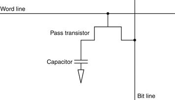
FIGURE B.9.5 A single-transistor DRAM cell contains a capacitor that stores the cell contents and a transistor used to access the cell.
DRAMs use a two-level decoder consisting of a row access followed by a column access, as shown in Figure B.9.6. The row access chooses one of a number of rows and activates the corresponding word line. The contents of all the columns in the active row are then stored in a set of latches. The column access then selects the data from the column latches. To save pins and reduce the package cost, the same address lines are used for both the row and column address; a pair of signals called RAS (Row Access Strobe) and CAS (Column Access Strobe) are used to signal the DRAM that either a row or column address is being supplied. Refresh is performed by simply reading the columns into the column latches and then writing the same values back. Thus, an entire row is refreshed in one cycle. The two-level addressing scheme, combined with the internal circuitry, make DRAM access times much longer (by a factor of 5–10) than SRAM access times. In 2004, typical DRAM access times ranged from 45 to 65 ns; 256 Mbit DRAMs are in full production, and the first customer samples of 1 GB DRAMs became available in the first quarter of 2004. The much lower cost per bit makes DRAM the choice for main memory, while the faster access time makes SRAM the choice for caches.
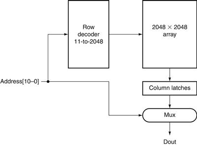
FIGURE B.9.6 A 4M × 1 DRAM is built with a 2048 × 2048 array.
The row access uses 11 bits to select a row, which is then latched in 2048 1-bit latches. A multiplexor chooses the output bit from these 2048 latches. The RAS and CAS signals control whether the address lines are sent to the row decoder or column multiplexor.
You might observe that a 64M × 4 DRAM actually accesses 8K bits on every row access and then throws away all but 4 of those during a column access. DRAM designers have used the internal structure of the DRAM as a way to provide higher bandwidth out of a DRAM. This is done by allowing the column address to change without changing the row address, resulting in an access to other bits in the column latches. To make this process faster and more precise, the address inputs were clocked, leading to the dominant form of DRAM in use today: syn chronous DRAM or SDRAM.
Since about 1999, SDRAMs are the memory chip of choice for most cache-based main memory systems. SDRAMs provide fast access to a series of bits within a row by sequentially transferring all the bits in a burst under the control of a clock signal. In 2004, DDRRAMs (Double Data Rate RAMs), which are called double data rate because they transfer data on both the rising and falling edge of an externally supplied clock, were the most heavily used form of SDRAMs. As we discuss in Chapter 5, these high-speed transfers can be used to boost the band width available out of main memory to match the needs of the processor and caches.
Error Correction
Because of the potential for data corruption in large memories, most computer systems use some sort of error-checking code to detect possible corruption of data. One simple code that is heavily used is a parity code. In a parity code the number of 1s in a word is counted; the word has odd parity if the number of 1s is odd and even otherwise. When a word is written into memory, the parity bit is also written (1 for odd, 0 for even). Then, when the word is read out, the parity bit is read and checked. If the parity of the memory word and the stored parity bit do not match, an error has occurred.
A 1-bit parity scheme can detect at most 1 bit of error in a data item; if there are 2 bits of error, then a 1-bit parity scheme will not detect any errors, since the parity will match the data with two errors. (Actually, a 1-bit parity scheme can detect any odd number of errors; however, the probability of having three errors is much lower than the probability of having two, so, in practice, a 1-bit parity code is limited to detecting a single bit of error.) Of course, a parity code cannot tell which bit in a data item is in error.
A 1-bit parity scheme is an error detection code; there are also error correction codes (ECC) that will detect and allow correction of an error. For large main memories, many systems use a code that allows the detection of up to 2 bits of error and the correction of a single bit of error. These codes work by using more bits to encode the data; for example, the typical codes used for main memories require 7 or 8 bits for every 128 bits of data.
error detection code
A code that enables the detection of an error in data, but not the precise location and, hence, correction of the error.
Elaboration
A 1-bit parity code is a distance-2 code, which means that if we look at the data plus the parity bit, no 1-bit change is sufficient to generate another legal combination of the data plus parity. For example, if we change a bit in the data, the parity will be wrong, and vice versa. Of course, if we change 2 bits (any 2 data bits or 1 data bit and the parity bit), the parity will match the data and the error cannot be detected. Hence, there is a distance of two between legal combinations of parity and data.
To detect more than one error or correct an error, we need a distance-3 code, which has the property that any legal combination of the bits in the error correction code and the data have at least 3 bits differing from any other combination. Suppose we have such a code and we have one error in the data. In that case, the code plus data will be one bit away from a legal combination, and we can correct the data to that legal combination. If we have two errors, we can recognize that there is an error, but we cannot correct the errors. Let’s look at an example. Here are the data words and a distance-3 error correction code for a 4-bit data item.

To see how this works, let’s choose a data word, say, 0110, whose error correction code is 011. Here are the four 1-bit error possibilities for this data: 1110, 0010, 0100, and 0111. Now look at the data item with the same code (011), which is the entry with the value 0001. If the error correction decoder received one of the four pos sible data words with an error, it would have to choose between correcting to 0110 or 0001. While these four words with error have only one bit changed from the correct pat tern of 0110, they each have two bits that are different from the alternate correction of 0001. Hence, the error correction mechanism can easily choose to correct to 0110, since a single error is a much higher probability. To see that two errors can be detected, simply notice that all the combinations with two bits changed have a different code. The one reuse of the same code is with three bits different, but if we correct a 2-bit error, we will correct to the wrong value, since the decoder will assume that only a single error has occurred. If we want to correct 1-bit errors and detect, but not erroneously correct, 2-bit errors, we need a distance-4 code.
Although we distinguished between the code and data in our explanation, in truth, an error correction code treats the combination of code and data as a single word in a larger code (7 bits in this example). Thus, it deals with errors in the code bits in the same fashion as errors in the data bits.
While the above example requires n − 1 bits for n bits of data, the number of bits required grows slowly, so that for a distance-3 code, a 64-bit word needs 7 bits and a 128-bit word needs 8. This type of code is called a Hamming code, after R. Hamming, who described a method for creating such codes.
B.10 Finite-State Machines
As we saw earlier, digital logic systems can be classified as combinational or sequential. Sequential systems contain state stored in memory elements internal to the system. Their behavior depends both on the set of inputs supplied and on the contents of the internal memory, or state of the system. Thus, a sequential sys tem cannot be described with a truth table. Instead, a sequential system is described as a finite-state machine (or often just state machine). A finite-state machine has a set of states and two functions, called the next-state function and the output function. The set of states corresponds to all the possible values of the internal storage. Thus, if there are n bits of storage, there are 2n states. The next-state function is a combinational function that, given the inputs and the current state, determines the next state of the system. The output function produces a set of outputs from the current state and the inputs. Figure B.10.1 shows this dia grammatically.
finite-state machine
A sequential logic function consisting of a set of inputs and out puts, a next-state function that maps the current state and the inputs to a new state, and an output function that maps the current state and possibly the inputs to a set of asserted outputs.
next-state function
A combinational function that, given the inputs and the current state, determines the next state of a finite-state machine.
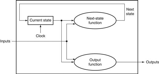
FIGURE B.10.1 A state machine consists of internal storage that contains the state and two combinational functions: the next-state function and the output function.
Often, the output function is restricted to take only the current state as its input; this does not change the capability of a sequential machine, but does affect its internals.
The state machines we discuss here and in Chapter 4 are synchronous. This means that the state changes together with the clock cycle, and a new state is computed once every clock. Thus, the state elements are updated only on the clock edge. We use this methodology in this section and throughout Chapter 4, and we do not usually show the clock explicitly. We use state machines throughout Chapter 4 to control the execution of the processor and the actions of the datapath.
To illustrate how a finite-state machine operates and is designed, let’s look at a simple and classic example: controlling a traffic light. (Chapters 4 and 5 contain more detailed examples of using finite-state machines to control processor execution.) When a finite-state machine is used as a controller, the output function is often restricted to depend on just the current state. Such a finite-state machine is called a Moore machine. This is the type of finite-state machine we use throughout this book. If the output function can depend on both the current state and the current input, the machine is called a Mealy machine. These two machines are equivalent in their capabilities, and one can be turned into the other mechanically. The basic advantage of a Moore machine is that it can be faster, while a Mealy machine may be smaller, since it may need fewer states than a Moore machine. In Chapter 5, we discuss the differences in more detail and show a Verilog version of finite-state control using a Mealy machine.
Our example concerns the control of a traffic light at an intersection of a north-south route and an east-west route. For simplicity, we will consider only the green and red lights; adding the yellow light is left for an exercise. We want the lights to cycle no faster than 30 seconds in each direction, so we will use a 0.033 Hz clock so that the machine cycles between states at no faster than once every 30 seconds. There are two output signals:
■ NSlite: When this signal is asserted, the light on the north-south road is green; when this signal is deasserted, the light on the north-south road is red.
■ EWlite: When this signal is asserted, the light on the east-west road is green; when this signal is deasserted, the light on the east-west road is red.
In addition, there are two inputs:
■ NScar: Indicates that a car is over the detector placed in the roadbed in front of the light on the north-south road (going north or south).
■ EWcar: Indicates that a car is over the detector placed in the roadbed in front of the light on the east-west road (going east or west).
The traffic light should change from one direction to the other only if a car is waiting to go in the other direction; otherwise, the light should continue to show green in the same direction as the last car that crossed the intersection.
To implement this simple traffic light we need two states:
■ NSgreen: The traffic light is green in the north-south direction.
■ EWgreen: The traffic light is green in the east-west direction.
We also need to create the next-state function, which can be specified with a table:
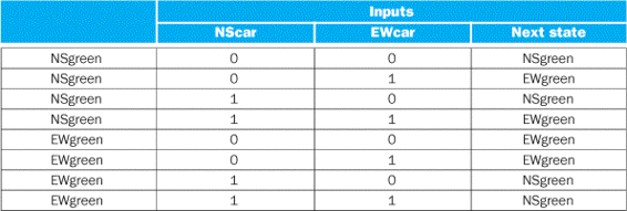
Notice that we didn’t specify in the algorithm what happens when a car approaches from both directions. In this case, the next-state function given above changes the state to ensure that a steady stream of cars from one direction cannot lock out a car in the other direction.
The finite-state machine is completed by specifying the output function.
Before we examine how to implement this finite-state machine, let’s look at a graphical representation, which is often used for finite-state machines. In this representation, nodes are used to indicate states. Inside the node we place a list of the outputs that are active for that state. Directed arcs are used to show the next-state

function, with labels on the arcs specifying the input condition as logic functions. Figure B.10.2 shows the graphical representation for this finite-state machine.
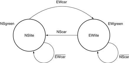
FIGURE B.10.2 The graphical representation of the two-state traffic light controller.
We simplified the logic functions on the state transitions. For example, the transition from NSgreen to EWgreen in the next-state table is ![]() , which is equivalent to EWcar.
, which is equivalent to EWcar.
A finite-state machine can be implemented with a register to hold the current state and a block of combinational logic that computes the next-state function and the output function. Figure B.10.3 shows how a finite-state machine with 4 bits of state, and thus up to 16 states, might look. To implement the finite-state machine in this way, we must first assign state numbers to the states. This process is called state assignment. For example, we could assign NSgreen to state 0 and EWgreen to state 1. The state register would contain a single bit. The next-state function would be given as
![]()
where Current State is the contents of the state register (0 or 1) and NextState is the output of the next-state function that will be written into the state register at the end of the clock cycle. The output function is also simple:
![]()
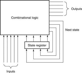
FIGURE B.10.3 A finite-state machine is implemented with a state register that holds the current state and a combinational logic block to compute the next state and output functions.
The latter two functions are often split apart and implemented with two separate blocks of logic, which may require fewer gates.
The combinational logic block is often implemented using structured logic, such as a PLA. A PLA can be constructed automatically from the next-state and output function tables. In fact, there are computer-aided design (CAD) programs that take either a graphical or textual representation of a finite-state machine and produce an optimized implementation automatically. In Chapters 4 and 5, finite-state machines were used to control processor execution. Appendix C discusses the detailed implementation of these controllers with both PLAs and ROMs.
To show how we might write the control in Verilog, Figure B.10.4 shows a Verilog version designed for synthesis. Note that for this simple control function, a Mealy machine is not useful, but this style of specification is used in Chapter 5 to implement a control function that is a Mealy machine and has fewer states than the Moore machine controller.
Check Yourself
What is the smallest number of states in a Moore machine for which a Mealy machine could have fewer states?
a. Two, since there could be a one-state Mealy machine that might do the same thing.
b. Three, since there could be a simple Moore machine that went to one of two different states and always returned to the original state after that. For such a simple machine, a two-state Mealy machine is possible.
c. You need at least four states to exploit the advantages of a Mealy machine over a Moore machine.
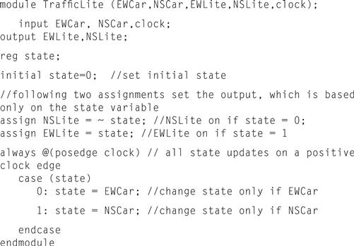
FIGURE B.10.4 A Verilog version of the traffic light controller.
B.11 Timing Methodologies
Throughout this appendix and in the rest of the text, we use an edge-triggered timing methodology. This timing methodology has an advantage in that it is simpler to explain and understand than a level-triggered methodology. In this section, we explain this timing methodology in a little more detail and also introduce level-sensitive clocking. We conclude this section by briefly discussing the issue of asynchronous signals and synchronizers, an important problem for digital designers.
The purpose of this section is to introduce the major concepts in clocking methodology. The section makes some important simplifying assumptions; if you are interested in understanding timing methodology in more detail, consult one of the references listed at the end of this appendix.
We use an edge-triggered timing methodology because it is simpler to explain and has fewer rules required for correctness. In particular, if we assume that all clocks arrive at the same time, we are guaranteed that a system with edge-triggered registers between blocks of combinational logic can operate correctly without races if we simply make the clock long enough. A race occurs when the contents of a state element depend on the relative speed of different logic elements. In an edge-triggered design, the clock cycle must be long enough to accommodate the path from one flip-flop through the combinational logic to another flip-flop where it must satisfy the setup-time requirement. Figure B.11.1 shows this requirement for a system using rising edge-triggered flip-flops. In such a system the clock period (or cycle time) must be at least as large as
![]()
for the worst-case values of these three delays, which are defined as follows:
■ tprop is the time for a signal to propagate through a flip-flop; it is also sometimes called clock-to-Q.
■ tcombinational is the longest delay for any combinational logic (which by definition is surrounded by two flip-flops).
■ tsetup is the time before the rising clock edge that the input to a flip-flop must be valid.

FIGURE B.11.1 In an edge-triggered design, the clock must be long enough to allow signals to be valid for the required setup time before the next clock edge.
The time for a flip-flop input to propagate to the flip-flip outputs is tprop; the signal then takes tcombinational to travel through the combinational logic and must be valid tsetup before the next clock edge.
We make one simplifying assumption: the hold-time requirements are satisfied, which is almost never an issue with modern logic.
One additional complication that must be considered in edge-triggered designs is clock skew. Clock skew is the difference in absolute time between when two state elements see a clock edge. Clock skew arises because the clock signal will often use two different paths, with slightly different delays, to reach two different state elements. If the clock skew is large enough, it may be possible for a state element to change and cause the input to another flip-flop to change before the clock edge is seen by the second flip-flop.
clock skew
The difference in absolute time between the times when two state elements see a clock edge.
Figure B.11.2 illustrates this problem, ignoring setup time and flip-flop propagation delay. To avoid incorrect operation, the clock period is increased to allow for the maximum clock skew. Thus, the clock period must be longer than
![]()

FIGURE B.11.2 Illustration of how clock skew can cause a race, leading to incorrect operation.
Because of the difference in when the two flip-flops see the clock, the signal that is stored into the first flip-flop can race forward and change the input to the second flip-flop before the clock arrives at the second flip-flop.
With this constraint on the clock period, the two clocks can also arrive in the opposite order, with the second clock arriving tskew earlier, and the circuit will work correctly. Designers reduce clock-skew problems by carefully routing the clock signal to minimize the difference in arrival times. In addition, smart designers also provide some margin by making the clock a little longer than the mini mum; this allows for variation in components as well as in the power supply. Since clock skew can also affect the hold-time requirements, minimizing the size of the clock skew is important.
Edge-triggered designs have two drawbacks: they require extra logic and they may sometimes be slower. Just looking at the D flip-flop versus the level-sensitive latch that we used to construct the flip-flop shows that edge-triggered design requires more logic. An alternative is to use level-sensitive clocking. Because state changes in a level-sensitive methodology are not instantaneous, a level-sensitive scheme is slightly more complex and requires additional care to make it operate correctly.
level-sensitive clocking
A timing methodology in which state changes occur at either high or low clock levels but are not instantaneous, as such changes are in edge-triggered designs.
Level-Sensitive Timing
In level-sensitive timing, the state changes occur at either high or low levels, but they are not instantaneous as they are in an edge-triggered methodology. Because of the noninstantaneous change in state, races can easily occur. To ensure that a level-sensitive design will also work correctly if the clock is slow enough, designers use two-phase clocking. Two-phase clocking is a scheme that makes use of two nonoverlapping clock signals. Since the two clocks, typically called Φ1 and Φ2, are nonoverlapping, at most one of the clock signals is high at any given time, as Figure B.11.3 shows. We can use these two clocks to build a system that contains level-sensitive latches but is free from any race conditions, just as the edge-triggered designs were.

FIGURE B.11.3 A two-phase clocking scheme showing the cycle of each clock and the nonoverlapping periods.
One simple way to design such a system is to alternate the use of latches that are open on Φ1 with latches that are open on Φ2. Because both clocks are not asserted at the same time, a race cannot occur. If the input to a combinational block is a Φ1 clock, then its output is latched by a Φ2 clock, which is open only during Φ2 when the input latch is closed and hence has a valid output. Figure B.11.4 shows how a system with two-phase timing and alternating latches operates. As in an edge-triggered design, we must pay attention to clock skew, particularly between the two clock phases. By increasing the amount of nonoverlap between the two phases, we can reduce the potential margin of error. Thus, the system is guaranteed to operate correctly if each phase is long enough and if there is large enough nonoverlap between the phases.

FIGURE B.11.4 A two-phase timing scheme with alternating latches showing how the system operates on both clock phases.
The output of a latch is stable on the opposite phase from its C input. Thus, the first block of combinational inputs has a stable input during ϕ2, and its output is latched by ϕ2. The second (rightmost) combinational block operates in just the opposite fashion, with stable inputs during ϕ1. Thus, the delays through the combinational blocks determine the minimum time that the respective clocks must be asserted. The size of the nonoverlapping period is determined by the maximum clock skew and the minimum delay of any logic block.
Asynchronous Inputs and Synchronizers
By using a single clock or a two-phase clock, we can eliminate race conditions if clock-skew problems are avoided. Unfortunately, it is impractical to make an entire system function with a single clock and still keep the clock skew small. While the CPU may use a single clock, I/O devices will probably have their own clock. Chapter 6 described how an asynchronous device may communicate with the CPU through a series of handshaking steps. To translate the asynchronous input to a synchronous signal that can be used to change the state of a system, we need to use a synchronizer, whose inputs are the asynchronous signal and a clock and whose output is a signal synchronous with the input clock.
metastability
A situation that occurs if a signal is sampled when it is not stable for the required setup and hold times, possibly causing the sampled value to fall in the indeterminate region between a high and low value.
Our first attempt to build a synchronizer uses an edge-triggered D flip-flop, whose D input is the asynchronous signal, as Figure B.11.5 shows. Because we communicate with a handshaking protocol (as we saw in Chapter 6), it does not matter whether we detect the asserted state of the asynchronous signal on one clock or the next, since the signal will be held asserted until it is acknowledged. Thus, you might think that this simple structure is enough to sample the signal accurately, which would be the case except for one small problem.

FIGURE B.11.5 A synchronizer built from a D flip-flop is used to sample an asynchronous signal to produce an output that is synchronous with the clock.
This “synchronizer” will not work properly!
The problem is a situation called metastability. Suppose the asynchronous signal is transitioning between high and low when the clock edge arrives. Clearly, it is not possible to know whether the signal will be latched as high or low. That problem we could live with. Unfortunately, the situation is worse: when the signal that is sampled is not stable for the required setup and hold times, the flip-flop may go into a metastable state. In such a state, the output will not have a legitimate high or low value, but will be in the indeterminate region between them. Furthermore, the flip-flop is not guaranteed to exit this state in any bounded amount of time. Some logic blocks that look at the output of the flip-flop may see its output as 0, while others may see it as 1. This situation is called a synchronizer failure.
synchronizer failure
A situation in which a flip-flop enters a metastable state and where some logic blocks reading the output of the flip-flop see a 0 while others see a 1.
In a purely synchronous system, synchronizer failure can be avoided by ensuring that the setup and hold times for a flip-flop or latch are always met, but this is impossible when the input is asynchronous. Instead, the only solution possible is to wait long enough before looking at the output of the flip-flop to ensure that its output is stable, and that it has exited the metastable state, if it ever entered it. How long is long enough? Well, the probability that the flip-flop will stay in the metastable state decreases exponentially, so after a very short time the probability that the flip-flop is in the metastable state is very low; however, the probability never reaches 0! So designers wait long enough that the probability of a synchronizer failure is very low, and the time between such failures will be years or even thousands of years.
For most flip-flop designs, waiting for a period that is several times longer than the setup time makes the probability of synchronization failure very low. If the clock rate is longer than the potential metastability period (which is likely), then a safe synchronizer can be built with two D flip-flops, as Figure B.11.6 shows. If you are interested in reading more about these problems, look into the references.
Check Yourself
Suppose we have a design with very large clock skew—longer than the register propagation time. Is it always possible for such a design to slow the clock down enough to guarantee that the logic operates properly?
a. Yes, if the clock is slow enough the signals can always propagate and the design will work, even if the skew is very large.
b. No, since it is possible that two registers see the same clock edge far enough apart that a register is triggered, and its outputs propagated and seen by a second register with the same clock edge.
propagation time
The time required for an input to a flip-flop to propagate to the outputs of the flip-flop.

FIGURE B.11.6 This synchronizer will work correctly if the period of metastability that we wish to guard against is less than the clock period.
Although the output of the first flip-flop may be metastable, it will not be seen by any other logic element until the second clock, when the second D flip-flop samples the signal, which by that time should no longer be in a metastable state.
B.12 Field Programmable Devices
Within a custom or semicustom chip, designers can make use of the flexibility of the underlying structure to easily implement combinational or sequential logic. How can a designer who does not want to use a custom or semicustom IC implement a complex piece of logic taking advantage of the very high levels of integra tion available? The most popular component used for sequential and combinational logic design outside of a custom or semicustom IC is a field programmable device (FPD). An FPD is an integrated circuit containing combina tional logic, and possibly memory devices, that are configurable by the end user.
field programmable devices (FPD)
An integrated circuit containing combinational logic, and possibly memory devices, that are configurable by the end user.
FPDs generally fall into two camps: programmable logic devices (PLDs), which are purely combinational, and field programmable gate arrays (FPGAs), which provide both combinational logic and flip-flops. PLDs consist of two forms: simple PLDs (SPLDs), which are usually either a PLA or a programmable array logic (PAL), and complex PLDs, which allow more than one logic block as well as configurable interconnections among blocks. When we speak of a PLA in a PLD, we mean a PLA with user programmable and-plane and or-plane. A PAL is like a PLA, except that the or-plane is fixed.
programmable logic device (PLD)
An integrated circuit containing combinational logic whose function is configured by the end user.
field programmable gate array (FPGA)
A configurable integrated circuit containing both combinational logic blocks and flip-flops.
simple programmable logic device (SPLD)
Programmable logic device, usually containing either a single PAL or PLA.
programmable array logic (PAL)
Contains a programmable and-plane followed by a fixed or-plane.
Before we discuss FPGAs, it is useful to talk about how FPDs are configured. Configuration is essentially a question of where to make or break connections. Gate and register structures are static, but the connections can be configured. Notice that by configuring the connections, a user determines what logic functions are implemented. Consider a configurable PLA: by determining where the connections are in the and-plane and the or-plane, the user dictates what logical functions are computed in the PLA. Connections in FPDs are either permanent or reconfigurable. Permanent connections involve the creation or destruction of a connection between two wires. Current FPLDs all use an antifuse technology, which allows a connection to be built at programming time that is then permanent. The other way to configure CMOS FPLDs is through an SRAM. The SRAM is downloaded at power-on, and the contents control the setting of switches, which in turn determines which metal lines are connected. The use of SRAM control has the advantage in that the FPD can be reconfigured by changing the contents of the SRAM. The disadvantages of the SRAM-based control are two: the configuration is volatile and must be reloaded on power-on, and the use of active transistors for switches slightly increases the resistance of such connections.
antifuse
A structure in an integrated circuit that when programmed makes a permanent connection between two wires.
FPGAs include both logic and memory devices, usually structured in a two-dimensional array with the corridors dividing the rows and columns used for global interconnect between the cells of the array. Each cell is a combination of gates and flip-flops that can be programmed to perform some specific function. Because they are basically small, programmable RAMs, they are also called lookup tables (LUTs). Newer FPGAs contain more sophisticated building blocks such as pieces of adders and RAM blocks that can be used to build register files. A few large FPGAs even contain 32-bit RISC cores!
In addition to programming each cell to perform a specific function, the interconnections between cells are also programmable, allowing modern FPGAs with hundreds of blocks and hundreds of thousands of gates to be used for complex logic functions. Interconnect is a major challenge in custom chips, and this is even more true for FPGAs, because cells do not represent natural units of decomposition for structured design. In many FPGAs, 90% of the area is reserved for interconnect and only 10% is for logic and memory blocks.
lookup tables (LUTs)
In a field programmable device, the name given to the cells because they consist of a small amount of logic and RAM.
Just as you cannot design a custom or semicustom chip without CAD tools, you also need them for FPDs. Logic synthesis tools have been developed that target FPGAs, allowing the generation of a system using FPGAs from structural and behavioral Verilog.
B.13 Concluding Remarks
This appendix introduces the basics of logic design. If you have digested the material in this appendix, you are ready to tackle the material in Chapters 4 and 5, both of which use the concepts discussed in this appendix extensively.
B.14 Exercises
B.1 [10] <§B.2> In addition to the basic laws we discussed in this section, there are two important theorems, called DeMorgan’s theorems:
![]()
Prove DeMorgan’s theorems with a truth table of the form

B.2 [15] <§B.2> Prove that the two equations for E in the example starting on page B-7 are equivalent by using DeMorgan’s theorems and the axioms shown on page B-7.
B.3 [10] <§B.2> Show that there are 2n entries in a truth table for a function with n inputs.
B.4 [10] <§B.2> One logic function that is used for a variety of purposes (including within adders and to compute parity) is exclusive OR. The output of a two-input exclusive OR function is true only if exactly one of the inputs is true. Show the truth table for a two-input exclusive OR function and implement this function using AND gates, OR gates, and inverters.
B.5 [15] <§B.2> Prove that the NOR gate is universal by showing how to build the AND, OR, and NOT functions using a two-input NOR gate.
B.6 [15] <§B.2> Prove that the NAND gate is universal by showing how to build the AND, OR, and NOT functions using a two-input NAND gate.
B.7 [10] <§§B.2, B.3> Construct the truth table for a four-input odd-parity function (see page B-65 for a description of parity).
B.8 [10] <§§B.2, B.3> Implement the four-input odd-parity function with AND and OR gates using bubbled inputs and outputs.
B.9 [10] <§§B.2, B.3> Implement the four-input odd-parity function with a PLA.
B.10 [15] <§§B.2, B.3> Prove that a two-input multiplexor is also universal by showing how to build the NAND (or NOR) gate using a multiplexor.
B.11 [5] <§§4.2, B.2, B.3> Assume that X consists of 3 bits, x2 x1 x0. Write four logic functions that are true if and only if
■ X contains only one 0
■ X contains an even number of 0s
■ X when interpreted as an unsigned binary number is less than 4
■ X when interpreted as a signed (two’s complement) number is negative
B.12 [5] <§§4.2, B.2, B.3> Implement the four functions described in Exercise B.11 using a PLA.
B.13 [5] <§§4.2, B.2, B.3> Assume that X consists of 3 bits, x2 x1 x0, and Y consists of 3 bits, y2 y1 y0. Write logic functions that are true if and only if
■ X , Y, where X and Y are thought of as unsigned binary numbers
■ X , Y, where X and Y are thought of as signed (two’s complement) numbers
■ X = Y
Use a hierarchical approach that can be extended to larger numbers of bits. Show how can you extend it to 6-bit comparison.
B.14 [5] <§§B.2, B.3> Implement a switching network that has two data inputs (A and B), two data outputs (C and D), and a control input (S). If S equals 1, the network is in pass-through mode, and C should equal A, and D should equal B. If S equals 0, the network is in crossing mode, and C should equal B, and D should equal A.
B.15 [15] <§§B.2, B.3> Derive the product-of-sums representation for E shown on page B-11 starting with the sum-of-products representation. You will need to use DeMorgan’s theorems.
B.16 [30] <§§B.2, B.3> Give an algorithm for constructing the sum-of-products representation for an arbitrary logic equation consisting of AND, OR, and NOT. The algorithm should be recursive and should not construct the truth table in the process.
B.17 [5] <§§B.2, B.3> Show a truth table for a multiplexor (inputs A, B, and S; output C ), using don’t cares to simplify the table where possible.
B.18 [5] <§B.3> What is the function implemented by the following Verilog modules:
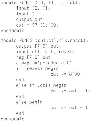
B.19 [5] <§B.4> The Verilog code on page B-53 is for a D flip-flop. Show the Verilog code for a D latch.
B.20 [10] <§§ B.3, B.4> Write down a Verilog module implementation of a 2-to-4 decoder (and/or encoder).
B.21 [10] <§§B.3, B.4> Given the following logic diagram for an accumulator, write down the Verilog module implementation of it. Assume a positive edge-triggered register and asynchronous Rst.
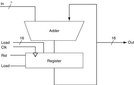
B.22 [20] <§§C3, B.4, B.5> Section 3.3 presents basic operation and possible implementations of multipliers. A basic unit of such implementations is a shift-and-add unit. Show a Verilog implementation for this unit. Show how can you use this unit to build a 32-bit multiplier.
B.23 [20] <§§C3, B.4, B.5> Repeat Exercise B.22, but for an unsigned divider rather than a multiplier.
B.24 [15] <§B.5> The ALU supported set on less than (slt) using just the sign bit of the adder. Let’s try a set on less than operation using the values −7ten and 6ten. To make it simpler to follow the example, let’s limit the binary representations to 4 bits: 1001two and 0110two.
1001two − 0110two = 1001two + 1010two = 0011two
This result would suggest that −7 > 6, which is clearly wrong. Hence, we must factor in overflow in the decision. Modify the 1-bit ALU in Figure B.5.10 on page B-33 to handle slt correctly. Make your changes on a photocopy of this figure to save time.
B.25 [20] <§B.6> A simple check for overflow during addition is to see if the CarryIn to the most significant bit is not the same as the CarryOut of the most significant bit. Prove that this check is the same as in Figure 3.2.
B.26 [5] <§B.6> Rewrite the equations on page B-44 for a carry-lookahead logic for a 16-bit adder using a new notation. First, use the names for the CarryIn signals of the individual bits of the adder. That is, use c4, c8, c12, … instead of C1, C2, C3, …. In addition, let Pi,j; mean a propagate signal for bits i to j, and Gi,j; mean a generate signal for bits i to j. For example, the equation
![]()
can be rewritten as
![]()
This more general notation is useful in creating wider adders.
B.27 [15] <§B.6> Write the equations for the carry-lookahead logic for a 64-bit adder using the new notation from Exercise B.26 and using 16-bit adders as building blocks. Include a drawing similar to Figure B.6.3 in your solution.
B.28 [10] <§B.6> Now calculate the relative performance of adders. Assume that hardware corresponding to any equation containing only OR or AND terms, such as the equations for pi and gi on page B-40, takes one time unit T. Equations that consist of the OR of several AND terms, such as the equations for c1, c2, c3, and c4 on page B-40, would thus take two time units, 2T. The reason is it would take T to produce the AND terms and then an additional T to produce the result of the OR. Calculate the numbers and performance ratio for 4-bit adders for both ripple carry and carry lookahead. If the terms in equations are further defined by other equations, then add the appropriate delays for those intermediate equations, and continue recursively until the actual input bits of the adder are used in an equation. Include a drawing of each adder labeled with the calculated delays and the path of the worst-case delay highlighted.
B.29 [15] <§B.6> This exercise is similar to Exercise B.28, but this time calculate the relative speeds of a 16-bit adder using ripple carry only, ripple carry of 4-bit groups that use carry lookahead, and the carry-lookahead scheme on page B-39.
B.30 [15] <§B.6> This exercise is similar to Exercises B.28 and B.29, but this time calculate the relative speeds of a 64-bit adder using ripple carry only, ripple carry of 4-bit groups that use carry lookahead, ripple carry of 16-bit groups that use carry lookahead, and the carry-lookahead scheme from Exercise B.27.
B.31 [10] <§B.6> Instead of thinking of an adder as a device that adds two numbers and then links the carries together, we can think of the adder as a hardware device that can add three inputs together (ai, bi, ci) and produce two outputs (s, ci + 1). When adding two numbers together, there is little we can do with this observation. When we are adding more than two operands, it is possible to reduce the cost of the carry. The idea is to form two independent sums, called S′ (sum bits) and C′ (carry bits). At the end of the process, we need to add C′ and S′ together using a normal adder. This technique of delaying carry propagation until the end of a sum of numbers is called carry save addition. The block drawing on the lower right of Figure B.14.1 shows the organization, with two levels of carry save adders connected by a single normal adder.
Calculate the delays to add four 16-bit numbers using full carry-lookahead adders versus carry save with a carry-lookahead adder forming the final sum. (The time unit T in Exercise B.28 is the same.)
B.32 [20] <§B.6> Perhaps the most likely case of adding many numbers at once in a computer would be when trying to multiply more quickly by using many adders to add many numbers in a single clock cycle. Compared to the multiply algorithm in Chapter 3, a carry save scheme with many adders could multiply more than 10 times faster. This exercise estimates the cost and speed of a combinational multiplier to multiply two positive 16-bit numbers. Assume that you have 16 intermediate terms M15, M14, …, M0, called partial products, that contain the multiplicand ANDed with multiplier bits m15, m14, …, m0. The idea is to use carry save adders to reduce the n operands into 2n/3 in parallel groups of three, and do this repeatedly until you get two large numbers to add together with a traditional adder.
First, show the block organization of the 16-bit carry save adders to add these 16 terms, as shown on the right in Figure B.14.1. Then calculate the delays to add these 16 numbers. Compare this time to the iterative multiplication scheme in Chapter 3 but only assume 16 iterations using a 16-bit adder that has full carry lookahead whose speed was calculated in Exercise B.29.
B.33 [10] <§B.6> There are times when we want to add a collection of numbers together. Suppose you wanted to add four 4-bit numbers (A, B, E, F) using 1-bit full adders. Let’s ignore carry lookahead for now. You would likely connect the 1-bit adders in the organization at the top of Figure B.14.1. Below the traditional organization is a novel organization of full adders. Try adding four numbers using both organizations to convince yourself that you get the same answer.
B.34 [5] <§B.6> First, show the block organization of the 16-bit carry save adders to add these 16 terms, as shown in Figure B.14.1. Assume that the time delay through each 1-bit adder is 2T. Calculate the time of adding four 4-bit numbers to the organization at the top versus the organization at the bottom of Figure B.14.1.
B.35 [5] <§B.8> Quite often, you would expect that given a timing diagram containing a description of changes that take place on a data input D and a clock input C (as in Figures B.8.3 and B.8.6 on pages B-52 and B-54, respectively), there would be differences between the output waveforms (Q) for a D latch and a D flip-flop. In a sentence or two, describe the circumstances (e.g., the nature of the inputs) for which there would not be any difference between the two output waveforms.
B.36 [5] <§B.8> Figure B.8.8 on page B-55 illustrates the implementation of the register file for the MIPS datapath. Pretend that a new register file is to be built, but that there are only two registers and only one read port, and that each register has only 2 bits of data. Redraw Figure B.8.8 so that every wire in your diagram corresponds to only 1 bit of data (unlike the diagram in Figure B.8.8, in which some wires are 5 bits and some wires are 32 bits). Redraw the registers using D flip-flops. You do not need to show how to implement a D flip-flop or a multiplexor.
B.37 [10] <§B.10> A friend would like you to build an “electronic eye” for use as a fake security device. The device consists of three lights lined up in a row, controlled by the outputs Left, Middle, and Right, which, if asserted, indicate that a light should be on. Only one light is on at a time, and the light “moves” from left to right and then from right to left, thus scaring away thieves who believe that the device is monitoring their activity. Draw the graphical representation for the finite-state machine used to specify the electronic eye. Note that the rate of the eye’s movement will be controlled by the clock speed (which should not be too great) and that there are essentially no inputs.
B.38 [10] <§B.10> {Ex. B.37} Assign state numbers to the states of the finite-state machine you constructed for Exercise B.37 and write a set of logic equations for each of the outputs, including the next-state bits.
B.39 [15] <§§B.2, B.8, B.10> Construct a 3-bit counter using three D flip-flops and a selection of gates. The inputs should consist of a signal that resets the counter to 0, called reset, and a signal to increment the counter, called inc. The outputs should be the value of the counter. When the counter has value 7 and is incremented, it should wrap around and become 0.
B.40 [20] <§B.10> A Gray code is a sequence of binary numbers with the property that no more than 1 bit changes in going from one element of the sequence to another. For example, here is a 3-bit binary Gray code: 000, 001, 011, 010, 110, 111, 101, and 100. Using three D flip-flops and a PLA, construct a 3-bit Gray code counter that has two inputs: reset, which sets the counter to 000, and inc, which makes the counter go to the next value in the sequence. Note that the code is cyclic, so that the value after 100 in the sequence is 000.
B.41 [25] <§B.10> We wish to add a yellow light to our traffic light example on page B-68. We will do this by changing the clock to run at 0.25 Hz (a 4-second clock cycle time), which is the duration of a yellow light. To prevent the green and red lights from cycling too fast, we add a 30-second timer. The timer has a single input, called TimerReset, which restarts the timer, and a single output, called TimerSignal, which indicates that the 30-second period has expired. Also, we must redefine the traffic signals to include yellow. We do this by defining two out put signals for each light: green and yellow. If the output NS green is asserted, the green light is on; if the output NSyellow is asserted, the yellow light is on. If both signals are off, the red light is on. Do not assert both the green and yellow signals at the same time, since American drivers will certainly be confused, even if European drivers understand what this means! Draw the graphical representation for the finite-state machine for this improved controller. Choose names for the states that are different from the names of the outputs.
B.42 [15] <§B.10> {Ex. B.41} Write down the next-state and output-function tables for the traffic light controller described in Exercise B.41.
B.43 [15] <§§B.2, B.10> {Ex. B.42} Assign state numbers to the states in the traffic light example of Exercise B.41 and use the tables of Exercise B.42 to write a set of logic equations for each of the outputs, including the next-state outputs.
B.44 [15] <§§B.3, B.10> {Ex. B.43} Implement the logic equations of Exercise B.43 as a PLA.
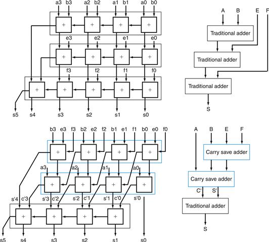
FIGURE B.14.1 Traditional ripple carry and carry save addition of four 4-bit numbers.
The details are shown on the left, with the individual signals in lowercase, and the corresponding higher-level blocks are on the right, with collective signals in upper case. Note that the sum of four n-bit numbers can
Answers to Check Yourself
§B.2, page B-8: No. If A = 1, C = 1, B = 0, the first is true, but the second is false.
§B.3, page B-20: C.
§B.4, page B-22: They are all exactly the same.
§B.4, page B-26: A = 0, B = 1.
§B.5, page B-38: 2.
§B.6, page B-47: 1.
§B.8, page B-58: c.
§B.10, page B-72: b.
§B.11, page B-77: b.
Further Reading
There are a number of good texts on logic design. Here are some you might like to look into.
1. Ciletti MD. Advanced Digital Design with the Verilog HDL Englewood Cliffs, NJ: Prentice Hall; 2002.
1a. A thorough book on logic design using Verilog.
2. Katz RH. Modern Logic Design 2nd ed. Reading, MA: Addison-Wesley; 2004.
2a. A general text on logic design.
3. Wakerly JF. Digital Design: Principles and Practices 3rd ed. Englewood Cliffs, NJ: Prentice Hall; 2000.
3a. A general text on logic design.