Professional Embedded ARM Development (2014)
Part I. ARM Systems and Development
Chapter 3. ARM Architecture
WHAT’S IN THIS CHAPTER?
Understanding the basic terms
Understanding a processor
ARM processor internals
Understanding program flow and interruption
The different technologies
It doesn’t matter if you are talking about an ARM processor, a 68k or even an x86 processor; they all have some common subsystems. There are slight differences in the way some subsystems are accessed, or the amount of subsystems present, but all processors retain the same basic principle, no matter what architecture. Following is a brief explanation of the core technology found in all modern processors, before going deeper into the specific details that make ARM processors what they are.
UNDERSTANDING THE BASICS
Everything in a computer is a number — text, images, sounds — everything is written down as a collection of numbers. A computer’s job is to take some data and run operations on it; put simply, take some numbers, and do some mathematical computations.
The Colossus was the first programmable digital electronic computer, used in Britain during World War II to help in the cryptanalysis of the Lorenz cipher code, a cryptocode used by the German High Command to communicate with its armies. Colossus didn’t actually completely decrypt messages; it was used to break Lorenz key settings using specialized code. Colossus could outperform humans both in terms of speed and reliability, and by the end of the war ten Colossus computers were in service.
While the Colossus was programmable, it was not a general purpose computer. It was designed with a specific task in mind and could not be programmed for another task, only programmed for different calculations on the same cipher. Programming was accomplished by setting up plugs and switches before reading in a cipher.
In America, the ENIAC was announced in 1946 and was used mainly to calculate ballistic trajectory, but was also used as a calculator for the hydrogen bomb project. What made it unique was its capacity of branching, or executing computer code depending on a previous result. Instead of a calculator simply adding numbers together, a computer could conditionally execute; take this number and multiply it by 2. Is the result less than 0? If it isn’t, then subtract 20; otherwise, add 10. For ballistics, a computer could be told to continue calculating the speed, distance, and height of the projectile and to continue as long as the height is above sea level.
To function, a computer needs several things:
A processor, on which all the work will be done
Memory, to store information
Input and output, to get information and to return it to the user (or activate outputs depending on certain conditions)
The processor is the ARM core. It might be an ARM Classic processor, such as an ARM11, or a Cortex, for example a Cortex-A8.
The memory might be more complicated. There are often several types of memory on an embedded system. There might be large amounts of DDR storage available, but DDR requires an initialization sequence, and therefore, memory. ARM systems often come with a small amount of internal memory (enough to start the system and to initialize any external systems) such as DDR memory, or possibly flash memory to read the operating system from.
Input and output can be almost anything and are either directly on the processor or SoC, or specific components mapped to external addresses.
Register
A CPU register is a small amount of fast memory that is built directly into the CPU and is used to manipulate data. ARM CPUs are load/store architecture, meaning that all calculation done on a CPU is done directly onto registers. First, the CPU reads from main memory into a register before making calculations, and possibly writing the value out into main memory. No instructions operate directly onto values in main memory. This might sound inefficient, but in practice it isn’t; it saves having to write to main memory after each operation. It also significantly simplifies the pipeline architecture, something that is crucial for RISC processors.
At first glance, it might be surprising that there are so few registers on a system, but with a bit of careful work, most routines can be created using few registers. ARM processors actually have more registers than some.
Stack
The stack is a memory location in which temporary data is put and retrieved when needed. It is a LIFO: Last In, First Out. Some card games use a stack; a place in which cards can be put and retrieved but only in a specific order; the last card placed is the first one out. To get to a specific card, you must first remove all the other cards above it. The stack works in the same way.
The stack is primarily used when executing subroutines. When entering a subroutine, care must be taken to ensure that some registers retain their initial value, and to do that, their contents are placed onto the stack. So long as care is taken to take back the same amount of elements as was put into the stack, then the same values will always be read back.
The stack can fill up quickly, depending on the situation. During complicated calculations, variables must be pushed onto the stack to make room for new data. When calling a subroutine with complex arguments, they are often pushed onto the stack, and in the case of an object, the entire object is pushed onto the stack. This can result in huge increases in the stack size, so care must be taken to ensure that the stack does not overflow.
Internal RAM
Not all processors have internal RAM, but most do. It is often small compared to system memory, but it serves its purpose. On a typical system, there might be as much as 512 megabytes of external DDR memory, but DDR memory takes time to initialize. You need to do lots of steps to get DDR memory up and running, and in the meantime you cannot do your job with registers alone. Therefore, most ARM processors have a minimal amount of internal RAM, where you can transfer a program and run it, therefore setting up critical systems before switching to DDR memory. Internal RAM is also usually much faster than external RAM.
Cache
Early CPUs read instructions directly from the system memory, but when considering the time it takes to read data from the system memory compared to a processor cycle time, it was clear that a large portion of the CPUs’ time was spent waiting for data to arrive. Writing data to the system memory was often even worse. Something had to be done, and so cache memory was developed.
CPU technology advancements mean that the speed of CPUs has grown many times in comparison to the access speed of main memory. If every instruction on a CPU required a memory access, the maximum speed of a CPU would be the maximum speed of the system memory. This problem is known as the memory bottleneck.
Cache memory is made from a special sort of memory, SRAM. SRAM, or Static RAM, has a speed advantage over DRAM, or Dynamic RAM. Unlike DRAM, SRAM does not need to be refreshed and can hold data indefinitely provided that it remains powered. SRAM provides high speed, but the cost is prohibitively high, so only a small amount of SRAM is available; main system memory is rarely SRAM.
Cache memory is used to store information recently accessed by a processor. Several layers of cache may be implemented: Cache (Level 1) is the closest to the CPU and the fastest. It is often relatively small, varying between 4 KB and 64 KB in size. L2 cache (Level 2) is often slightly slower than L1 but also much larger. L2 cache can be in the range of 128 KB all the way to 4 MB or more.
There are two distinct cache architectures: Von Neumann (or unified) and Harvard. Unified cache is a single memory cache used for all memory zones. Harvard cache separates instruction cache and data cache. The separate caches are often referred to as D-cache (data cache) and I-cache (instruction cache). Harvard architectures have physically separate signals for storage for code and data memory, and Von Neumann architectures have shared signals and memory for code and data.
On boot, caches are disabled but not necessarily invalidated; they must be specifically set up and configured to function.
Read Cache Strategy
Cache memory is designed to avoid lengthy reads and writes, by reading in sections of memory into cache upon first use in the hope that future reads can then read from cache. If the processor requests some data, it first checks the cache. If it finds the data available, it is called a cache hit, and the data will be available immediately without having to read data from external RAM. If the data is not available, it is a cache miss, and the relevant data must be read from the system memory into the cache. Instead of reading in a single value, a cache line is read in.
Although this can be useful for some portions of the system memory, there are locations in which you do not want cache to operate at all. Caching the serial port could be disastrous; instead of reading from the serial register, you would constantly be reading the cache and presuming that no data is available. That is where memory management comes in — you can program specific memory zones to be cacheable or non-cacheable.
Memory management is done by the Memory Management Unit (MMU) or, for some systems, the Memory Protection Unit (MPU). For some Cortex-M systems, neither MMU nor MPU is available, and the cacheable attributes or memory regions are part of the fixed architectural map.
Of course, using this strategy, you are soon presented with a problem. When a cache-miss is encountered and the cache is full, what happens? In this case, one of the cache entries has to be evicted, leaving place for a new entry. But which one? This is one of the subjects on optimization; the trick is to know which cache entries will be used in the future. Because it is extremely difficult to know what will be used and what won’t, one of the cache eviction strategies is LRU, or Least-Recently Used. By using this technique, the most recently accessed cache will remain, and older entries will be deleted. Careful planning can help optimize systems by defining which sections of memory are cacheable and which ones aren’t.
Write Cache Strategy
Write-cache strategy is comparable to read-cache strategy, but there is a difference. Writing to cache can effectively speed up operation, but sooner or later the external memory needs to be updated, and you must first think about how to do that. There are two possible policies: write-through and write-back.
When writing data with the write-through policy, data is written to the cache, and at the same time written to system memory. Subsequent reads will read from the cache. Write-back cache is slightly different from write-through. Initially, writing is done only to the cache; writing to external memory is postponed until the cache blocks are to be replaced or updated with new content. Cache lines that have been modified are marked as dirty. Write-back does have speed advantages but is more complex to implement and also has a drawback. A read miss in a write-back cache (requiring a block to be replaced by a data read) often requires two memory accesses: one to write the dirty cache line to system data and one to read system data into a new cache line.
GETTING TO KNOW THE DIFFERENT ARM SUBSYSTEMS
After having shown the basics, I will now show some of the subsystems on ARM processors. They are the components that make up an ARM processor, and are essential components to an ARM core.
Presenting the Processor Registers
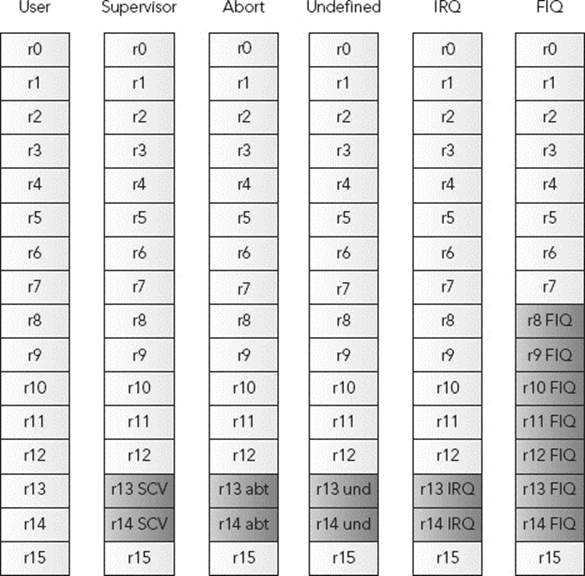
An ARM core can be thought of as having 16 32-bit general registers; named r0 to r15. In reality, however, there are several more because some registers are mode-specific. They are known as banked registers. Registers r0 to r7 are the same across all CPU modes; they are never banked. Registersr8 to r12 are the same across all CPU modes, except for FIQ. r13, r14, and r15 are unique to each mode and do not need to be saved.
As you can see in Figure 3-1, when switching from User Mode to Fast Interrupt Mode, you still have the same registers r0 to r7. That means that the values that were in r0 to r7 are still there, and when returning from Fast Interrupt, you return to where you were before the interrupt, and that portion of code expects to find the same values. However, r8 to r14 are “banked,” meaning that these registers are used only inside your current mode of operation. The original r8 to r14 are still there and will be visible after you exit the fast interrupt. The advantage of this is speed; on returning, the registers must be set to their original values.
FIGURE 3-1: ARM Registers in different modes
In normal programming, the user can freely access and write registers r0 to r12. r13, r14, and r15 are reserved for special purposes. The ARM coding conventions (the AAPCS, Procedure Call Standard for the ARM Architecture) state that when calling a subroutine, the arguments are passed in the first four registers (r0 to r3), and return values are also passed in r0 to r3. A subroutine must preserve the contents of the registers r4-r11. It is up to the subroutine to see if it necessary to push registers to the stack, or if it is possible to make required calculations on the first four registers. Whatever the decision, on returning, the caller function must have the result in r1, and the contents of r4 to r12 must be preserved.
r0 to r3
Normally, the first four registers, r0 to r3, are used to pass arguments to a function. After these four registers have been used, any further arguments must be placed onto the stack. This can be configured with a compiler option. r0 is also used as the return value of a function. If the return value is more than 32-bits wide, r1 is also used. A program must assume that any function call will corrupt r0 to r3.
r4 to r11
r4 to r11 are general purpose registers and can be used for any calculation, but they must be preserved by a function if their values are changed.
r12
r12 is sometimes known as the IP register and can be used as an interprocess scratch register. The exact use depends heavily on the system being used, and in some cases, it is used as a general purpose register. If you use an operating system, refer to the operating system guide as to the usage ofr12. If you are creating a bare metal system, you can use r12 as you see fit.
The AAPCS states that r12 may be corrupted by any function call, so programs must assume that it will not be preserved across a call.
r13: The Stack Pointer
The stack pointer is an important register. r13 has a special function; it is the stack pointer. Just like the other registers, it is possible to read and write to this register, but most dedicated instructions will change the stack pointer as required. It is necessary to set up this register by writing the correct address, but after that, it is no longer necessary to directly change this register. Thumb even forbids changing the stack pointer, with the exception of add and subtract.
When entering a function, r4 to r11 need to be returned to their initial values before leaving. To do that, use the PUSH and POP instructions, both of which modify the SP as required. Of course, it is not efficient to automatically PUSH and POP all the registers; therefore, the compiler will look and see what is to be done and will operate only on the registers that need to be saved, for example:
subroutine PUSH {r0-r3,r12,lr} ; Push working registers and the link register
BL my_function
; my_function will return here
POP {r0-r3,r12,pc} ; Pop working registers, r12 and the PC
r14: The Link Register
r14 holds the value of the Link Register, the memory address of an instruction to be run when a subroutine has been completed. Effectively, it contains the memory address to return to after you finish your task. When the processor encounters a branch with link instruction, a BL, r14 is loaded with the address of the next instruction. When the routine finishes, executing BX returns to where the program was.
Here is an example:
AREA subrout, CODE, READONLY ; Name this block of code
ENTRY ; Mark first instruction to execute
start MOV r0, #10 ; Set up parameters
MOV r1, #3
BL doadd ; Call subroutine
[ ... ]
doadd ADD r0, r0, r1 ; Subroutine code
BX lr; Return from subroutine
END ; Mark end of file
r15: The Program Counter
r15 holds the value of the Program Counter, the memory address of the next instruction to be fetched from memory. It is a read/write register; it can be written to, as is sometimes the case when returning from a branch instruction, modifying the address of the next instruction to be executed.
There is, however, a trick. Although technically the PC holds the address of the next instruction to be loaded, in reality it holds the location of the next instruction to be loaded into the pipeline, which is the address of the currently executing instruction plus two instructions. In ARM state, this is 8 bytes ahead, and in Thumb state it is 4 bytes. Most debuggers will hide this from you and show you the PC value as the address of the currently executing instruction, but some don’t. If, during your debugging session, the PC points to something that doesn’t seem related, check the documentation to see what the PC is supposed to show.
Presenting the CPSR
The CPSR is technically a register but not like the registers r0 to r15. The CPSR, short for Current Program Status Register, is a critical register that holds the status of the running program and is updated continuously. It contains condition code flags, which may be updated when an ALU operation occurs. Compare instructions automatically update the CPSR. Most other instructions do not automatically update the CPSR but can be forced to by adding the S directive after the instruction.
The ARM core uses the CPSR to monitor and control internal operations. The CPSR holds the following, among others:
Current processor mode
Interrupt disable flags
Current processor state (ARM, Thumb, Jazelle, and so on)
Data memory endianness (for ARMv6 and later)
Condition flags
CPSR specifications may vary slightly from one architecture to another as ARM implements new features.
If the CPSR is the Current PSR, the SPSR is the Saved PSR. When an ARM processor responds to an event that generates an exception, the CPSR is saved into the SPSR. Each mode can have its own CPSR, and when the exception has been handled, the SPSR is restored into the CPSR, and program execution can continue. This also has the advantage of returning the processor to its exact previous state.
Understanding Condition Flags
The ALU is connected directly to the CPSR and can update the CPSR registers directly depending on the result of a calculation (or comparison).
N – Negative
This bit is set if the result of a data processing instruction was negative.
Z – Zero
This bit is set if the result was zero.
C – Carry
This bit is set if the result of an operation was greater than 32 bits.
V – Overflow
This bit is set if the result of an operation was greater than 31 bits, indicating possible corruption of the signed bit in signed numbers.
In 2’s complement notation, the largest signed 32-bit number a register can hold is 0x7fffffff, so if you add 0x7fffffff and 0x7fffffff, you can generate an overflow because the result is larger than a signed 32-bit number, but the Carry (C) is not set because you do not overflow an unsigned 32-bit number.
Interrupt Masks
Interrupt masks are used to stop (or allow) specific interrupt requests from interrupting the processor. It is often useful to disable interrupts for specific tasks before re-enabling them. When servicing an IRQ, further IRQs are disabled and FIQs are not modified. When servicing a fast interrupt, FIQs and IRQs are disabled; that way, critical code cannot be interrupted. When the interrupt operation is over, the SPSR is restored and the processor is returned to its previous state (with the previous settings for interrupts).
On some cores, there is a special interrupt that cannot be disabled — NMI, or Non-maskable Interrupt.
Calculation Unit
The calculation unit, as shown in Figure 3-2, is the heart of an ARM processor.
FIGURE 3-2: ARM Calculation Unit
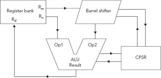
The Arithmetic Logic Unit (ALU) has two 32-bit inputs. The first comes directly from the register bank, and the second one comes from the shifter. The ALU is connected to the CPSR and can shape the calculation output depending on the CPSR contents and also update CPSR contents according to the results of a calculation. For example, if a mathematical operation overflows, the ALU can update the CPSR directly.
You must understand that ARM cores in ARM mode do not actually need shift instructions, contrary to many other processors. Instead, the barrel shifter can perform a shift during an instruction by specifying a shift on the second operator directly inside an instruction. In Thumb mode, the instructions are simplified and shift instructions do exist.
Pipeline
The pipeline is a technique used in the design of ARM processors (and others) to increase instruction throughput. Instead of having to fetch an instruction, decode the instruction, and then execute it, you can do all three at the same time but not on the same instruction.
Imagine a factory. Imagine a worker inside the factory making a family computer. He first gets the mainboard and puts it inside the chassis. Then he takes the processor and puts it on the mainboard. Then he installs the RAM, and finally, he installs the graphics card. One worker has made the entire computer; one person is responsible for the entire chain. That isn’t how they are made, though; computer manufacturers rely on assembly lines. One person will put the mainboard inside the chassis, and instead of continuing to the next task, he will repeat the process. The next worker on the assembly line will take the work of the first person and install the processor onto the mainboard, and again, the next task will be performed by someone else. The advantage is that each task is simplified, and the process can be greatly accelerated. Since each task is simple it can be easily duplicated, making several lines, parallelizing fabrication, and doubling the output.
Although making a desktop PC might seem relatively simple, imagine the complexity of a laptop computer, a flat-screen TV, or a car. Each task, although simple compared to the entire product, is still complex.
A CPU pipeline works in the same way. For example, one part of the processor constantly fetches the next instruction, another part “decodes” the instruction that has been fetched, and finally, another part executes that instruction. CPUs are driven by a clock; by doing more things on each clock pulse, you can increase the throughput of the CPU, and since each operation is made simpler, it becomes easier to increase the clock speed, further increasing throughput.
The advantage is, or course, speed. However, there are disadvantages of a pipelined system, notably stalls. A stall occurs when a pipeline cannot continue doing work as normal. For example, Figure 3-3 shows a typical six-stage pipeline.
FIGURE 3-3: ARM six stage pipeline

Stage 3 accesses any operands that may be required from the register bank. After the calculation is done, in stage 6, you can write the results back into the register bank. Now suppose you have this:
MOV r5, #20
MOV r8, [r9]
ADD r0, r1, r2
SUB r0, r0, r3
MOV r4, r6
MVN r7, r10
Each instruction is run sequentially. The first Move instruction moves the value 20 into r5. The second Move instruction requires a fetch from memory, and assuming that this data is not located in cache, it can take some time. However, the data will be written into r8, and the instructions behind it do not require r8, so they would be stalled, waiting for an instruction to finish without even requiring the result.
There are different techniques to avoid stalls. One of the main reasons for stalls are branches. When a branch occurs, the pipeline needs to be filled with new instructions, which are probably in a different memory location. Therefore, the processor needs to fetch a new memory location, place the first instruction at the beginning of the pipeline, and then begin working on the instruction. In the meantime, the “execution” phase has to wait for instructions to arrive. To avoid this, some ARM processors have branch prediction hardware, effectively “guessing” the outcome of a conditional jump. The branch predictor then fills in the pipeline with the predicted outcome. If it is correct, a stall is avoided because instructions are already present in the pipeline. Some branch predictors have been reported to be 95 percent correct. More recent branch predictors even manage a 100 percent mark by speculatively fetching both possible execution paths, and discarding one of them once the outcome of the branch is known.
There are several cases where the order of instructions can cause stalls. In the previous example, the result of a memory fetch wasn’t required, but what would happen if the instruction immediately afterwards required that result? Pipeline optimization would not be able to counter the stall, and the pipeline might stall for a significant amount of time. The answer to this is “instruction scheduling,” which rearranges the order of instructions to avoid stalls. If a memory fetch might stall a pipeline, a compiler may place the instruction earlier, thus giving the pipeline a little more time.
Another technique used on some processors is known as out-of-order execution. Instead of the compiler rearranging instructions, the ARM core can sometimes rearrange instructions itself.
Tightly Coupled Memory
Cache can greatly increase speed, but it also adds problems. Sometimes, you need data to be stored in memory that isn’t cacheable to be certain of the contents. Sometimes, you also want data to be “always available” and to have the speed of something in cache but without using up all the system cache. When reading data, if you have a cache hit, the data is immediately available, but if you have a cache miss, that data must be read from the system memory, often slowing down the system, in some cases considerably. You want critical interrupt handler code to be “always available,” interrupt stacks, or mathematical data if the calculations require vast amounts of raw data.
Tightly Coupled Memory (TCM) is available on some processors. When available, TCM exists in parallel to the L1 caches and is extremely fast (typically one or two cycles’ access time). The TCM is consequently not cacheable, leaving the cache free for other instructions and data.
TCM is like internal RAM, only configurable. By setting registers in the CP15, you can select separate instruction-side and data-side memory, either instruction or data-side memory, or complete deactivation of the TCM. It can be placed anywhere in the address map, as long as it is suitably aligned.
Coprocessors
ARM processors have an elegant way to extend their instruction set. ARM processors have support for coprocessors; secondary units that can handle instructions while the processor continues doing work.
The coprocessor space is divided into 16 coprocessors, numbered 0 to 15. Coprocessor 15 (CP15) is reserved for control functions, used mainly for managing caches and configuring the MMU. CP14 is reserved for debug, and CP 10 and 11 are reserved for NEON and VFP.
For classic processors, when a processor encounters an unknown instruction, it offers that instruction to any coprocessor present. Each coprocessor decodes the instruction to see if it can handle the instruction and signals back to the processor. If a coprocessor accepts the instruction, it takes the instruction and executes it using its own registers. If no coprocessor can handle the instruction, the processor initiates an undefined instruction exception. This is an elegant solution because some software enables “soft” coprocessors. If a coprocessor is not present, the instruction is caught during an exception and executed in software. Although the result is naturally slower than if the coprocessor was present, it does mean that the same code can be run, regardless of the availability of a specific coprocessor.
This system no longer exists; Cortex processors do not have a coprocessor interface, and instead, the instructions have been implemented into the core pipeline. Coprocessor instructions still exist and documents will still talk about the CP15 or other coprocessors; however, in order to simplify the core, the older coprocessor structure has been removed, but the instructions became valid ARM instructions. The coprocessor interface bus has 224 signals in it, so simplifying the coprocessor design was an important step to making processors simpler and faster.
CP15: The System Coprocessor
CP15 is a coprocessor interface developed by ARM and present on almost all processors except for the Cortex-M range.
The CP15’s role is to handle system configuration: data cache, tightly coupled memory, MMU/MPU, and system performance monitoring. They are configured using the MRC/MCR instructions and can be accessed only in privileged modes. The registers are processor-specific; refer to your manual for more detailed information.
CP14: The Debug Coprocessor
The CP14 provides status information about the state of the debug system, configuration of certain aspects of the debug system, vector catching, and breakpoint and watchpoint configuration.
UNDERSTANDING THE DIFFERENT CONCEPTS
Before using an ARM processor, you need to know a few concepts. These concepts are the basis of ARM systems; some are related to the embedded systems world; others are purely ARM.
What Is an Exception?
Microprocessors can respond to an asynchronous event with a context switch. Typically, an external hardware device activates a specific input line. A serial driver might create an interrupt to tell the CPU that data is ready to be read in, or maybe a timer that sends signals periodically. It is the hardware’s way of saying, “I have something I need done.” This makes the processor do something that is called a context switch; the processor stops what it was doing and responds to the interrupt. Imagine working at your desk, when the phone rings. This forces you into a context switch. You make a mental note of what you were doing, you acknowledge that the phone is ringing, and now you are free to choose what to do next. You could answer it, and what you were doing before has to wait. You could send the call to someone else or even ignore the call. Whatever you choose, you return to your previous task where you left off. For a processor, it is the same thing. When an interrupt arrives, you initiate a context switch. Registers can change, the current status is updated, and the current memory address is saved so that you can return later.
During its life cycle, a processor runs a program. Anything that disturbs that operation is called an exception. A software or hardware interrupt, a data abort, and an illegal instruction change the normal execution of a processor and are all exceptions. Even a reset is called an exception. When an exception occurs, the PC is placed onto the vector table at the corresponding entry, ready to execute a series of instructions before returning to what the processor was doing before (except for the reset exception). Several exceptions are available with different priorities.
Reset
A Reset exception has the highest priority because this is an external action that will put the processor in Reset state. When a CPU is powered on, it is considered to be in a Reset state. From here, you probably need to initialize all the hardware. When starting in Reset state, the core is in Supervisor mode, with all interrupts disabled.
Data Abort
A Data Abort happens when a data memory read or write fails. This can be for several reasons, but mostly it occurs when reading from or writing to an invalid address. When a Data Abort happens, the CPU is put into Abort mode, IRQ is disabled, FIQ remains unchanged, and r14 contains the address of the aborted instruction, plus 8.
IRQ Interrupt
An IRQ interrupt occurs when an external peripheral sets the IRQ pin. It is used for peripherals to indicate that they are awaiting service and need the CPU to do something. Some examples are an input device indicating that the user has entered data, a network controller indicating that data has arrived, or possibly a communication device indicating that it is awaiting data. Frequently, IRQs are also used by a timer, periodically sending an interrupt every few milliseconds, or microseconds. This is known as a tick.
FIQ Interrupt
An FIQ is a special type of interrupt designed to be extremely fast. It is mainly for real-time routines that need to be handled quickly. It has a higher priority than an IRQ. When entering FIQ mode, the processor disables IRQ and FIQ, effectively making the code uninterruptable (except by a data abort or reset event) until you manually reactivate the interrupts. These are designed to be fast, very fast, meaning that they are normally coded directly in assembly language. Also, FIQ is located at the end of the vector table, so it is possible (and common) to start the routine right there, instead of branching, saving a few instructions.
Prefetch Abort
The Prefetch Abort exception occurs when the processor attempts to execute code at an invalid memory address. This could happen for several reasons: The memory location might be protected and memory management has specifically denied access to this memory, or maybe the memory itself is not mapped (if no peripherals are available at that address).
SVC
A Supervisor Call (SVC) is a special software instruction that generates an exception. It is often used by programs running inside an operating system when requesting access to protected data. A non-privileged application can request a privileged operation or access to specific system resources. An SVC has a number embedded inside, and an SVC handler can get the number through one of two methods, depending on the core. Most processors embed the SVC number inside the instruction, and some Cortex-M processors will push the SVC number to the stack.
Undefined Instruction
An Undefined Instruction occurs when the ARM core reads an instruction from memory, and the recovered data does not correspond to an instruction that the ARM core can execute. Either the memory read does not contain instructions, or it is indeed an instruction that the ARM core cannot handle. Some Classic processors used this technique for floating point instructions; if the processor could execute the instruction, it would use hardware-accelerated routines, but if the processor did not support hardware floating point, an exception would occur and the processor would use software floating-point.
Handling Different Exceptions
Exceptions exist not only to warn the processor, but also to perform different actions. When handling an interrupt exception, you need to do some work before returning to the main application, but when handling a Data abort, you might think that all is lost. This isn’t always the case, and the exception actually exists to avoid everything grinding to a halt. Every Linux developer has, sooner or later, been confronted with the dreaded Segmentation Fault. A segfault is, generally, an attempt to access a memory address that the program does not have the right to access, or memory that the CPU cannot physically access. The exception is “trapped”; the operating system takes control and stabilizes the system. This sometimes means that the offending program is terminated, but more often it is just the program’s way of telling the operating system that it requires more resources. An application may overflow its stack, in which case the operating system can choose to allocate it some more, or if an application runs off the end of the current code page, the operating system will load and map the next page.
When the operating system finishes handling the exception, it returns control to the application, and the system keeps going.
When an exception occurs, the core copies the CPSR into SPSR_<mode> and then sets the appropriate CPSR bits. It then disables interrupt flags if this is appropriate, stores the “return address” into LR_<mode>, and then sets the PC to the vector address. Note that if the CPU is in Thumb state, it may be returned to ARM state. Most Classic processors could only handle exceptions in ARM state, but the ARM1156 and all Cortex processors can be configured to handle exceptions in ARM or in Thumb state.
To return from an exception, the exception handler must first restore the CPSR from SPSR_<mode> and then restore the PC from LR_<mode>.
Modes of Operation
An ARM core has up to eight modes of operation. Most applications run in User mode, and the application cannot change modes, other than by causing an exception to occur. The modes other than User mode are known as privileged modes. They have full access to system resources and can change modes freely. Five of them are known as exception modes; they are entered when specific exceptions occur. Each of them has some additional registers to avoid corrupting User mode state when the exception occurs. They are FIQ, IRQ, Supervisor, Abort, and Undefined mode. Some cores also have a further mode — Monitor mode — that enables debugging a system without stopping the core entirely.
User Mode
Normally a program runs in User mode. In this mode, the memory is protected (if the CPU has an MMU or an MPU). This is the standard mode for applications, and indeed, most applications can run entirely in User mode. The only way a program running in User mode can change modes directly is to initiate an SVC. External events (such as interrupts) can also change modes.
System Mode
System mode is a mode that can be entered only via an instruction that specifically writes to the mode bits of the CPSR. System mode uses the User mode registers and is used to run tasks that require privileged access to memory and coprocessors, without limitation on which exceptions can occur during the task. It is often used for handling nested exceptions, and also by operating systems to avoid problems with nested SVC calls.
Supervisor Mode
Supervisor mode is a privileged mode that is entered whenever the CPU is reset or when a SVC instruction is executed. Kernels will start in Supervisor mode, configuring devices that require a privileged state, before running applications that do not require privileges. Some bare metal systems run almost entirely in Supervisor mode.
Abort Mode
Abort mode is a privileged mode that is entered whenever a Prefetch Abort or Data Abort exception occurs. This means that the processor could not access some memory for whatever reason.
Undefined Mode
Undefined mode is a privileged mode that is entered whenever an Undefined Instruction exception occurs. This normally happens when the ARM core is looking for instructions in the wrong place (corrupted PC), or if the memory itself is corrupted. It can also happen if the ARM core does not support a specific instruction, for example when executing a VFP instruction on a core where VFP was not available. The undefined instruction was trapped and then executed in software, therefore emulating VFP.
Undefined mode can also occur on coprocessor faults — the coprocessor is present but not enabled; it is configured for privileged access, but access is attempted in User mode; or it rejected an instruction.
IRQ Mode
IRQ mode is a privileged mode entered whenever the processor accepts an IRQ interrupt.
FIQ Mode
FIQ mode is a privileged mode entered whenever the processor handles an FIQ interrupt. In this mode, registers r8 to r12 are banked, meaning that they are available for use without having to save their contents. Upon returning to the previous mode, the banked registers are restored to their original state.
Having private registers reduces the need for register saving and minimizes the overhead of context switching.
Hyp Mode
Hyp mode is a hypervisor mode introduced in ARMv7-A for the Cortex-A15 processor (and later) for providing hardware virtualization support.
Monitor Mode
Monitor mode is a special mode used for debugging, but with the advantage of not stopping the core entirely. The major advantage is the possibility for other modes to be called — in monitor mode, the core can be interrogated by the debugger but still respond to critical interrupt routines.
Vector Table
A vector table is a part of reserved memory where the processor looks for information when it enters a specific mode. The classic model is used in pre-Cortex chips and current Cortex-A/R chips. In it, the memory at 0 contains several exception handlers. A typical vector table looks something like this:
00000000 LDR PC, =Reset
00000004 LDR PC, =Undef
00000008 LDR PC, =SVC
0000000C LDR PC, =PrefAbort
00000010 LDR PC, =DataAbort
00000014 NOP
00000018 LDR PC, =IRQ
0000001C LDR PC, =FIQ
Upon entering an exception, the corresponding instruction is executed. Typically, in this part of the code, there will be jump instructions, with the possible exception of the FIQ exception. Because FIQ is at the end of the table, it is possible to put instructions here, avoiding the need for a jump and speeding up execution.
There is also an option called high vectors. Available on all ARM processors from ARM720T onwards, this option allows the vector table to be placed at 0xffff0000, and can be configured by software control to relocate the table at any time.
The table is usually called a vector table, but that isn’t always true. The vector table can contain one ARM instruction per entry, so they are generally jump instructions. However, it can also contain one 32-bit Thumb instruction, or two 16-bit Thumb instructions.
On Cortex-M chips, this is different. The vector table actually does contain vectors and not instructions. The first entries in a typical vector table on a Cortex-M chip might look something like this:
__Vectors DCD __initial_sp ; Top of Stack
DCD Reset_Handler ; Reset Handler
DCD NMI_Handler ; NMI Handler
DCD HardFault_Handler ; Hard Fault Handler
DCD MemManage_Handler ; MPU Fault Handler
DCD BusFault_Handler ; Bus Fault Handler
DCD UsageFault_Handler ; Usage Fault Handler
This means that a Cortex-M can address the entire memory space, not just the memory space limited by branch commands.
Memory Management
Memory management is done through the Memory Management Unit (MMU), which enables you to control virtual-to-physical memory address mapping, enabling the processor to transparently access different parts of the system memory. An address generated by an ARM processor is called avirtual address. The MMU then maps this address to a physical address, enabling the processor to have access to the memory. The memory might be mapped “flat,” in which the virtual address is equal to the physical address.
Another function of the MMU is to define and police memory access permissions. This control specifies whether a program has access to a specified memory zone, and also if that zone is read-only or read-write. When access to the memory zone is not permitted, a memory abort is performed by the processor. This can be essential for protecting code because a privileged application should not read system memory, and especially not modify it. It also enables several applications to run in the same virtual memory space. This requires a little more explanation.
The operating system allocates a certain amount of processor time for each running application. Before switching to the application, the operating system sets up the MMU for that particular application. The application happily runs until it is interrupted by the operating system, and during this time, it believes that it is running at a certain memory location. However, with the mapping of virtual addresses and physical addresses, a program might think it is running at, for example, 0x4000, whereas the operating system has allocated it at 0x8000 in physical memory. When the operating system interrupts the application to enable some processor time to another application, it again reconfigures the MMU. Another program is then run, again thinking that it is running at 0x4000, but the operating system might have allocated it at 0x9000, and so on. It also means that one application cannot access the memory location of another application.
There are many uses for this that have been used throughout computer history. It can be used to relocate the system kernel and has been done on most large operating systems. It can also be used to access more than the physically available memory, by carefully switching memory and writing some memory to disk, flash, or some other form of mass storage.
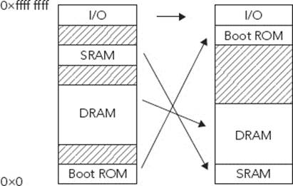
ARM systems also have a distinct use for memory management. ARM CPUs boot from memory location 0x00000000 (or 0xffff0000 if high vectors are enabled), but this presents a problem. 0x00000000 must be located in ROM on first boot, but it is often useful, if not required, to change the vector table later, meaning that it must be located in RAM. In this case, MMUs can be used to remap the memory; to place the boot ROM elsewhere in memory, and to map fast memory to the position of the vector table. This is illustrated in Figure 3-4.
FIGURE 3-4: Memory remapping example
What Is Virtual Memory?
Every address generated by the processor is a virtual address. When the MMU is not enabled, either in reset state or because it was never configured, the memory is flat mapped between virtual and physical. When the MMU is configured and enabled, the processor requests are “translated” by the MMU without the processor actually knowing about the modification. The CPU might think that it is retrieving memory from the DDR2 chip at location 0x2080f080, but the MMU might have changed the request to 0x9080f080.
How Does the MMU Work?
The MMU needs information about the different translations, and to do that, it needs a set of translation tables. This is a zone in memory that contains information about the translations, separated into different sizes.
ARM MMUs support entries in the translation tables that can represent a 1 MB Section, a 64 KB Large page, a 4 KB Small page, or a 1 KB tiny page.
The first part of the table is known as the first-level table. It divides the full 4 GB address space into 4096 1 MB Sections, the largest size available. At the least, an MMU page table should contain these 4096 Section descriptors.
Each entry is called a first-level descriptor and can be one of four different items:
A 1 MB Section translation entry, mapping a 1 MB region to a 1 MB physical region
An entry to a second-level table for more precision
Part of a 16 Mb Supersection
A fault entry that’s a 1 MB Section of unreadable data
Each of the 4096 entries describes memory access for a 1 MB Section. Of course, sometimes it is necessary to have a much smaller zone, for example, to have a 1 KB zone at the end of the stack to cause an exception if the stack grows too much, instead of potentially overwriting code or data. That is why a first-level descriptor can point to another memory location, containing a second-level table.
All this data is stored in system memory, but the MMU contains a small cache, the Translation Lookaside Buffer (TLB). When the MMU receives a memory request, it first looks in the TLB and resorts to reading in descriptors only from the tables in main memory if no match is found in the TLB. Reading from main memory often has an impact on performance, so fast access to some translations can become critical. A real-time system may need to access data in a specific region quickly but not often. In the normal case, when a TLB entry is not used, it is replaced by another line that is used often. To react as quickly as possible, therefore, some TLB entries can be locked, meaning that they will always be present and never replaced.
PRESENTING DIFFERENT TECHNOLOGIES
The term technology refers to technological advances integrated as default over time. For example, when ARM introduced the Thumb technology, it was an option for the ARM7 processor (used in the ARM7TDMI). Thumb is now included by default in the ARMv5T architecture and all later versions.
JTAG Debug (D)
The Joint Test Action Group (JTAG) was an industry group formed in 1985 and whose aim was to develop a method to test circuit boards after manufacture. At that time, multilayer printed circuit boards were becoming the norm, and testing was extremely complicated because most pathways were not available to probes. JTAG promised to be a way to test a circuit board to detect faulty connections.
In 1990, Intel released the 80486, with integrated JTAG support, which led to the industry quickly adopting the technology. Although JTAG was originally designed just to test a card, new uses were studied, especially debugging. JTAG can access memory and is frequently used to flash firmware. Coupled with the EmbeddedICE debugging attribute, it provides a powerful interface.
Enhanced DSP (E)
As ARM-powered devices were used for more and more digital media applications, it was necessary to boost the ARM instruction set by adding DSP instructions, as well as SIMD instructions.
Digital signal processing (DSP) is the mathematical manipulation of information to modify or improve it in some way. The goal of DSP is usually to measure, filter, and/or compress/decompress real-world analog signals. For example, DSP is used for music players, not only converting a compressed digital file into analog music, but beforehand by converting an analog sound, recorded in a studio, into a digital format. Typical applications are audio compression, digital image processing, speech processing, or general digital communications. The use of SIMD instructions can lead to increased performance of up to 75 percent.
DSP can be done on just about any processor, but the routines are extremely repetitive and time-consuming. By adding specialized instructions, more calculations can be done with less processing power. Some of the early mp3 players used ARM7EJ-S, with enhanced DSP instructions. The DSP instructions enabled mp3 decoding at low speeds with little battery usage, ideal for mobile devices. ARM released a highly optimized mp3 software library, but enhanced DSP works for almost all digital information signals. The DIGIC processor is Canon’s processor for its line of digital cameras. The Canon EOS 5D Mark III is a professional 22 megapixel camera, and by using a DIGIC 5, it can take 6 photos a second, apply noise reduction routines, save each image in raw output, and also convert it into JPEG, while keeping enough processor power available to keep the camera’s functions running, notably the auto-focus based on the analysis of 63 points.
On Cortex-A class processors, this has been enhanced with NEON, optionally present on Cortex-A processors.
Vector Floating Point (F)
Vector Floating Point was introduced enabling hardware support for half-, single-, and double-precision floating points. It was called Vector Floating Point because it was developed primarily for vector operations used in motion control systems or automotive control applications.
Originally developed as VFPv1, it was rapidly replaced by VFPv2 for ARMv5TE, ARMv5TEJ, and ARMv6 architectures. VFPv3 is optionally available in ARMv7-A and ARMv7-R architectures, using either the ARM instruction set or Thumb and ThumbEE. A synthesizable version was made available, the VFP9-S, as a soft coprocessor for the ARM9E family.
EmbeddedICE (I)
EmbeddedICE is a powerful debug environment, and cores supporting the EmbeddedICE technology have a macrocell included inside the ARM core for enhanced debugging.
The EmbeddedICE macrocell contains two real-time watchpoint units that can halt the execution of instructions by the core. The watchpoint units can be programmed to break under certain conditions, when values match the address bus, the data bus, or various signals. The watchpoints units can also be programmed to activate on data access (watchpoint) or instruction fetches (breakpoint).
Jazelle (J)
The Jazelle DBX (Direct Bytecode eXecution) was a technique that enabled Java bytecode to be executed directly on an ARM processor. With the advances in processor technology, it was no longer required to have specific Java bytecode acceleration, and this technology is now deprecated.
The first implementation of this technology was in the ARMv5TEJ architecture, with the first processor being the ARM 926EJ-S. At the time, ARM processors dominated the mobile phone sector, as it still does today. Mobile phones were becoming more and more advanced, and users were demanding more and more features. New programs and games could be installed onto a mobile phone, enhancing the user experience. These applications were mainly written in Java ME, a special form of Java designed for embedded systems.
Long Multiply (M)
M variants of ARM cores contain extended multiplication hardware. This provides three enhancements over the previous methods:
An 8-bit Booth’s Algorithm was used, meaning that multiplications were carried out faster, a maximum of 5 cycles.
The early termination method was improved, meaning that some multiplications could finish faster under specific conditions.
64-bit multiplication from two 32-bit operands was made possible by putting the result into a pair of registers.
This technology was made standard for ARM cores using architecture ARMv4 and above, and ARM9 introduced a faster 2-cycle multiplier.
Thumb (T)
Thumb is a second instruction set generated by re-encoding a subset of the ARM instruction set in 16-bit format. Because it is an extension of ARM, it was logical to call it Thumb.
Thumb introduced 16-bit codes, increasing code density. On some systems, the memory was 16-bits wide, so it made sense to use 16-bit instructions. Reducing instructions to 16 bit also meant making sacrifices, so only branch instructions can be conditional, and only registers r0 to r7 are available to most instructions. The first processor to include Thumb was the ARM7TDMI. This chip went on to power devices like the Apple iPod, the Nintendo Game Boy Advance, and most of Nokia’s mobile phone range at the time. All ARM9 processors and above include Thumb by default.
Thumb-2 technology was introduced in the ARM1156T2-S core and extends the limited 16-bit instruction set by adding 32-bit instructions. Thumb with Thumb-2 is a “complete” instruction set in the sense that it is possible to access all machine features, including exception handling, without recourse to the ARM instruction set.
Synthesizable (S)
ARM licenses their IP, and it is normally delivered in a hard-macro format. Some are synthesizable cores and are delivered to clients in source code form. Synthesizable cores can be flashed onto an FPGA component, and users can add their peripherals to the ARM core before flashing and testing. This can be extremely useful for prototyping and to create small series of processors, since some manufacturers provide FPGA chips with an embedded ARM core and enough programmable logic to add a large range of peripherals. Changes can be tested, and when the logic development is complete, the FPGA chips can be flashed with a final configuration — a custom design without buying an ARM license.
Soft-cores enable greater flexibility but often come at the price of speed. Soft-cores are normally clocked at a slower speed than hard-core variants but have significant advantages.
Today, an ASIC may integrate an entire processor, RAM, ROM, and several peripherals all on one chip and are all user definable. ARM synthesizable cores allow companies to make optimized ARM cores based on the design goal of the company. The core can be optimized for power consumption, performance, cache size — almost all processor parameters can be customized. The flexibility provided by this solution can be seen in the huge ARM ecosystem, where a large number of products exist with different characteristics, but all based on the ARM core.
Synthesizable cores started with the ARM7TDMI-S and exist for some ARM9, ARM10, ARM11, and Cortex cores. Today, almost all ARM cores are delivered in synthesizable forms to ARM licensees.
TrustZone
TrustZone is a security technology implemented by ARM on the ARM1176JZ-S and now an integral part of every Cortex-A class processor.
TrustZone is an approach to security by creating a second environment protected from the main operating system. Trusted applications run in a Trusted Execution Environment and are isolated by hardware. Designed for mobile applications, TrustZone enables users to run unsafe code, while protecting the core functionality.
For example, mobile telephone manufacturers often require this sort of functionality. On a mobile phone, it is quite possible to have two operating systems that run simultaneously. One of them is the “main” operating system, the system that is visually present on the screen, and enables you to download and install programs from the Internet. This environment is not secure; it is possible to download malware despite best intentions. A second operating system, this time a real-time OS, is responsible for the hardware side of the telephone, the modem. Both systems are separated for several reasons: partly because of the operating system (for example, Android can’t be compiled for every modem on the market); and secondly for security, the operating system must not have access to core systems. Mobile telephone manufacturers don’t like it when you flash a new version of the operating system or have access to factory settings. This is one of the fields where this technology can be useful.
NEON
NEON is ARM’s wide Single Instruction Multiple Data (SIMD) instruction set. Historically, computers have always been running one single task at a time. An application may require millions of calculations, and each calculation will be done one at a time. In normal circumstances, this works fine. When working on multimedia files, this proved to be slow and in need of some optimization. Now say, for example, you want to turn a graphics image into a black-and-white image. You might look at each pixel, take the red, green, and blue components, take the weighted average, and then write back the data. For a 320×256 pixel image, you would have to do this 81,920 times. That isn’t too bad. When working on a Full HD image, you are working on a 1920×1080 pixel image, meaning 2 million calculations. This is beginning to become huge. A 22-megapixel camera will output files in the range of 5760×3840 — 22 megapixels, so 22 million calculations. Suddenly, this becomes painfully slow. By using NEON instructions, operations can be done on multiple values packed into registers in a single cycle, allowing for higher performance.
big.LITTLE
ARM big.LITTLE processing is ARM’s answer to mobile devices’ energy consumption. Today’s always-on mobile devices are difficult to predict, sometimes requiring little processing power and sometimes requiring enormous amounts of power. Take the example of a tablet with an estimated 8 hours of battery life. On standby, even if the screen is off, the device is still running in the background, connecting to Wi-Fi every so often to fetch e-mails, allowing some programs to run in the background, and especially, running an alarm clock that will go off in 10 minutes to wake you up. And it does. The screen turns on, an alarm sounds, and the device says good morning the best it can. Up until now, you haven’t done anything actually CPU-intensive; a low-powered CPU could do the job just fine. One hour later, you are on a flight on the way to your vacation destination, and to kill time, you start playing a game. Now things start to change. The CPU is being used intensively, and power consumption goes up. The processor adapts by increasing the clock rate, and you get the most out of your tablet. One hour later, you still aren’t past the last level, but they start serving drinks, so you put your tablet down. The operating system detects that you no longer need as much processing power as you did before, and it scales down the frequency, therefore using less power. The problem with this is simple: More powerful processors use more energy, no matter what the clock frequency is. Even when doing “nothing,” there is still more silicon to power, and each clock cycle does more and more things, costing energy. Running your application on a Cortex-A7 will cost less energy than a Cortex A-15, meaning more battery life, but the Cortex-A15 is more powerful than a Cortex-A7, meaning better applications. The ideal solution would be to have a Cortex-A15 that has the battery life of a Cortex-A7, but that isn’t possible. It is, however, possible to have a Cortex-A15 and a Cortex-A7 in the same chip. Enter ARM’s big.LITTLE technology.
ARM’s big.LITTLE works on the principle that both processors are architecturally identical. Because both processors have the same architecture, they can also have the same applications that can, if needed, switch from one processor to another. Processes switch between the two processors, depending on what is needed and depending on instructions issued by the kernel. When using background applications, applications are run on the low-powered CPU, and when the system is under load, the processes are run on the faster CPU. ARM estimates that by using this technology, substantial energy savings can be achieved. In ARM’s tests, web browsing used 50 percent less power, and background tasks, such as mp3 playing, used 70 percent less energy. All this is achieved transparently for applications; software changes are made only in the operating system’s kernel scheduler. Software doesn’t even need to know if it is running on a big.LITTLE enabled processor.
SUMMARY
In this chapter, I have explained the different subsystems of an ARM processor, and provided an explanation of the different options available on select processors. I have presented how the processor starts, what the vector table is, and how it is used for exceptions, I have explained the different registers and which ones are reserved, before presenting some service registers, and finally, basic memory management.
In the next chapter, I will give a brief introduction to assembly language, with an explanation of what it is used for and how it is still essential to know assembly for embedded systems. I will also go through an example assembly program, but please don’t run away! Assembly isn’t that difficult, and it can even be fun.
All materials on the site are licensed Creative Commons Attribution-Sharealike 3.0 Unported CC BY-SA 3.0 & GNU Free Documentation License (GFDL)
If you are the copyright holder of any material contained on our site and intend to remove it, please contact our site administrator for approval.
© 2016-2026 All site design rights belong to S.Y.A.