Make: AVR Programming (2014)
Part III. Advanced AVR Topics
Chapter 16. SPI
Interfacing with External Memory
So far, when we’ve been talking serial, we’ve really meant the kind of old-school asynchronous serial protocol that’s based on RS-232, which is how computers used to talk to printers in the 1970s. But there are other serial data transfer modes out there, more or less appropriate in different situations.
In this chapter and the next, we’ll look at two modern serial protocols. This chapter deals with the serial peripheral interface (SPI), which is blindingly fast and better suited for a small number of devices. The other protocol, I2C (“inter integrated circuit”), has an addressing scheme and is easily extended to a network of up to 128 devices using only two wires (and ground), but is a lot slower than SPI.
From a user’s perspective, however, most of the time you’ve got a cool new device and you just want to talk to it. The peripheral devices that need speed will speak SPI and those that play well with others will speak the I2C protocols, so you’re going to need to learn to use both of them. Fortunately, because these protocols are so widespread, our AVR microcontrollers have internal hardware that makes coding for them a breeze once you know how. That’s what this chapter and the next are all about.
This chapter gets your AVR chip talking SPI serial with an external EEPROM chip. We’re building up toward a standalone data logger application by the end of Chapter 17, and we’re going to need a bunch of nonvolatile memory to store the data in. External EEPROMs and other flash-memory devices provide a cheap and easy way to keep lots of data around even when the power goes out, so they’re worth knowing about in their own right. But if you’re not so interested in the particular application, just think of the EEPROM as a generic SPI device and you’ll still learn something useful.
WHAT YOU NEED
In addition to the basic kit, you will need:
§ An SPI device to talk to. Here, I’m using a 25LC256 32K SPI EEPROM chip because they’re cheap and similar to many other off-board memory devices.
§ A USB-Serial adapter.
How SPI Works
I love the SPI (serial peripheral interface) bus protocol. It’s like a shark, brutally efficient at what it does, and essentially stripped of all frills. When you want to move a lot of data really fast between a few devices, it’s hard to beat SPI.
One reason that SPI is so fast is that, unlike our old friend UART, it’s a clocked, or synchronous, protocol. With UART, we were always worried about a baud rate, the rate at which to transmit and expect data. The transmitting and receiving devices have to be precisely in sync, agreeing on when to set and read the voltage levels on the transmit and receive lines. And this means that UART serial can only transmit data as quickly as the two devices can agree on the timing, which limits the speed to a few hundred thousand bits per second at best. (We’ve been running at 9,600 baud, which is a little conservative; it’s about 1/10th of the fastest UART speed.)
With SPI, in addition to the transmitting and receiving lines, there’s a third wire that’s used as a clock line that synchronizes the two communicating devices. This way, both can agree that they’ll read and write data on the positive voltage transition, for instance. This means that the bit rate can be as fast as the two devices can agree on a rising voltage edge. SPI speeds usually start at 1 megahertz, and 10 megahertz is pretty much standard. That’s a hundred times faster than the fastest asynchronous serial setups, and a thousand times faster than what we’re using for UART. And these days it’s not uncommon to have SPI buses in consumer electronics devices running as fast as 50–100 MHz. That’s really, really fast.
The other reason that SPI can be so fast is that there’s almost no overhead, and thus no extra work for the CPU to do to make use of the data as it comes across. Our old serial protocol relied on a start bit and a stop bit to keep synchronized and to delimit the bytes one from the next. This means that for every 8 bits of data, 10 signals need to be sent, which further slows it down. This data framing--knowing where one byte starts and the previous one ends—is handled by yet another wire in SPI.
So if you’ve been following along so far, you’ve got the picture that SPI is fast, but you’ve probably also counted at least four wires necessary for SPI: a clock line, two data lines (one for each direction), and a fourth line that’s used to signal the start and end of a transaction. That’s the design trade-off with SPI; it’s a simple protocol that’s brutally fast, but requires a lot of wires. It’s time for some diagrams and definitions.
The most common type of SPI bus setup looks something like Figure 16-1. A master device is responsible for generating the clock signal (SCK) that all of the slave devices receive. Both master and slave devices use the clock signal to synchronize their voltage signals on the MOSI, or “master-out-slave-in,” and MISO, or “master-in-slave-out,” data lines. The data direction on the two lines should be obvious, which is another reason to love SPI, but just to be sure, the master sets the voltage on MOSI, and the slave sets the voltage level on MISO. (I also drew little arrows for you.)
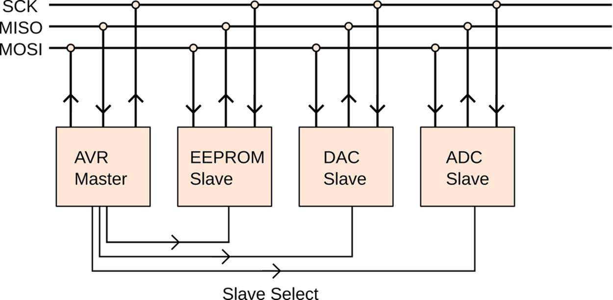
Figure 16-1. The SPI bus
Rounding out the signal lines, the slave-select (or chip-select) lines control which slave device is currently active. Note that there is one slave-select line per slave device. On an SPI bus, all the chips can be connected to the same SCK, MISO, and MOSI wires, but each target chip also has to have its own chip select line. This requirement of one extra wire per device is what keeps SPI basically limited to small networks, or forces you to use trickery like port expanders to address all of the devices.
If you’re writing your own SPI from scratch, and not using the AVR’s dedicated hardware SPI, you should also know that the slave-select lines use inverse logic. That is, the slave-select lines are normally held at the high voltage level and are dropped down to ground to signal who’s turn it is to speak.
Now, the SPI bus protocol is strange in one way, and understanding this strangeness is key to writing code that’ll eventually use SPI, so pay extra close attention right now. Despite the rather dramatic naming choice for the two devices, both “master” and “slave” devices do exactly the same thing—on one edge of the timing clock, they set up one bit for output, and on the next edge of the timing clock, they read one bit in as input. It’s just that the master, as noted previously, is responsible for generating the clock signal and deciding which slave to speak to.
Let me say that again, because it’s the key to understanding SPI. With every clock tick, both the master and the slave transmit and receive a bit of data on their respective lines. Consequently, there’s no real concept of separate “send” and “receive” actions in SPI—both are sending and receiving all the time. I like to think of it as “bit trading.”
Bit Trading Example
As an example, imagine that you’re communicating with a device that that takes in an 8-bit command and returns 16 bits of response data. If the AVR is the master device, it needs to set up its data line and clock out 8 bits of data in a row. At the same time, it’s just received an 8-bit byte from the slave device, but because the slave hadn’t received the command yet, the byte probably isn’t meaningful. The AVR can probably throw it away.
After clocking out the 8-bit command string, the AVR needs to clock out 16 more bits of data to the slave, during which time the slave will send its 16-bit response back to the AVR. For these 16 bits, the slave probably doesn’t care what the AVR is sending, but it needs to receive the clock signal so that it can transmit its bits. This is bit trading; the AVR needs to send out 16 bits to get 16 bits back. It probably doesn’t matter what bits the AVR sends, though it’s customary to send all zeros when you’re just waiting for a response.
I say “probably” because there are some slave devices that are smart enough to receive the next command while still sending the response to the previous one, effectively doubling the data throughput. When this is the case, it can be tricky to keep the timing of command and response straight. This is why it can help to bear in mind the simultaneous bit-for-bit trading nature of SPI.
The other time that the SPI bus can seem strange is when you’re dealing with sensors. Some devices, like temperature sensors, for instance, don’t really take any input and are designed as slave devices. Because of the way SPI works, the AVR master has to senddata—any data—to the sensor in order to get data back. The sensor ignores this data and is just using it for the clock source; but from the perspective of the AVR, it may seem odd to send data to your sensor. Keep in mind the way SPI works under the hood, that you’re really bit trading, and this won’t seem so strange.
Shift Registers
If you’d like to take a deeper look into the SPI bus, you’ll need to understand shift registers, because shift registers are what let the devices on an SPI bus convert data between serial data (one bit at a time) and parallel data (all eight bits at once).
The AVR’s CPU—and whatever the CPU is connected to—wants to work with bytes. Rather than connecting them together with eight wires (which we’d probably call a “parallel data cable”) and simultaneously transmitting a bit on each wire, it’s physically simpler to send the bytes one bit at a time (in serial) over just one or two wires, and then reassemble the received bits into our 8-bit byte after they’ve all arrived. The circuit that does this serial-to-parallel and parallel-to-serial conversion is a shift register, which is basically eight clocked one-bit memories arranged in a row. When the clock ticks, each memory cell takes on logic value that the cell to the left of it had. How does this work?
Imagine eight people standing in a line, and a ninth person who’s handing them red or blue rocks. When a clock ticks, everyone passes their rock to the right down the line. After eight clock ticks, each of the eight people will have rocks whose color depends on the sequence of rocks that were fed in one at a time. Now you can read out the data that came in one bit at a time, but all together as an 8-bit byte—a serial-to-parallel conversion.
In Figure 16-2, the serial sequence “1,0,1,0,0,0,0,0” was clocked in one bit at a time. After eight clock ticks, you can read the parallel value out (in mirror-image).
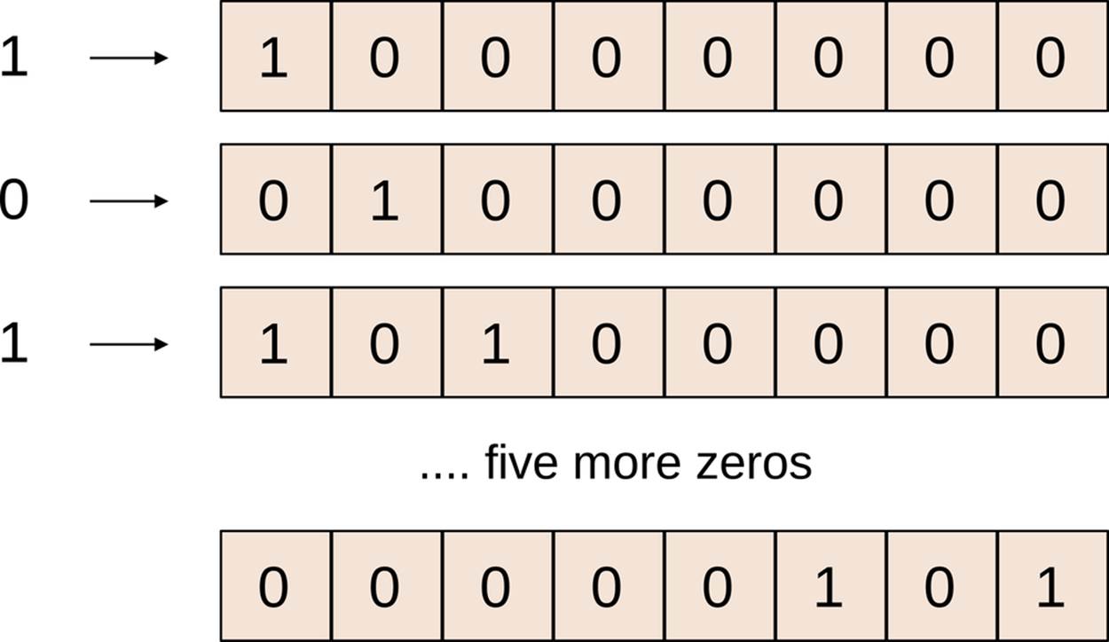
Figure 16-2. A shift register
Some shift registers also operate the other way around: parallel in, and serial out. You can load up all eight memory cells at once and then read out the value of the rightmost memory cell as you advance the clock. The output is then a serialized version of the same pattern of bits that you loaded in. “Universal” shift registers let you both read and write to the register in parallel, making them serial-to-parallel or parallel-to-serial converters.
And this is why I love the SPI protocol: it’s just two of these universal shift registers linked together in a loop. Both the master and slave have a shift register, and the input of each is connected to the output of the other through the MOSI and MISO lines so that they form a ring. See Figure 16-3.
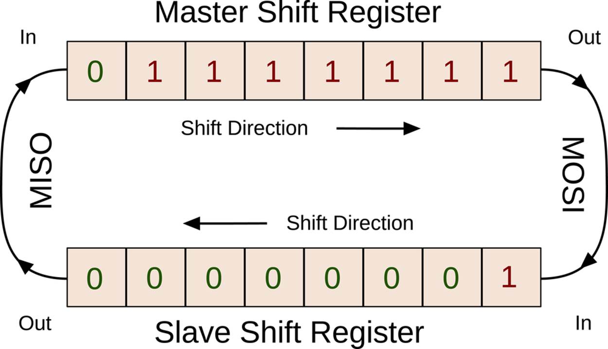
Figure 16-3. SPI is shift registers
Both devices’ shift registers start out parallel-loaded with the data that they’re going to transmit. In this example, the slave is loaded with all zeros, and the master all ones. After one clock tick, the master is left with seven of its original bits and the first one that’s come in from the slave, and vice versa, because it’s completely symmetric.
After a total of eight clock ticks, all eight bits of each byte have traded places. Because the two shift registers are universal, the respective processors can read them out as a single byte, in parallel. Once that byte is processed, the registers are reloaded, and the next bytes are ready to move around the circle.
OTHER USES OF SHIFT REGISTERS
Shift registers are good for more than SPI and serializing data streams. In fact, given that input and output pins on AVR microcontrollers are often scarce in my designs, shift registers are an essential part of my electronics-design toolkit.
First, let’s think about how a shift register could be used as an output-pin multiplier. With two pins, you can shift eight bits of data into a shift register one at a time. If it’s important that none of the outputs change until they have the full data, there are shift registers that have additional enable lines that only latch the data into an output register once all eight (or however many) bits have been clocked in.
So say you need to light up 16 LEDs in particular patterns. One way to do this is with one AVR output pin per LED, but that uses up almost all of the pins on the AVR. Using shift registers, you can be a lot more clever. If you use one 8-bit shift register, you only need two pins, data and clock, to control all eight bits of output from the register. Naively, you could just hook up another two pins to another shift register, and you’ve got all 16 LEDs under control with only four AVR pins.
But you can do better. If you can shift the bits in fast enough that the blinking isn’t noticeable on the output, you can chain the two shift registers together, wiring up the output of the eigth bit of the first register to the input of the second. This way you’re driving all 16 outputs with just the same two pins. And if you need simultaneous change on all 16 outputs, you can use shift registers with an output register, for the cost of only one more AVR pin to toggle their enable pins.
Now if that’s not good enough, remember that the AVR’s hardware SPI peripheral is built to take in eight bits and clock them out to a shift register in the receiving peripheral. Usually, we’re thinking of a memory chip, sensor, DAC, or other “real” peripherals. But we can also use the SPI to talk to plain-old shift registers, for pin-multiplying purposes.
When you want to load up a particular pattern of eight bits on a generic shift register using the SPI hardware, all you have to do is connect the MOSI to the shift register’s input, write the byte to the SPDR data register, and watch it go. And remember, the hardware SPI is very fast—transmitting the bits at megahertz rather than mere kilohertz.
The 74HC595 is a very common 8-bit serial-in, parallel-out shift register with built-in a storage register. They sell for 15–20 US cents each, and half of that in bulk. You can cascade as many of these as you need to multiply your AVR pins’ output capabilities. In many applications, you’ll find that the AVR’s output pins are scarce. When this is the case, combined with the AVR’s dedicated SPI hardware, a shift register can be your very best friend.
And of course, there’s a parallel-to-serial equivalent shift register, the 74HC165 chip, that you can use to effectively multiply the number of digital inputs the AVR can have. As previously, you can use the SPI hardware to read in bytes from the shift registers, taking in parallel data when latched, shifting it into the AVR’s SPI register one bit at a time, and then reading the full byte out in your code. It’s essentially the same trick, just in reverse. If you find yourself needing a parallel-to-serial input expander, the 74HC165 chip is a good bet.
SHIFT REGISTERS DRIVING SHIFT REGISTERS
Here’s where it gets meta! Remember that we had an issue with a proliferation of slave-select lines in a big SPI network? You can solve this by using a shift register connected to the slave-select lines, and addressing the shift register with the AVR SPI hardware. This is not for the faint of heart, but it’s an elegant solution to a common problem.
To select a slave device, you first slave-select the shift register and send it the right byte to drop the desired device’s slave-select line. When you latch in this address byte and deselect the shift register, the SPI bus is set up to talk to your slave device. This trick lets you easily address eight devices on your SPI bus with nothing more than the normal four AVR SPI pins and a shift register.
EEPROM External Memory
Because the SPI bus is fast, you’ll find that it’s mostly used by devices that need speed: ADCs and DACs for audio or much faster signals, output expanders, and memory. In this section, we’ll work on a demonstration of the AVR’s SPI capabilities using an offboard SPI EEPROM memory chip that’ll let us store 32 KB of data. (OK, that’s not a lot, but similar principles take you up into the gigabytes because SD/MMC flash memory cards have an SPI interface.)
External Memory
When you need to store more data than you’ve got space for inside the AVR chip, it’s time to look to external memory. There are two main types of external memory: voltaile types that rely on constant power to remember their data, and nonvolatile memory that is slower and more expensive but retains its data even when the lights go out.
Volatile memory (SRAM, DRAM, etc.)
There are all sorts of electronic tricks for storing bits of information as voltages. Static random access memory (SRAM) and dynamic random access memory (DRAM) take two different approaches to storing your bits. SRAM uses a network of transistors that hold the last voltage level that was imposed on them—as long as the power stays connected.
DRAM, on the other hand, charges or discharges one tiny capacitor per bit to store the logical one or zero. This means that dynamic RAM’s many capacitors need periodic reading and recharging, a cycle called a “memory refresh,” which static RAM doesn’t.
Both rely on power to retain data—cut the power, and poof! The data stored in memory is gone. These two types of memory can be quite cheap per megabyte, and read and write quickly—SRAM has a slight speed advantage.
Dynamic RAM is a lot cheaper for large memories, but the necessary refresh circuitry makes it impractical for small microcontroller designs. For use with a microcontroller, static RAM is the easiest way to go when you need a lot of fast storage but don’t mind losing it when the power is off. In particular, Microchip makes a range of 23Kxxx SPI serial SRAM chips that can be used just like the EEPROM in this chapter, but they run on lower voltage, which complicates the power supply.
EEPROM
EEPROM (electrically erasable programmable read-only memory) is probably the most flexible type of external memory, although it’s not particularly cheap or fast. The advantage that it does have, though, it that EEPROM is nonvolatile (doesn’t go away when the power is turned off) and there are plenty of chips available that run on 5 V supplies without level conversion. EEPROM, like the one we’re using in this chapter, can hold its memory for a very long time with no power—Microchip’s datasheet specifies longer than 200 years!
Flash
Flash memory is a newer type of EEPROM that is significantly cheaper and offers faster write times, but at the expense of only being able to write a page of memory at a time. While with generic EEPROM, you can change one byte without modifying its neighbors, with flash memory, the bytes are arranged in pages of multiple (often 512) bytes that must all be written together. So to change one byte, you read all 512 into your microcontroller’s memory, change one byte, and then send them all back out to flash storage.
Because this procedure is power consuming, time consuming, and no fun, there are also flash memory chips that have a small embedded controller inside that takes care of all this for you. When you need more memory that you’re able to get from a plain-vanilla EEPROM, something like Atmel’s AT45 series of flash memories are fantastic. They have onboard SRAM buffers so that you can access one while the other is writing to flash. You can get them with a 66 MHz SPI bus and 2 MB of memory for under $1.50, though you’ll have to supply them with 3.6 V instead of 5 V.
SD cards
Finally, you should know about SD/MMC cards. Under the hood, they’ve got a small processor and a bunch of flash memory. Most SD cards also allow you to read/write to them with SPI. One catch is that, as with the higher-storage Atmel chips, they also need to be run at a lower voltage, usually between 3.0 and 3.6 volts. The other disadvantage is that, being flash chips inside, you have to read and write in 512-byte pages.
On the plus side, the SPI protocol for running SD cards is well documented, and it’s hard to beat 2 GB of storage for only a few bucks. You’ll find tutorials on the Web for how to use SD cards with an AVR, and even how to incorporate a FAT filesystem so that you can easily transfer files to and from your desktop computer.
The memory chip I’ve chosen is one of a family of very common EEPROM chips, the 25LC256 from Microchip. Why? Because it has a decent amount of nonvolatile memory for making a logger, it works on a wide 3.5–5.5 volt range, it’s available as a DIP part for breadboarding, and it’s basically cheap. It’s also part of a family of SPI EEPROMs with memory ranging from 512 bytes to 128 kB. Small(ish) EEPROMS like this are usually used for storing configuration data, but even with just 32 KB, sampling the temperature once every five minutes, we’ll get over three month’s of runtime. Or if we sample temperature every 10 seconds, it’ll run for three and a half days. Thirty-two thousand samples is more than you’d think.
If you look at the datasheet for the 25LC256 chip, it supports exactly six commands: read, write, write-enable, write-disable, read status, and write status. When you’d like to read from the chip’s memory, you first pass it the read command, then the memory start address, and then just keep clocking in/out bytes until you’ve had enough. To write, you first have to send a write-enable command. Then, send the write command, the start address, and then up to 64 bytes of data. When you’re done writing, the AVR raises the voltage of the slave-select line, and the EEPROM flashes the bytes into memory.
There are a couple of complications, which are common to about every memory type out there, so I’ll go into some detail for you. First, writing the received data into memory takes a bit of time. With the 25LC256, it’s guaranteed that a write won’t take more than 5 ms, but that’s quite a long time in microprocessor-land. This is why the EEPROM chip also has a status register and a bit in that register that tells you that it’s busy writing. After you (or the AVR) write a block of data to memory, it’s customary to check up on the status register until the “write-in-process” bit is clear if you need to use the EEPROM again within a short period of time, as is frequently the case when you’re saving a bunch of data.
The other complication is that the memory inside the EEPROM is internally arranged in “pages” of 64 bytes each. Other memory devices, like flash cards or SD cards, will have a similar layout but with different numbers of bytes per page. Because writing to memory is relatively slow, it makes sense to do as much of it at once as possible, but this means that you have to have some internal temporary storage inside the EEPROM device, and that the places it’s going to store the data are simultaneously accessible. Hence, memory pages.
The gotcha with paged memories is that you have to send less than one page of data, or else it wraps around. For example, say we’re going to save eight bytes of data starting at memory location 60. The first four bytes will fit within the page easily, going into locations 60, 61, 62, and 63. The next four bytes, however, will wrap around and get written into memory locations 0, 1, 2, and 3, rather than 64, 65, 66, and 67, because memory locations 64, 65, 66 and 67 don’t exist on that page. Yoiks!
There are a few ways to work with paged memory. The first, and by far the slowest, is to always write one byte at a time. If you can live with (in our case) 5 ms per byte, this is just fine. If you find that you need speed, the fastest method is to accumulate 64 bytes of data together in an array in the AVR and then send them all directly to the same page in EEPROM, only incurring the 5 ms write delay at the end. You can see that this about 64 times faster. All you have to do is make absolutely sure that you start each block at an even multiple of 64 in the EEPROM’s memory address space.
I once built an accelerometer logger that had to write into a memory that had a 512-byte page structure. But I didn’t want to keep all 512 bytes in the AVR’s RAM at once, because it would use up half of what I had available. As a compromise, I always used multiple-of-512 start addresses and sent the bytes over to the flash memory chip as they came, but kept count of how many I’d sent. Once I’d gotten 512 bytes across, the AVR closed the connection with the memory chip, and the flash memory flashed. While the flash wrote the block of 512 bytes into its memory, the AVR had to buffer up a few more data inputs until the flash signalled that it was ready again.
I mention this more complicated example because it’s a common problem with interfacing between integrated circuits (or any kind of production line, or even cooking with friends). If some processes run at different speeds, you often need to have some ability to buffer up data, test when the downstream chips are ready, and then send it as soon as possible.
SPI Demo Hookup
Figure 16-4 demonstrates how to hook up an SPI EEPROM chip on your breadboard.
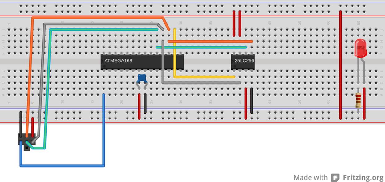
Figure 16-4. SPI EEPROM demo hookup
In order to hook up the 25LC256 EEPROM, you’re going to need to connect power to the chip, naturally. VCC and GND are pins 8 and 4, respectively. There are also two different ways to prevent the chip from working, a write-protect line and a hold line, both of which are active low. So we’ll tie both of these pins (3 and 7) to VCC. Notice that I snuck the VCC rail around to the other side of the chip to make this easier.
Finally, we’ll connect the SPI interface. Pin 1 is the slave select pin (labelled “chip select” in the 25LC256 datasheet), and we’ll connect that to the AVR’s PB2, using the yellow wire in the diagram. SCK is pin 6 on the 25LC256, and goes to AVR PB5, the green wire.MISO (labelled “SO” on the 25LC256 datasheet) is pin 2 and connects to AVR PB4, which is the gray wire. Finally, pin 5 is MOSI (“SI”) and connects to AVR pin PB3 using the orange wire.
You’ve doubtless noticed that we’ve reused the AVR’s programming lines. This is no mistake. The AVR’s self-flashing routines use the SPI bus just as the EEPROM does, only the AVR’s equivalent of a slave-select line is its reset line. And of course, we don’t have to worry about the 25LC256 interfering with the AVR during programming, because its slave-select line will not be pulled low by the AVR.
PULL-UP RESISTORS ON RESET
If you’re having trouble programming the AVR after installing the chip, double-check your connections, and then consider adding a 10k or 100k ohm pull-up resistor between the 25LC256’s pin 1 (slave select) and VCC. This will make sure that the memory chip’s slave select pin doesn’t accidentally get dragged low by the AVR when you’re loading a new program.
Adding a pull-up resistor on a reset or slave-select line is often cheap insurance against startup glitches and other transients. In fact, the Atmel Application Note AVR042 recommends using an external pull-up resistor of greater than 10k ohms on the reset pin in addition to the built-in one. I’ve never had problems related to spurious resets, but if you’re designing a high-reliability application, it’s probably a good idea.
SPI Demo Code
Because I’d like to reuse almost all of the EEPROM memory code in this chapter’s final temperature-logger project, when I worked on the demo project I tried to keep much of the EEPROM-specific code separate from the demo code. What I did was to open up the main spiEEPROMDemo.c file in one window, and the 25LC256.c and 25LC256.h files in another. I had thought about halfway through what functions I’d need—writing, reading bytes to and from the EEPROM, plus whatever was necessary to get that done. By the end, I realized that I wanted a bulk-erase and two-byte read and write facilities. Although I don’t use all of the functions in the demo code, you’ll see how they could be useful later on.
Let’s first take a look at the demo code in Example 16-1. When you’re reading through, notice that almost none of the nitty-gritty of handling the EEPROM memory is present—it’s all handled in the library functions.
Example 16-1. spiEEPROMDemo.c listing
/* SPI EEPROM 25LC256 Demo */
// ------- Preamble -------- //
#include <avr/io.h>
#include <util/delay.h>
#include "pinDefines.h"
#include "macros.h"
#include "USART.h"
#include "25LC256.h"
int main(void) {
uint8_t i;
uint8_t address;
// -------- Inits --------- //
initSPI();
initUSART();
// ------ Event loop ------ //
while (1) {
printString("\r\n==== EEPROM Memory Playground ====\r\n");
printString("Address Value\r\n");
for (i = 0; i < 10; i++) { /* print out first ten bytes of memory */
printString(" ");
printByte(i);
printString(" ");
printByte(EEPROM_readByte(i));
printString("\r\n");
}
printString(" [e] to erase all memory\r\n");
printString(" [w] to write byte to memory\r\n\r\n");
switch (receiveByte()) { /* take input */
case 'e':
printString("Clearing EEPROM, this could take a few seconds.\r\n");
EEPROM_clearAll();
break;
case 'w':
printString("Which memory slot would you like to write to?\r\n");
address = getNumber();
printString("\r\nWhat number would you like to store there?\r\n");
i = getNumber();
EEPROM_writeByte(address, i);
printString("\r\n");
break;
default:
printString("What??\r\n");
}
} /* End event loop */
return (0); /* This line is never reached */
}
First off, you’ll note that we include the 25LC256.h header in the includes section. Just as with the USART.h library that we usually include, we also have to have the 25LC256 code linked in by adding it to the EXTRA_SOURCES list in the makefile.
The first half of the event loop is just printing out over UART. In addition to printing out a menu, a for loop prints out the first 10 memory locations for you to play around with. The remainder of the demo is a switch statement that handles keyboard input, clearing memory, or storing an input into memory. The only EEPROM-specific commands here are EEPROM_readByte and EEPROM_writeByte, and EEPROM_clearAll from the library. And that’s just as it should be: after all, the whole point of writing an EEPROM library is so that I’ll never have to open up the datasheet again!
SPI EEPROM Library Header
So let’s turn to the EEPROM library code. After all, this is where all of the fun SPI stuff happens. Let’s start out with the 25LC256.h file in Example 16-2.
Example 16-2. 25LC256.h Listing
/* SPI EEPROM 25LC256 Library */
#include <avr/io.h>
#include "pinDefines.h"
/* Which pin selects EEPROM as slave? */
#define SLAVE_SELECT SPI_SS_PORT &= ~(1<<SPI_SS);
#define SLAVE_DESELECT SPI_SS_PORT |= (1<<SPI_SS)
// Instruction Set -- from data sheet
#define EEPROM_READ 0b00000011 /* read memory */
#define EEPROM_WRITE 0b00000010 /* write to memory */
#define EEPROM_WRDI 0b00000100 /* write disable */
#define EEPROM_WREN 0b00000110 /* write enable */
#define EEPROM_RDSR 0b00000101 /* read status register */
#define EEPROM_WRSR 0b00000001 /* write status register */
// EEPROM Status Register Bits -- from data sheet
// Use these to parse status register
#define EEPROM_WRITE_IN_PROGRESS 0
#define EEPROM_WRITE_ENABLE_LATCH 1
#define EEPROM_BLOCK_PROTECT_0 2
#define EEPROM_BLOCK_PROTECT_1 3
#define EEPROM_BYTES_PER_PAGE 64
#define EEPROM_BYTES_MAX 0x7FFF
// Functions
void initSPI(void);
/* Init SPI to run EEPROM with phase, polarity = 0,0 */
void SPI_tradeByte(uint8_t byte);
/* Generic. Just loads up HW SPI register and waits */
void EEPROM_send16BitAddress(uint16_t address);
/* splits 16-bit address into 2 bytes, sends both */
uint8_t EEPROM_readStatus(void);
/* reads the EEPROM status register */
void EEPROM_writeEnable(void);
/* helper: sets EEPROM write enable */
uint8_t EEPROM_readByte(uint16_t address);
/* gets a byte from a given memory location */
uint16_t EEPROM_readWord(uint16_t address);
/* gets two bytes from a given memory location */
void EEPROM_writeByte(uint16_t address, uint8_t byte);
/* writes a byte to a given memory location */
void EEPROM_writeWord(uint16_t address, uint16_t word);
/* gets two bytes to a given memory location */
void EEPROM_clearAll(void);
/* sets every byte in memory to zero */
Remember, the idea in C is to store definitions in the header files and keep your code in .c files. In 25LC256.h, I define all of the macros that we’ll be needing to work with the chips.
First, I define SLAVE_SELECT and SLAVE_DESELECT macros. The point here is that if you wanted to hook up your memory chips to use a different chip-select pin in the AVR, you could do so just by changing these two lines, and the rest of the code would work as planned. Next, I make nice mnemonic names for the commands that the SPI memory chip understands. I took these straight out of the memory’s datasheet. I did the same thing with the bit names from the memory’s status register so that I didn’t have to remember which bit is flipped when there’s a write in progress, or the chip is write-protected. Finally, because we’ll be doing page-by-page writes and complete chip erases, I needed to note down the number of bytes per page and the maximum size of the memory.
As you can see, writing a header file like this for new hardware is mainly an exercise in going through the hardware’s datasheet, understanding what it needs, and then making a bunch of definitions that’ll make your life easier when doing the actual programming. And after you’ve done that, you can start to think about what kinds of functions you need to talk to the thing.
Finally, the include file gets to the function prototypes—essentially predefining what all the functions do, what arguments they take, and what type of data they return. Having all the function prototypes in the header file like this is a little bit redundant, but writing them all out is a good exercise for thinking your problem completely through, and having them all written down (and well-commented) is a good resource for later. In principle, you only have to read through the .h file to know how to use the library. (In practice, you’ll almost always have to or want to dive into the code.)
SPI EEPROM Library C Code
Finally, we get to the meat of the code—the C source code that actually talks SPI to the EEPROM. Without further ado, let’s learn some SPI! Follow along with Example 16-3.
Example 16-3. 25LC256.c listing
#include "25LC256.h"
void initSPI(void) {
SPI_SS_DDR |= (1 << SPI_SS); /* set SS output */
SPI_SS_PORT |= (1 << SPI_SS); /* start off not selected (high) */
SPI_MOSI_DDR |= (1 << SPI_MOSI); /* output on MOSI */
SPI_MISO_PORT |= (1 << SPI_MISO); /* pullup on MISO */
SPI_SCK_DDR |= (1 << SPI_SCK); /* output on SCK */
/* Don't have to set phase, polarity b/c
* default works with 25LCxxx chips */
SPCR |= (1 << SPR1); /* div 16, safer for breadboards */
SPCR |= (1 << MSTR); /* clockmaster */
SPCR |= (1 << SPE); /* enable */
}
void SPI_tradeByte(uint8_t byte) {
SPDR = byte; /* SPI starts sending immediately */
loop_until_bit_is_set(SPSR, SPIF); /* wait until done */
/* SPDR now contains the received byte */
}
void EEPROM_send16BitAddress(uint16_t address) {
SPI_tradeByte((uint8_t) (address >> 8)); /* most significant byte */
SPI_tradeByte((uint8_t) address); /* least significant byte */
}
uint8_t EEPROM_readStatus(void) {
SLAVE_SELECT;
SPI_tradeByte(EEPROM_RDSR);
SPI_tradeByte(0); /* clock out eight bits */
SLAVE_DESELECT;
return (SPDR); /* return the result */
}
void EEPROM_writeEnable(void) {
SLAVE_SELECT;
SPI_tradeByte(EEPROM_WREN);
SLAVE_DESELECT;
}
uint8_t EEPROM_readByte(uint16_t address) {
SLAVE_SELECT;
SPI_tradeByte(EEPROM_READ);
EEPROM_send16BitAddress(address);
SPI_tradeByte(0);
SLAVE_DESELECT;
return (SPDR);
}
uint16_t EEPROM_readWord(uint16_t address) {
uint16_t eepromWord;
SLAVE_SELECT;
SPI_tradeByte(EEPROM_READ);
EEPROM_send16BitAddress(address);
SPI_tradeByte(0);
eepromWord = SPDR;
eepromWord = (eepromWord << 8); /* most-sig bit */
SPI_tradeByte(0);
eepromWord += SPDR; /* least-sig bit */
SLAVE_DESELECT;
return (eepromWord);
}
void EEPROM_writeByte(uint16_t address, uint8_t byte) {
EEPROM_writeEnable();
SLAVE_SELECT;
SPI_tradeByte(EEPROM_WRITE);
EEPROM_send16BitAddress(address);
SPI_tradeByte(byte);
SLAVE_DESELECT;
while (EEPROM_readStatus() & _BV(EEPROM_WRITE_IN_PROGRESS)) {;
}
}
void EEPROM_writeWord(uint16_t address, uint16_t word) {
EEPROM_writeEnable();
SLAVE_SELECT;
SPI_tradeByte(EEPROM_WRITE);
EEPROM_send16BitAddress(address);
SPI_tradeByte((uint8_t) (word >> 8));
SPI_tradeByte((uint8_t) word);
SLAVE_DESELECT;
while (EEPROM_readStatus() & _BV(EEPROM_WRITE_IN_PROGRESS)) {;
}
}
void EEPROM_clearAll(void) {
uint8_t i;
uint16_t pageAddress = 0;
while (pageAddress < EEPROM_BYTES_MAX) {
EEPROM_writeEnable();
SLAVE_SELECT;
SPI_tradeByte(EEPROM_WRITE);
EEPROM_send16BitAddress(pageAddress);
for (i = 0; i < EEPROM_BYTES_PER_PAGE; i++) {
SPI_tradeByte(0);
}
SLAVE_DESELECT;
pageAddress += EEPROM_BYTES_PER_PAGE;
while (EEPROM_readStatus() & _BV(EEPROM_WRITE_IN_PROGRESS)) {;
}
}
}
initSPI
The first function is initSPI, which initializes the SPI mode. In this case, it’s terribly simple. We configure all of the pins we’re using for input and output, and then set the clock, master or slave mode, and SPI enable bits in the SPI Control Register, SPCR.
SPI AND OUTPUT PINS
Notice in this code that we first set up the data-direction registers for the pins that we’re using for SPI, and then enable the SPI-specific hardware. This ordering turns out to be crucial, and the source of a very subtle bug that’s caught me twice now.
When the SPI is in master mode, it’s got a provision for deferring to other SPI masters in a multimaster setup. If the AVR has its slave-select pin configured as input (which is the boot-up default) and the pin is toggled low, it goes into a passive SPI mode in order to not interfere with the other masters on the bus. So as long as the slave-select pin is low in master mode, it won’t send out a clock signal.
Because of this, you should enable the pullup on the slave-select pin, even if you’re not using the pin as an output, before you enable SPI mode. Otherwise, you risk random electrical fluctuations shutting down your SPI. In our case, I’m using the SS pin as an output, so I set it as output and set it high before enabling SPI.
One possible complication with other devices is that you’ll have to set up the phase and polarity of the SPI bus lines. In our case, the EEPROM is already configured for operation in the so-called Mode 0, which is the boot-up default for the AVR. Otherwise, you’d have to set up the polarity using the CPOL and CPHA bits. If you find yourself needing to change the SPI data mode, there’s a handy table in the AVR datasheet, Table 18-2, SPI Modes that summarizes it all, along with nice timing diagrams in Tables 18-3 and 18-4. Or read Phases and Polarities.
Setting the clock division bits (SPR1 in our example) is largely unnecessary. After all, we’re running the AVR at 8 MHz, and most SPI devices handle 10 MHz or higher data rates. On the other hand, at higher and higher frequencies, wires become effectively antennas and circuits that should work if designed with short connections on a printed circuit board can fail entirely when you’re using long wires and assembling stuff on a breadboard. So in this example, I’m running the SPI bus at a 1/16th multiplier, or 500 kHz. That’s still plenty fast for transferring memory in and out of our EEPROM, but you should know that we could be running even faster if we needed to.
Did I mention that I love SPI?
PHASES AND POLARITIES
If there’s one complication to the SPI protocol that’s kind of miserable, that’s the question of clock phase and polarity.
The polarity in question just refers to whether the clock signal is normally high and transitions to a low voltage represent the start of a clock tick, or whether the clock signal is normally low, and it’s an rising voltage that signals the start. This isn’t so hard to figure out, and it’s usually just a matter of looking at the device’s datasheet.
Phase is it a little more confusing. Regardless of polarity, clock pulse has two transitions: a leading edge and a trailing edge. The issue of phase is whether to set up the data on the leading edge (and sample on the trailing edge) or to set up the data on the slave-select transition (and be ready to sample by the first leading edge). Phase zero means that the devices sample on the leading clock edge, and phase one means that devices set up on the leading edge.
Combining phase and polarity means that there are four possible SPI “data modes,” and unfortunately you’ll probably see all of them eventually. So here’s my cheat sheet for setting the AVR’s phase and polarity bits, CPHA and CPOL:
1. Figure out the polarity. This is easy to read from the timing diagrams in your device’s datasheet. If the clock idles low, CPOL=0, and if it idles high, CPOL=1.
2. Now look to see when the data is sampled. If it’s sampled on a rising edge, the phase equals the polarity, and you’re in (CPOL, CPHA) = (0,0) or (1,1). If the data is instead set up on a rising edge and sampled on a falling edge, you’re in one of the mixed modes: (CPOL, CPHA) = (0,1) or (1,0).
3. Combine the info from steps 1 and 2, and you should know where you stand.
Alternatively, you may find that the datasheet for your device lists its SPI “data mode.” Mode 0 is (CPOL, CPHA) = (0,0), mode 1 is (0,1), mode 2 is (1,0), and mode 3 is (1,1). The EEPROM we’re using in this example can talk mode 0 or mode 3, and mode 0 is the AVR default, so no configuration is necessary. Score!
Anyway, if you’re at all unsure about the data mode of your SPI devices, try communicating with it. Many devices will send back a status register or device ID string or something that you can use to double-check that you’ve got it right.
SPI_tradeByte
The SPI_tradeByte function takes care of communicating over SPI at the lowest level. Remember that SPI works by clocking two shift registers that are linked together in a loop? Once the SPI is enabled and set to master mode, all that’s necessary to get our byte transferred out, and a new one read in, is to load it into the SPI Data Register SPDR. Now, the AVR’s SPI hardware takes over.
If we want to read the output from the slave device that was sent to us, our code needs to wait for the transaction to finish and then read the SPDR data register, where the outgoing data used to be and the incoming data now resides. All the SPI_tradeByte code does is wait for the transmission to be complete. Reading out the new byte (if you want to) is left for the calling code.
Convenience Functions
The rest of the 25LC256.c file defines a bunch of convenience functions. All of these basically just code up what the EEPROM’s datasheet said to do to talk to it, so I won’t go into all of them in too much detail. However, the basic flavor of an SPI transaction runs through all of them, so it’s worth taking a quick peek.
Look at the function EEPROM_readByte, for example. As with all SPI devices, the EEPROM needs to know when it’s being spoken to, and this is done by sending a digital low voltage over it’s slave-select (or chip-select, depending on the datasheet) line. Then the AVR sends the command to read out memory from the EEPROM, which is defined in the .h file. (Remember, at the same time, the EEPROM is loading up the SPDR with a byte, but we don’t really care what it is.) Next the AVR sends the 16-bit address of where to start reading memory from. Because we do this so often, I wrote a convenience function that breaks up a 16-bit number into two 8-bit bytes and sends them separately.
Having sent the read command and the address, all that remains is to read out some bytes. In this case, the function reads just one and then returns. Note again that the AVR is sending a byte worth of zeros—it had to have something to trade for the EEPROM’s byte. If we wanted to read more bytes, the AVR could keep trading bytes with the EEPROM, and because the EEPROM is in read mode, it would send the next byte out of its memory. In this case, though, we’re happy with one byte, so the function deselects the slave-select line (raising it to a logic high voltage level), and returns the value of SPDR, which has the last value read out from the memory.
The EEPROM_writeByte command is only a bit more complicated. In order to prevent EEPROM memory corruption, you have to first send a write-enable command before issuing the write command. This is done in the usual way—drop the slave-select line, load a byte across to the EEPROM with the write-enable command, and then reraise slave select. Now the EEPROM is ready for writing, and the procedure is similar to reading.
Finally, because writing to an EEPROM can take a few milliseconds, the last line in the write command continually reads the EEPROM’s status byte: dropping the slave line, sending the “read status” command, sending a byte to receive the response, and then reraising slave line at the end. Each time through this cycle, the code checks to see if the write-in-progress bit is set and keeps looping until it isn’t.
Because the EEPROM is structured in 8-bit bytes, like the AVR, it takes a little bit more work to read and write 16-bit numbers, so I wrote convenience functions for these. If you look at EEPROM_readWord for instance, you’ll notice that it’s just about the same asEEPROM_readByte except that there are two calls to SPI_tradeByte(0) after the address is sent, and the return value is a 16-bit data word that’s been reconstituted from the two bytes that get read in.
Finally, there’s a function that erases the entire EEPROM. The fastest way to do this is to start on a page boundary (multiple of 64 in the address space) and load up 64 bytes of zeros, and then write it permanently to memory. Repeating this for every page of 64 bytes in the EEPROM blanks the whole device in minimum time. This function is a good example of the page-by-page style of writing that get the fastest speed out of EEPROMs.
Summary
Using the AVR’s built-in SPI hardware is easy and is definitely the fastest way to get data in and out of the microcontroller. In terms of configuration, it’s not hard at all; in terms of use it is even easier—just write your byte to a register. Here’s a summary:
1. Set up the SCK and MOSI pins (PB5 and PB3, respectively) for output.
2. Set up the MISO pin (PB4) for input, with pullup enabled.
3. If the AVR is the clock master, set the pullup on SS (PB2) if you’re not using the pin as output.
4. Make sure the SPI clock speed is low enough to work with your intended device, and set a speed divider if it’s not, or even if you just don’t need the extra speed.
5. Set the AVR into clock master mode and enable SPI.
6. When you start communicating with a given slave device, begin by flipping its slave-select line low.
7. Now when you want to send a byte to that slave, write it to SPDR, wait for the transaction to end, and read the response back again from SPDR.
8. Finish up a transaction by setting the slave’s slave-select line high again. When you want to talk to another device on the SPI line, simply drop its slave-select line low to start, and away you go.
9. The rest of the details are application-specific. Most devices have their own command sets, address spaces, etc. All of them will be based around sending a series of 8-bit bytes, and all of these should be laid out in their datasheets.
Still, communication between devices can be tricky. When you’re looking at a new peripheral chip, be prepared to sit down with the datasheet for an hour or so. The first step is to turn all of the useful chip-specific commands into nice, readable definitions, and store them in a header file. Then write down all of the transaction types you’ll need, look them up in the datasheet, and start coding and testing.
All materials on the site are licensed Creative Commons Attribution-Sharealike 3.0 Unported CC BY-SA 3.0 & GNU Free Documentation License (GFDL)
If you are the copyright holder of any material contained on our site and intend to remove it, please contact our site administrator for approval.
© 2016-2026 All site design rights belong to S.Y.A.