Practical Electronics: Components and Techniques (2015)
Chapter 9. Active Components
This chapter covers some of the vari- ous types of active components you might encounter, from diodes to ICs—in other words, devices that utilize semiconductors, referred to as solid-state components. We will also discuss some of the package types available for both through-hole and surface-mount components, as well as how to prevent damage to solid-state components from static discharge.
The primary emphasis here is on available types of solid-state devices and the packaging used in their manufacture, not on how these devices work. That would be another complete book (or two) in itself. If you want to know more about the internal operation of active components, take a look at Appendix A or one of the excellent texts listed in Appendix C.
Another key point of this chapter is datasheets. These are the defining documents for electronic components (and many other things as well). Learning to obtain and read a datasheet is a crucial skill for anyone dealing with electronic circuits. To that end, “How to Read a Datasheet” steps through the contents of a typical datasheet and also offers suggestions on where and how to obtain them.
The distinction between an active component and a passive one is based primarily on how a part deals with electrical energy. In Chapter 8, it was described as the difference between something that dissipates energy, or stores and releases energy, without the need for an external source of power, as opposed to something that could actively alter circuit behavior and use an external source of power.
Active components typically rely on an external power source and are able to alter current flow in both linear and nonlinear ways. A transistor, for example, can perform amplification by altering the current flowing through it in proportion to changes in a small input signal. The result is an output that is a larger version of the input. Its behavior is also nonlinear, in that a transistor’s response to an input is based on thresholds and current flow direction. A resistor, on the other hand, will simply resist current flow, no matter how much, from zero up to its physical power dissipation limit. The response graph for a resistor is a straight line, meaning that it is linear. But for a transistor, the voltage-versus-current response curve has distinct curves, and is therefore nonlinear.
Diodes are also included in this chapter, simply because a diode is a semiconductor device with a single solid-state junction and nonlinear behavior. A transistor is a close cousin of the diode with a more complex solid-state junction arrangement. Some texts categorize diodes as passive devices, but because they do exhibit nonlinear responses to current and voltage, I think they can be placed here with the other active components.
How to Read a Datasheet
Before we delve into active solid-state components, it would be a good idea to take a look at the definitive source of information for these parts: the datasheet. Datasheets have become commonplace for things other than transistors, diodes, and ICs; even nuts and bolts have datasheets available. Reading them and making sense of what they contain is what this section is all about.
Datasheets have been around for quite a while. Sometimes called a data sheet or a spec (specifications) sheet, they began as short documents (one page or so) that listed the most important characteristics of a device, product, or mechanism. Over time, they have evolved into elaborate documents that describe the essential electrical, physical, and mechanical characteristics an engineer might need to know in order to use the product. While some datasheets are still only one page (there’s only so much that can be said about a blind rivet, for instance), in other cases, they consist of tens of pages of detailed graphs, tables, and sometimes equations and example program code.
Once, before the Internet made it easy to move electronic documents around, electronic components manufacturers used to spend millions of dollars a year on creating, publishing, and distributing so-called data books, which were generally collections of datasheets for individual components. It was a big day in the lab when a sales representative from a distributor (or even a manufacturer) would show up with a pile of data books in the trunk of her car. It was common to find a wall of bookshelves filled with data books in a well-stocked electronics R&D lab. These days, almost all of those books can fit on a single 16 GB flash drive.
Datasheet authors assume that the reader is conversant with the concepts and terminology used in the datasheet. There is seldom any attempt made to define unique terms or explain concepts. One way to approach this is to get a collection of datasheets from different sources and compare them while having a glossary (such as the one in this book) handy. I haven’t duplicated any datasheets in this section, due primarily to space and copyright considerations, but these documents are readily available from distributor and manufacturer web pages.
Datasheet Organization
Most datasheets for electronic components are organized into multiple sections. I’ve listed six possible sections here, but some may have fewer, and some may have more. It depends to a large extent on the complexity of the part and the internal datasheet style guidelines of each manufacturer:
Summary/Overview
May provide a paragraph or two of overview discussion, a list of features, suggested applications, short summaries of the process technology (how it is fabricated), and other salient points the engineer might want to know at a glance. May also include ordering information if the part is available in different package and temperature range variations, although this information sometimes has its own section.
General Specifications
Typically contains a table of absolute maximum ratings, such as maximum power supply voltage and maximum operating temperature, a table of thermal characteristics, and optimal operating conditions.
Electrical Specifications
May include connection diagrams and a description of the connection pins or input/output terminals, if applicable, and a table of electrical characteristics (min/max operating voltage, clock speed, rise/fall time, and similar data).
Functional Description or Diagram
Some datasheets include a description of the operation of the device from a functional perspective (what it does, not specifically how it does it), or there might be just a functional diagram to illustrate the primary internal functions of the device. If a diagram is included in this part of the datasheet, it can usually be considered to be more of an equivalent circuit diagram (see Appendix A for more on equivalent circuits) than an actual schematic.
Application Examples
In some cases, the designer needs to know some critical details about things like physical mounting, the use of a heatsink, and PCB trace layout considerations. This section might also include what is called a reference design, which is a circuit using the part that is known to work and which can be used as a jumping-off point for the engineer’s own design.
Physical Specifications
This section provides details on available packaging (through-hole, surface-mount, etc.), including dimensions. This is where you look for details concerning correct PCB layout for the type of part you want to use.
Not every datasheet contains all of the sections listed here, or provides them in the order given, but even something as seemingly straightforward as a metal film resistor might have an 11-page datasheet. For example, see the Vishay metal film resistor datasheet. We will look at the datasheet for an IC in detail in the next section, but it is informative to see how datasheets for other types of components are written and organized.
Datasheet Walk-Through
The 555 is a popular (and old!) part first released in 1971 by Signetics as the NE555. It is a timer that uses an RC (resistor-capacitor) time constant (see Appendix A) to control a relatively simple but robust circuit. The 555 can be configured as an astable (continuous) oscillator, or it can be used as a monostable (one-shot) timer. It is an extremely versatile device, and entire books have been written about it (the 555 Timer Applications Source Book by Howard Berlin, for example). For the truly ambitious, there is even a kit that allows you to build a working 555 circuit from discrete components. It’s available from Evil Mad Scientist Laboratories.
As an example, I’ll use the datasheet for a 555 timer IC from Intersil, known as the ICM7555 (or ICM7556 for the dual-timer version). If you want to follow along, you can download the datasheet from Intersil’s website.
The front page contains the general description, a list of features, a list of possible applications, and the package pinout diagrams for both the single-timer and dual-timer versions of the part (the dual timer simply has two complete 555 timers in one package). Figure 9-1 shows a layout diagram of the front page.
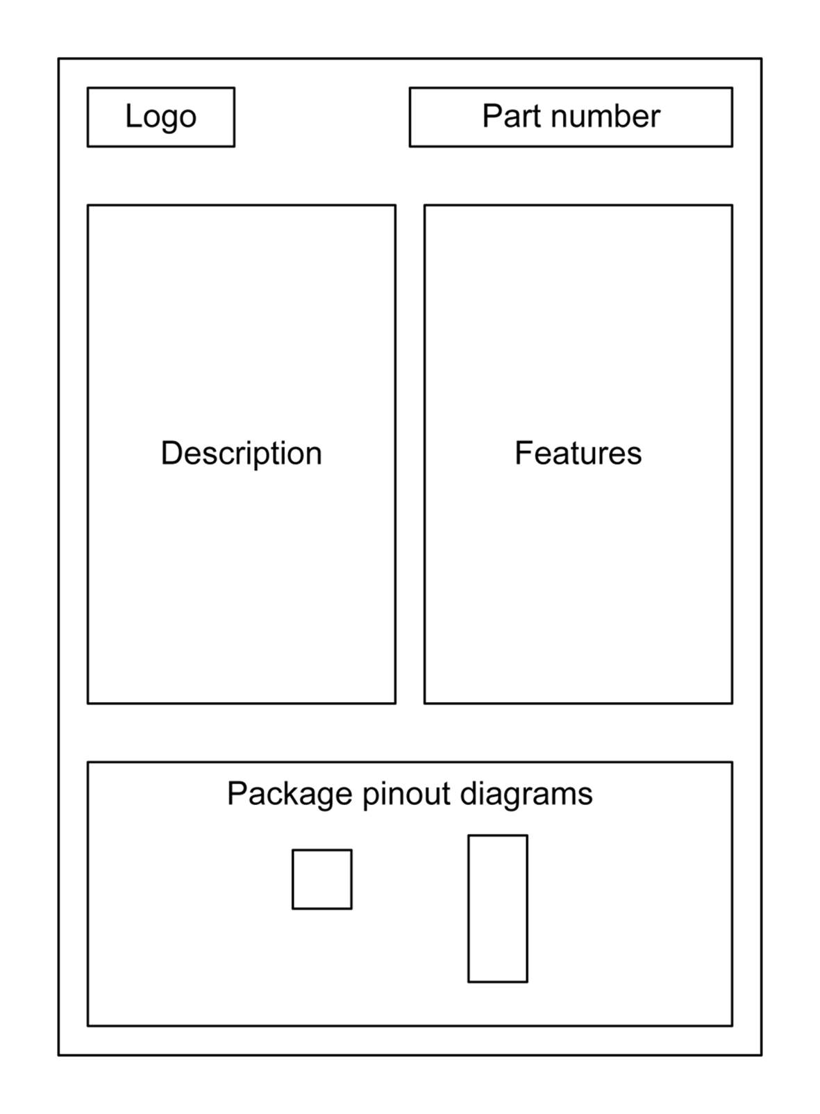
Figure 9-1. Datasheet front-page layout example
This is probably the most important page in the entire datasheet, since it is the one you would want to refer to for pinout information and general specifications, which are incorporated into the list of features in this particular datasheet. After reading this page, we know that the part can operate on a supply voltage from 2V to 18V, it can generate a pulse rate of up to 1 MHz, and it draws around 60 μA of current.
The second page contains ordering information. From this, we can see that the part is available in various package types and three different temperature ranges: 0° to +70°C, –25° to +85°C, and –55° to +125°C. The acronym SOIC stands for small outline IC (a surface-mount package), and PDIP refers to a plastic DIP (dual inline package) through-hole package. The Cerdip package is a ceramic package intended mainly for military and harsh environment applications. “Surface-Mount IC Package Types” describes the SOIC family of packages.
The third page provides absolute maximum ratings and electrical specifications. You might notice that the maximum output current is 100 mA, which implies that the chip will drive an LED or relay without breaking a sweat. The fourth page continues the electrical specifications table and has a functional diagram, along with a truth table that defines the logical behavior for the timer.
But wait a minute, did you catch it? The features list states that the operating current was 60 μA, but the absolute maximum ratings state that the timer could supply 100 mA of output current. There is a big difference between 60 μA and 100 mA. What’s going on here? The answer is shown on page 5 of the datasheet.
Page 5 includes the schematic diagram of the 555 timer. Notice that the output is driven by two MOSFET (metal-oxide semiconductor field effect transistor) devices, one connected to VDD (V+) and the other connected to ground. In other words, the 555 can swing its output from ground to almost full V+ (sometimes also referred to as rail-to-rail). The 100 mA limitation arises from the current-carrying ability of the internal output circuitry on the silicon chip itself. The rest of the timer (everything to the left of the two output MOSFETs) requires only 60 uA to operate.
The applications section, titled “Application Information,” also begins on page 5. This is where you can find practical information about the use of the part. In this case, the datasheet shows three example circuits. Two of the circuits are for an astable oscillator, and the third shows how to use the 555 as a monostable timer. Let’s say you wanted to operate an alarm for some specific period of time and have it turn itself off. You could use a 555 and a relay to accomplish this (see Chapter 10 for information on relays). The circuit shown in figure 3 on page 6 of the datasheet shows how to make a timer, and the text on the page describes how to calculate the values of the RC time constant components. Of course, you could just buy a prebuilt module (such as the one shown in Figure 9-2) that does this, using basically the same concept.
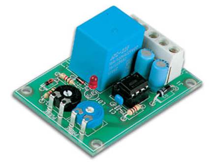
Figure 9-2. 555 timer module kit
The kit shown in Figure 9-2 is available from Apogee Kits for about $5. Other kit suppliers sell similar items for about the same price, so there are many to choose from.
But back to the datasheet. Pages 7 and 8 contain graphs that show the performance of the part for things like minimum trigger pulse width, supply current versus supply voltage, frequency stability versus temperature, and so on. These are good to have, and they provide a way to illustrate the dynamic behaviors of the part as a function of change in various parameters and conditions. In particular, notice in Figures 14 and 15 that if you want to have a wide range of astable frequencies or monostable times, then you’ll need to be able to change the values of the timing components (RA, RB, R, and C) to cover a particular range. A rotary switch can be used to achieve this (see Chapter 6). It’s generally a good idea to at least look through the various graphs provided and see if any of them can tell you something about the part that the equations in an earlier section might not make immediately obvious.
Pages 9, 10, 11, and 12 show detailed package drawings and provide dimensions for each type. Notice that the package descriptions for the 8-pin and 14-pin PDIP parts use the same drawings, so don’t let that fool you. Also, if you’re going to do a PCB layout, this is where you would look to make sure the PCB layout software’s component library has a predefined template that will work with this particular part (see Chapter 15 for a discussion of PCBs). While this isn’t really a big issue with JEDEC (Joint Electron Device Engineering Council) standard through-hole parts, some library templates occasionally get it wrong when it comes to surface-mount components. It’s always a good idea to do a quick check before committing the PCB design to fabrication.
Collecting Datasheets
Once you become familiar with datasheet formats and conventions, they aren’t all that hard to decipher. Just remember that the most commonly referenced information is almost always located at the front, where the designer can get a quick sense of what the part does and what its essential limitations might be. The rest of the datasheet goes into deeper levels of detail, and each datasheet usually wraps up with a description of how the part is packaged.
Of course, none of this is cast in stone, and some datasheets are easier to read than others. Badly written ones are relatively rare, and lack of sales (and customer complaints) will usually get them fixed within a short period of time. Datasheets from major manufacturers are an essential sales tool. They are the first place to look to get information about a part, and almost every manufacturer makes them readily available. Most major distributors also provide links on their web pages to the original datasheets for the parts they sell, and there are websites that offer datasheets for many different parts from multiple sources for free.
After a while, you may find that you have collected a large number of datasheet PDF files. Personally, I like to print out the ones I refer to on a regular basis (double-sided, of course) and put them into a binder (or two, or three). That way, I can make margin notes on the printed pages, and use a highlighter on important sections in the document. But in any case, if you work with electronics long enough, you’ll find that datasheets tend to accumulate. The days of bookshelves full of databooks and three-ring binders may be fading into the past, but the datasheet will be with us for a long time to come in electronic form.
Lastly, lest anyone think that the electronics industry lacks a sense of humor, in 1972, a frustrated engineer at Signetics created a datasheet for a fictional component called a write-only memory device. Signetics was the first company specifically established in 1961 to produce integrated circuits, and it was fairly prolific, so a lot of datasheets for various products were generated each year (the company was purchased by Philips, now known as NXP, in 1975).
The joke datasheet made it through the entire approval process, which verified what the engineer was annoyed about: no one was actually fact-checking the datasheets the engineers submitted. It wasn’t until customers started to call and inquire about availability and pricing that the management at Signetics realized what had happened. They supposedly fixed their internal review process, but I don’t know what became of the frustrated engineer.
Electrostatic Discharge
Electrostatic discharge (ESD) is the bane of solid-state active components. Some devices, such as diodes and rectifiers, are less sensitive than parts like CMOS ICs and FETs (field-effect transistors). But, nonetheless, ESD is something that can wreck a solid-state part if it is handled and stored carelessly. Even worse, a part can sustain ESD damage and still appear to function normally, at least initially. The damage sometimes doesn’t appear until the part is stressed in operation, or after some period of time has elapsed. When it does fail, it will do so without warning.
ESD is, as its name implies, an event that occurs when an accumulated static charge is suddenly discharged to ground (lightning is a form of ESD, albeit a rather dramatic one). The problem arises when the path to ground happens to be through an IC or other solid-state device, and most of the time it can’t even be felt or seen. The first line of defense is to make sure that you are not the source of the static discharge, or part of the discharge path. The easiest way to avoid becoming an ESD source is to wear a wrist strap, like the one shown in Figure 9-3.
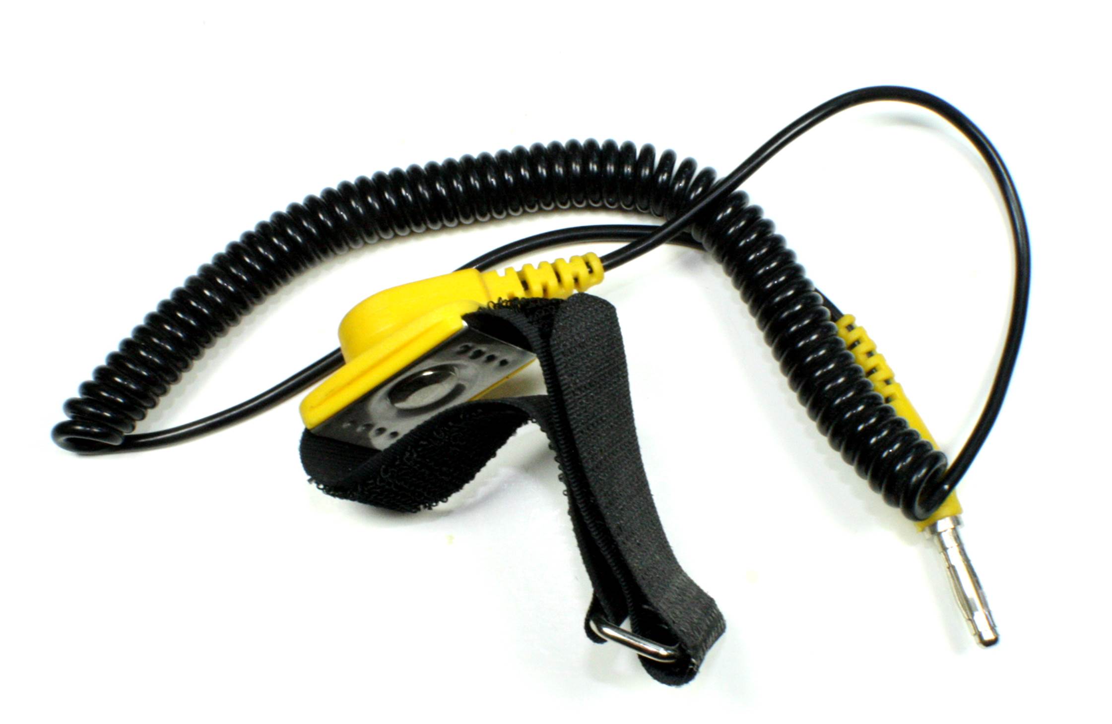
Figure 9-3. A grounded wrist strap to prevent ESD damage
Wrist straps don’t connect directly to ground, but rather through a 1M ohm resistor to limit the current and prevent shock hazards. The resistor also serves to limit the effect of sudden discharge through a part should it be at a high potential when touched by someone wearing the ESD wrist strap. The discharge can work either way, from handler to part, or part to handler.
Another technique is to use an ESD mat. These mats come in a range of sizes and are made of a conductive material. They are designed to cover the surface of a workbench and they can be trimmed to fit a particular space. They have a small terminal in one corner that is connected to a ground point. They typically come in rolls and in a variety of colors.
Soldering equipment is also available in ESD-safe designs, and most better-quality soldering irons and soldering stations have this feature. Ungrounded soldering tools can accumulate a formidable amount of charge, and it can be released into a part as soon as the tip of the iron touches the PCB. For this reason, you should always use an ESD-safe soldering iron or soldering station when working with solid-state components, and never defeat the ground on the AC mains plug.
Lastly, there is the issue of component storage. Storage bins should be ESD safe, if possible. If that’s not practical (or affordable), it is a good idea to have a supply of antistatic high-density foam on hand. Figure 9-4 shows some ICs and a few FETs inserted into a piece of anti-static foam.
The foam is made from a conductive material, usually impregnated with carbon, that acts as a high-value resistor. If you handle the foam with an ESD wrist strap on, and work with it on an antistatic mat, you should be fine. Just remember while wearing the wrist strap to touch the foam first, not the components themselves. This allows the strap to do its job and bleed away any high potential without damaging the parts. You can purchase this type of foam in sheets from most major electronics distributors and ESD-control product suppliers.
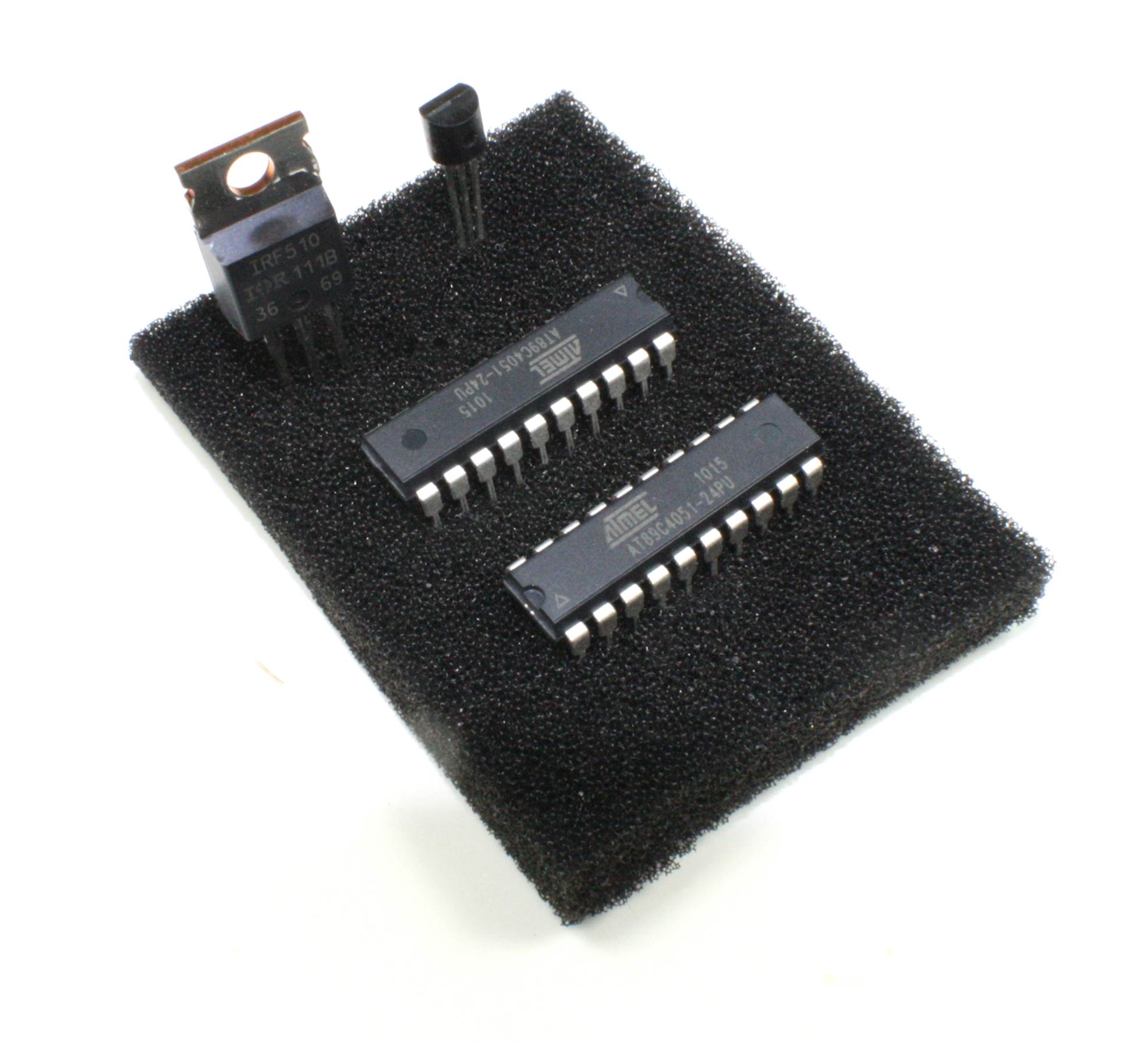
Figure 9-4. Anti-static foam carrying sensitive components
Packaging Overview
Active components come with anywhere from 2 to 144 leads (or more), depending on the device. Small through-hole components such as diodes and rectifiers are often packaged in axial lead forms, much like resistors. Transistors come in plastic and metal packages, with three or four leads. Radial lead and pin-grid array packages have the leads protruding from the bottom of the device, whereas surface-mount parts often have leads at the sides, or as contact points on the underside of the package. Some large ICs are available in a package style called a ball-grid array (BGA), with the contacts points arranged in a grid on the underside of the IC. If you’ve ever removed the CPU from a recent vintage PC motherboard, you’ve likely seen a pin-grid array intended for use with a socket of some type. Parts with a ball-grid array are soldered directly to the PCB. High-end graphics adapter cards often use a BGA package for the GPU (graphics processor unit) chip.
The Joint Electron Device Engineering Council (JEDEC) defines over 3,000 different package types for electronic components. This section gives some brief descriptions of the more common packages you might encounter when working with solid-state active components.
Through-Hole Parts
A through-hole part is any electronic component that is designed to be placed on a PCB by way of a lead inserted through a hole in the PCB. In all fairness, this is a rather PCB-centric definition, since there is nothing to prevent you from using a so-called through-hole part with a solderless breadboard or wiring it into a circuit by soldering the leads to an old-style terminal strip. In fact, prior to the widespread adoption of PCBs, point-to-point wiring was exactly how it was done (see Chapter 15 for more on this and PCBs).
The timer module shown in Figure 9-2 uses through-hole components exclusively. For axial lead components such as diodes and rectifiers, the spacing between the holes (or pads) on a PCB for the leads is left entirely to the PCB layout designer—up to the maximum permitted by the length of the component’s leads, of course. For radial lead parts such as LEDs and transistors, the spacing between the leads is fixed by the physical package used for a given part. ICs in through-hole packages generally follow the JEDEC standards for package body width and lead spacing.
Surface-Mount Parts
Surface-mount packages (referred to as SMD, or surface mount devices, which are a form of SMT, or surface-mount technology) offer a significant savings in terms of PCB space. This is part of SMT’s main appeal, along with the ease of incorporating automation into the fabrication process.
As the name implies, SMD packages mount to the surface of a PCB; no through-hole is necessary. Surface-mount diodes and rectifiers come in small packages similar to resistors and capacitors (see Chapter 8). For ICs, the spacing between the leads (also called the pitch) and the width of each lead depends on the package type.
Figure 9-5 shows the relative size difference between the PCBs for a circuit with four transistors in SMT and through-hole styles. The drawings are approximately to scale.
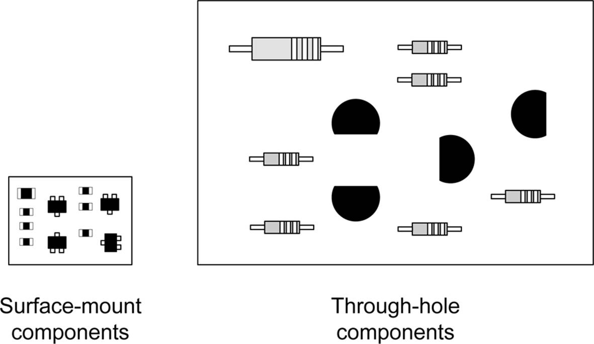
Figure 9-5. Comparison of surface-mount versus through-hole circuit boards
The surface-mount PCB in Figure 9-5 is a fraction of the size of the conventional through-hole board. If the through-hole PCB is 1 inch wide by 2 inches long, the SMT PCB is about 1/3 inch wide by 1/2 inch long. Granted, this is a somewhat contrived example (there are no connection points on the PCBs, for example), but it does show the relative size difference possible with surface-mounted components as opposed to conventional through-hole types. “Surface-Mount IC Package Types” covers surface-mount packages for ICs.
Using Different Package Types
Note that it is always a good idea to use the manufacturer’s datasheet dimensions when you’re laying out a PCB or sizing a part for a design. Don’t blindly trust whatever a PCB layout CAD package might have in its parts library, because there can be variations between manufacturers and even from year to year from the same source. For more about PCB layout, see Chapter 15.
In the following sections, each type of part has a description of the package types available, so we won’t go into any more details here. The primary point is to gain an appreciation for just how small things can get when surface-mount devices are used. The downside is that they can be extremely difficult to work with, and the investment required to obtain the necessary tools and supplies is not trivial.
Diodes and Rectifiers
Diodes and rectifiers are semiconductor devices that only allow current to flow only in one direction. Both types of devices have the same behavior, so the distinction arises from how they are used. Diodes typically deal with small amounts of current, while rectifiers are designed to handle large (sometimes very large) currents. Rectifiers are commonly used to convert the AC from a transformer connected to 120 VAC house current to DC that can then be filtered and regulated into DC for electronic devices. Diodes are typically used to rectify signals, restrict current flow, and limit signal levels, and in applications like video switching circuits and digital logic. A diode will typically respond to a change in current more quickly than a rectifier. This is called the switching time of the device. Appendix A provides some details about how the semiconductor junction in a diode or rectifier works, and Figure 9-6 shows graphically what happens when an AC signal encounters a rectifier.
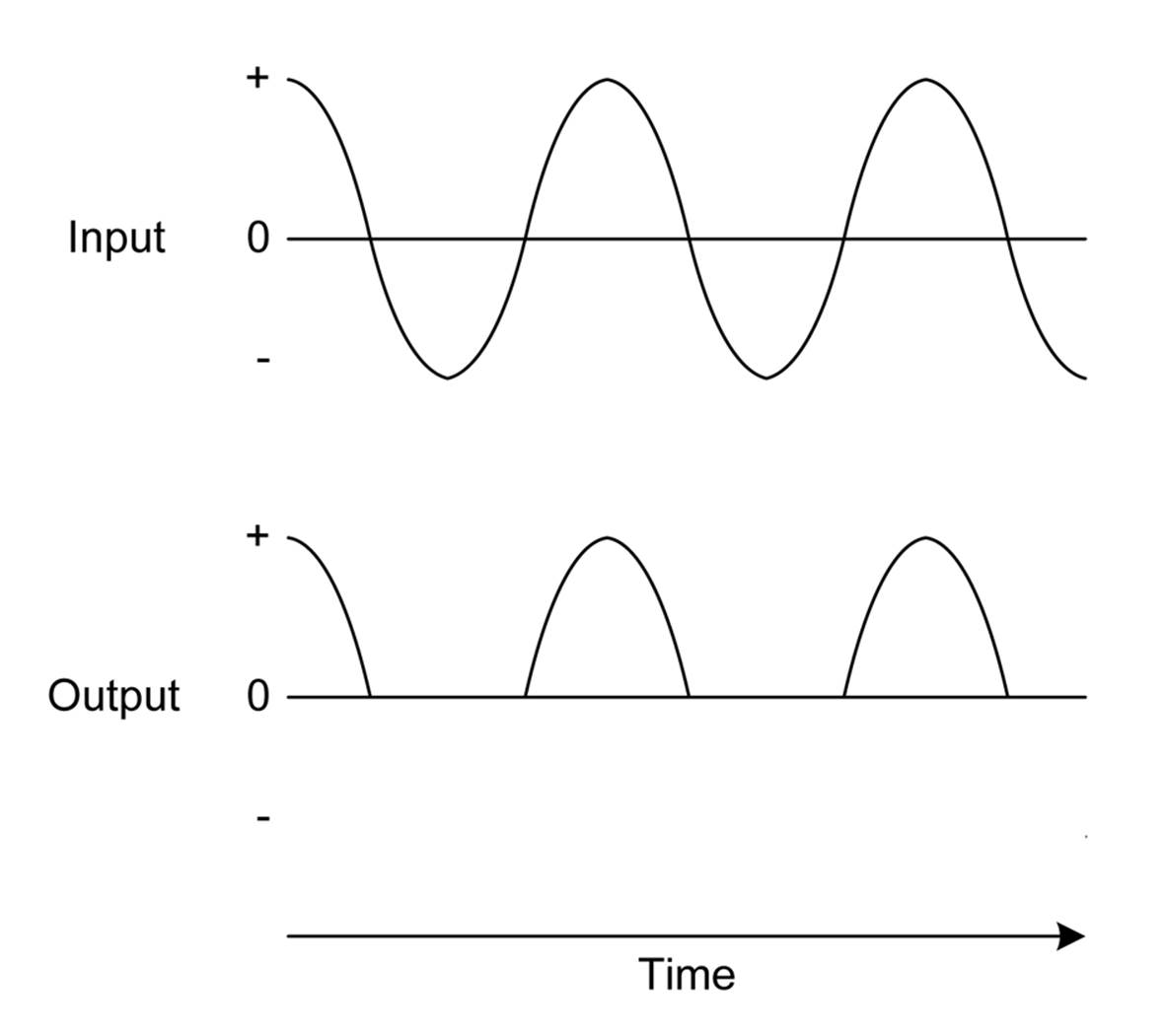
Figure 9-6. Conversion of AC to DC via rectification
Rectifiers have been around in one form or another for well over 100 years. Early rectifiers (late 1800s, early 1900s) used mechanical components such as vibrating armatures to rectify AC and convert it to DC. These were replaced by vacuum tubes in the early part of the 20th century, and also by rectifiers that were based on stacks of either selenium or copper oxide wafers. These early rectifiers tended to be large, bulky, and sometimes dangerous.
An early form of small-signal diode was the so-called cat’s whisker used in some simple radio circuits. It was invented around the same time as vacuum tube rectifiers, but, outside of some kits and specialty applications, it was obsolete by the 1920s. This device typically used a crystal of galena (the crystal form of lead sulfide) and a wire “whisker” that could be moved around on the face of the crystal to find the best location to rectify a radio signal. In other words, these were the original crystal radios. Literally.
The solid-state diodes and rectifiers we know today became common with the advent of silicon and germanium-based semiconductors. Modern rectifiers and diodes employ a solid-state junction, and they can be fabricated directly onto a silicon wafer as part of an integrated circuit.
Some devices have behaviors similar to common rectifiers but also have characteristics that make them uniquely suited for certain applications. Among these are Zener diodes, light-emitting diodes (LEDs), and photo-sensitive diodes. Of course, there are even more exotic types available, but we won’t delve into those, as their applications tend to be highly specialized. If you are curious, I encourage you to search out technical data on these exotic components, as some of them are quite fascinating.
Some parts are marked with a number printed on the body, while others have no markings at all except for the cathode band. For this reason, it is a good idea to keep diodes and rectifiers separate in small containers or envelopes with the part number written or taped to it. If they get jumbled, the only good way to sort them out is by using a test instrument called a curve tracer. While it’s not hard to build a workable curve tracer from junk parts and an old oscilloscope, it’s a chore that you can avoid by taking care to keep things neat and organized from the outset.
Small-Signal Diodes
Small-signal diodes, as the name suggests, are used to rectify low-voltage, low-current signals. Some types are extremely fast, making them suitable for use in radio frequency circuits or in some types of high-speed logic circuits. In fact, early computers used large numbers of small-signal diodes in their circuits. These served as early forms of read-only memory, among other things.
Figure 9-7 shows a typical small-signal diode in a glass package.
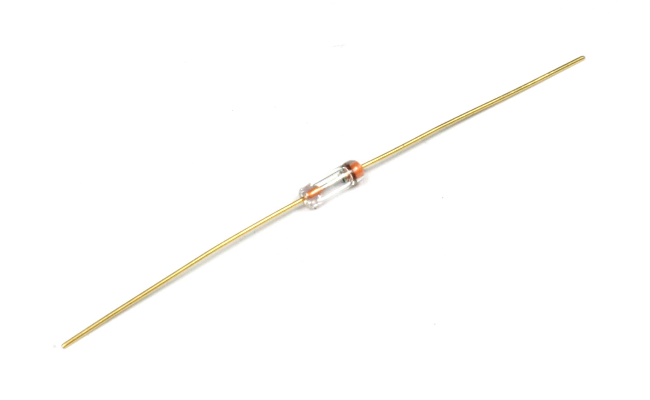
Figure 9-7. Typical small-signal diode
The JEDEC standard specifies that diodes use part numbers beginning with “1N.” In the case of Figure 9-7, this is a 1N4148 part, which is common. It has largely replaced the earlier 1N914 diode for most small-signal applications.
Diodes are rated in terms of forward voltage, peak inverse voltage, switching time, and forward current::
Forward voltage
Also referred as the forward bias, the voltage potential applied to a solid-state P-N junction that will result in current flow through the junction.
Forward current
The maximum amount of current that the P-N junction can safely carry when it is conducting while forward biased.
Peak inverse voltage (PIV)
The maximum reverse polarity voltage the P-N function can withstand before it breaks down and destroys the device. Note that avalanche and Zener diodes are designed to take advantage of reverse bias.
Switching time
The amount of time required for the P-N junction to transition between non-conducting to conducting states.
Table 9-1 gives the typical specifications for a 1N4148 diode. These are the primary things to note when you are examining the datasheet of a small-signal diode or selecting parts from a distributor’s parametric selection table.
|
Parameter |
Value |
|
Forward current (continuous) |
300 mA |
|
Forward voltage (typical) |
0.7V |
|
Peak inverse voltage |
75V |
|
Switching time (typical) |
4 nS |
|
Table 9-1. Essential 1N4148 specifications |
|
Note that the forward voltage will manifest as a voltage drop when the diode is in a circuit, and different diode types have different voltage drops. For a garden-variety red LED, the voltage drop is typically around 1.4V. Figure 9-8 shows how this would appear in a simple circuit.
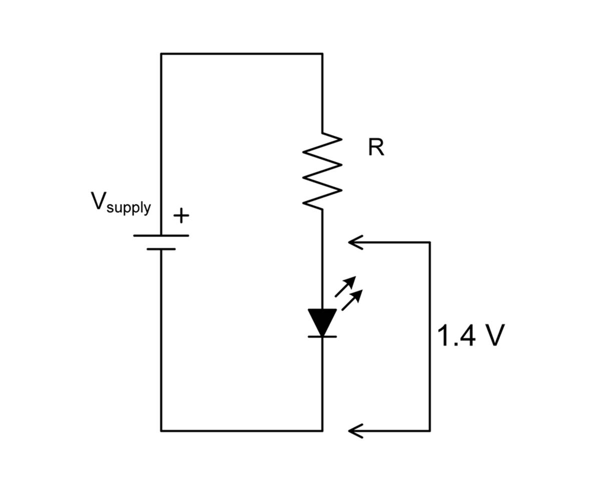
Figure 9-8. Voltage drop across an LED
The value of R in Figure 9-8 would be chosen to provide sufficient forward current to cause the LED to emit light, which can vary from manufacturer to manufacturer. Note that this is essentially a voltage divider, like the one described in Chapter 1. The same math would be used here to determine the value of R.
Rectifiers
A solid-state rectifier is useful for dealing with current flow of any significance, on the order of 500 mA or greater. They are typically used for AC rectification in power supplies, in protection circuits, and in voltage regulator circuits.
Figure 9-9 shows a IN4004 type rectifier, which is a 1A device capable of handling up to 400V of reverse voltage. It is common in small linear power supplies. Other members of the 1N4000 series have PIV ratings from 50 to 1,000 volts, and all are rated at 1 A of forward current.
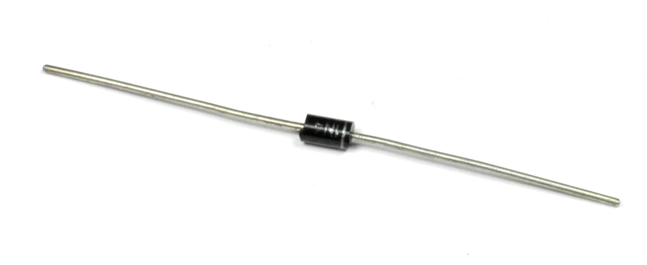
Figure 9-9. Typical small solid-state rectifier
Rectifiers come in packages other than axial lead types like the one shown in Figure 9-9. High-current rectifiers are available in so-called stud-mount packages, like the one shown in Figure 9-10.
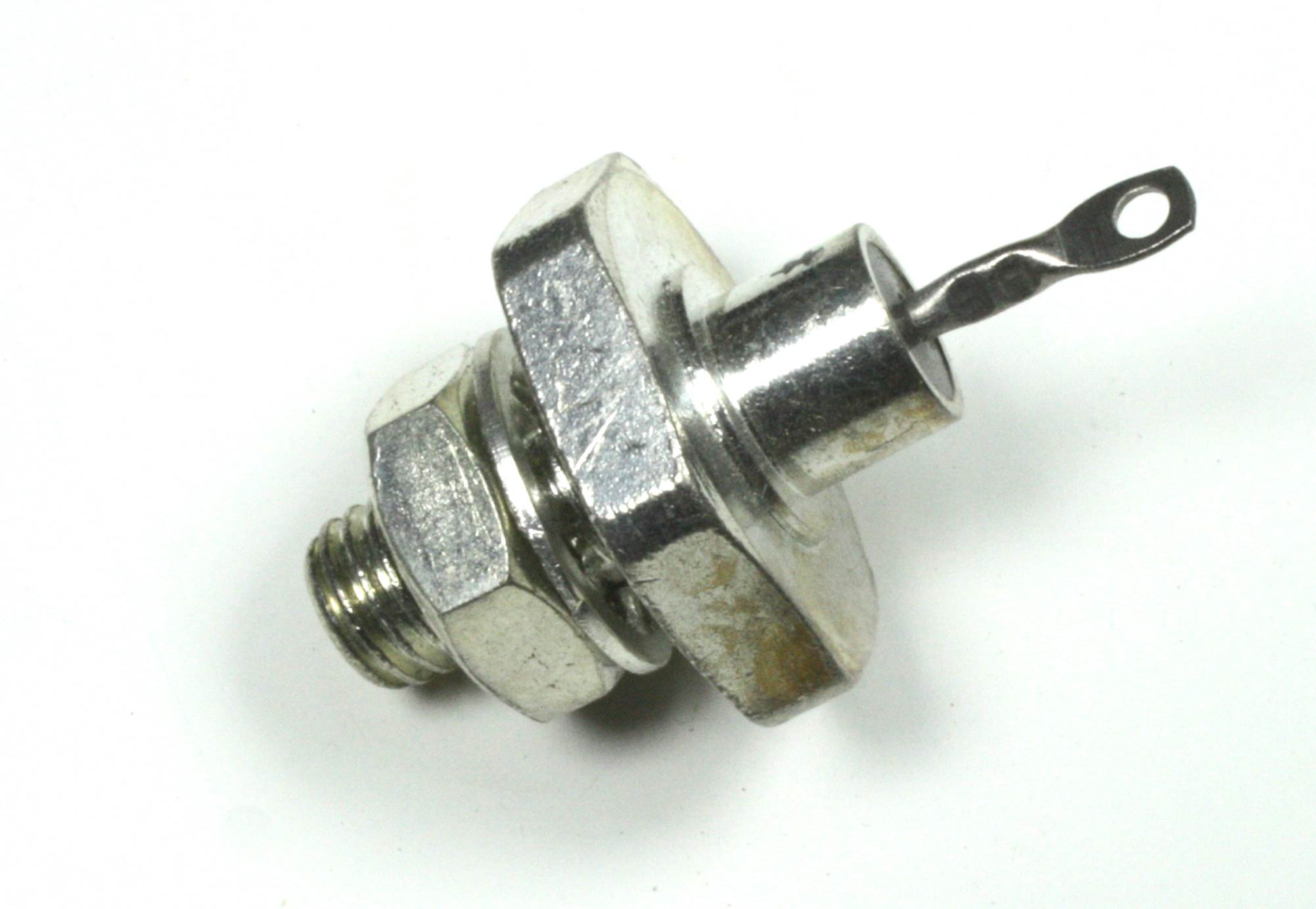
Figure 9-10. A stud-mounted rectifier
Yet another variation on the rectifier theme is the bridge rectifier. A bridge rectifier is a full-wave rectifier; that is, whereas a single rectifier will convert an AC signal to a pulsed DC signal (as shown in Figure 9-6), a full-wave rectifier will convert both the positive and negative parts of the AC signal to DC output, as shown in Figure 9-11.
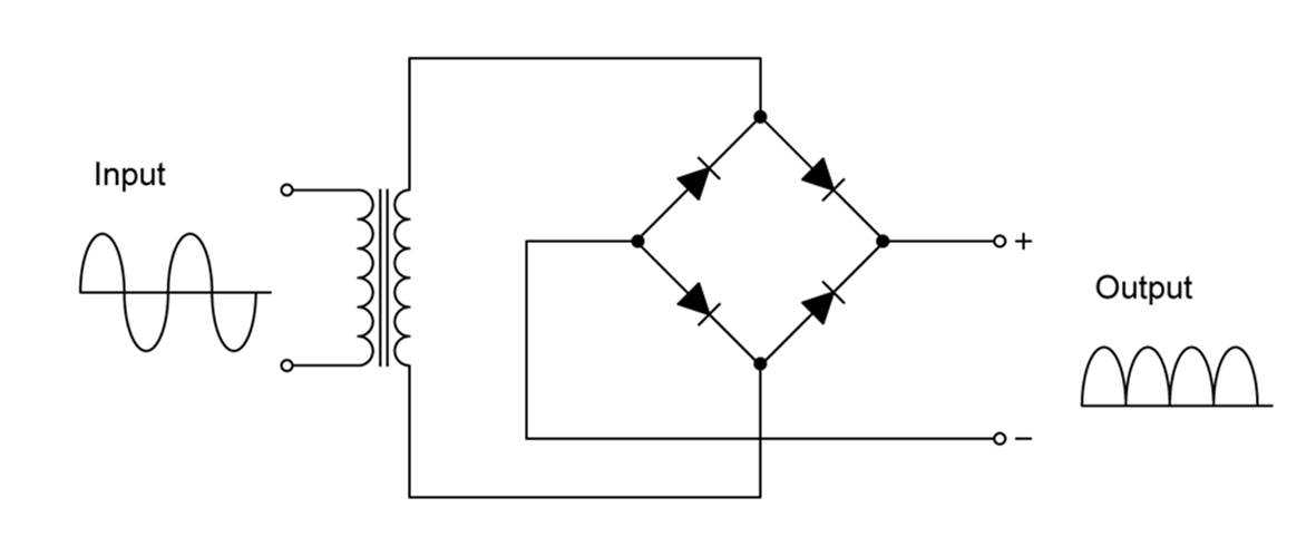
Figure 9-11. Full-wave rectification
Another variation of a full-wave rectifier circuit uses only two rectifiers, but it requires a center-tapped secondary winding on the transformer to serve as a common return. The full-wave bridge does not require the center tap. Figure 9-12 shows a small bridge rectifier. Larger types, with a center hole for mounting to a chassis or heatsink, are also available.
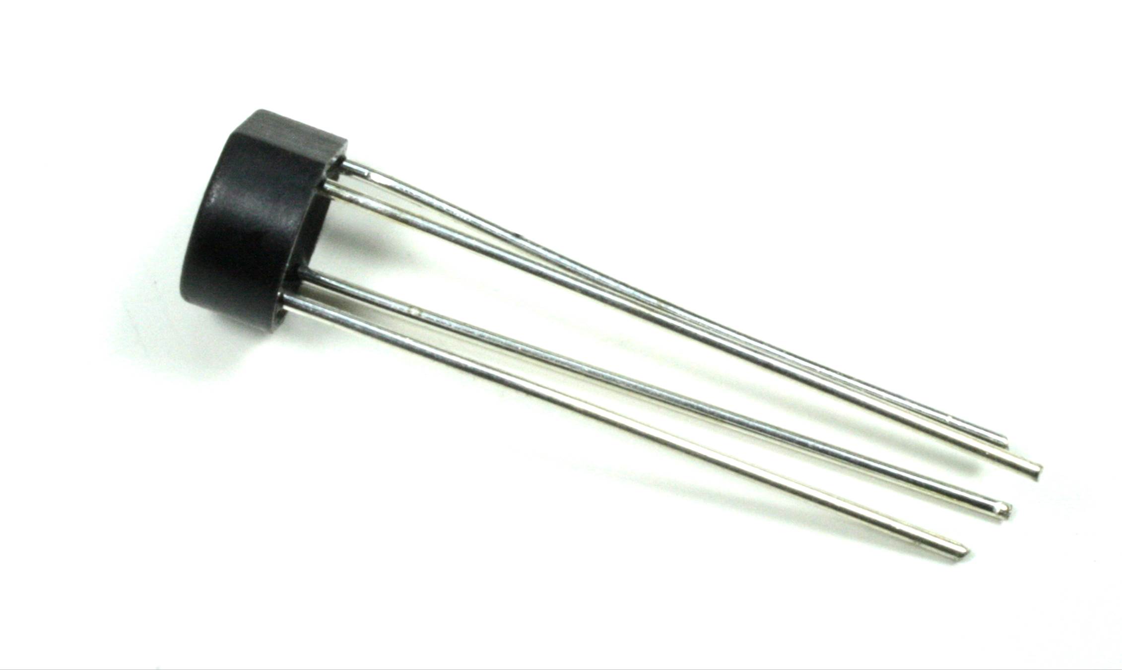
Figure 9-12. A small bridge rectifier
A small full-wave bridge, or even just four rectifiers, can be used to create a “don’t care” DC input for a circuit, as shown in Figure 9-13. Instead of an AC source like a transformer, if the input is a DC source, the rectifiers in the bridge will ensure that the output will always be consistent with regard to positive and negative. Although this trick isn’t commonly used, some devices do employ it. Some devices that use a wall transformer can accept either AC or DC input at the nominal voltage and work just fine because there is a full-wave bridge inside, and probably a voltage regulator and some filtering as well.
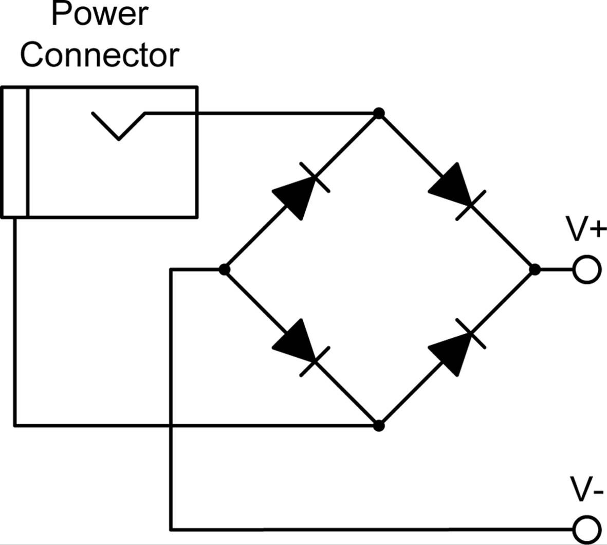
Figure 9-13. A “don’t care” DC power input protection circuit
Light-Emitting Diodes
A light-emitting diode is a type of rectifier that has been manufactured in a way that enhances its ability to produce light when current flows through the silicon junction at the heart of the device. This involves a process called doping, wherein specific impurities are added to the otherwise pure semiconductor material used in the device. Although all semiconductors have added impurities (otherwise, they wouldn’t work), an LED will generate light as a by-product of current flow.
LEDs come in a wide range of shapes, sizes, and output levels. Some types, designed for surface-mount applications, are very small, while others are large enough to be used for illumination purposes. LEDs also come in a variety of colors. The first LED components emitted light in the infrared. These were followed in the 1950s by devices that emitted visible red light. In the 1970s, yellow and green LEDs appeared. Blue LEDs didn’t appear until 1994, when Japanese researcher Shuji Nakamura demonstrated a high-output blue device. These days, you can purchase LEDs that emit light from infrared to long-wave ultraviolet. Figure 9-14 shows a selection of various types of LEDs.

Figure 9-14. A sample of various LED types
Because the core of an LED is basically just a small piece of semiconductor, the outer casing can be molded into almost any reasonable shape. In addition to those shown in Figure 9-14, cylindrical and arrowhead shaped packages are also available. These “oddball” shapes sometimes find their way into consumer electronics.
An LED is primarily characterized by its output wavelength (color), forward voltage, and forward current. The forward voltage is the voltage at which the semiconductor junction in the LED will start to conduct, and the forward current is the current at which the LED will produce its maximum output. The lowest common forward voltage is 1.6V, and some low-current devices will glow with only 1 mA. Other devices have a forward voltage as high as 14V and a current of 70 mA.
Zener Diodes
A Zener diode is a device that behaves in many respects like a typical diode. Physically, Zener diodes look identical to any other diode or rectifier. What sets a Zener apart is that, when the current is reversed, it will not allow the current to pass until a specific voltage level is reached. When this occurs, the Zener will conduct in the reverse direction.
This unique characteristics allow Zener diodes to be used as a form of voltage regulator, and they are often used to produce a reference voltage. A Zener with a rating of, say, 5.1V, can be used to shunt any voltage greater than 5.1V to ground. Anything less than 5.1V will not be affected.
Exotic Diodes
A solid-state silicon junction is sensitive to external energy, such as heat and light. This sensitivity can be enhanced to create a device that is useful as a light sensor. A PIN diode (the name refers to the P-I-N junction in the device, where the I stands for Indium) has a modified junction between its semiconductors. When used as a light detector, a PIN diode is connected in reverse such that no current flows until a photon strikes the junction. When this happens, the junction temporarily conducts and allows current to flow.
Solid-state lasers are a variation on the LED, but with some structural modifications to make it possible for the device to emit coherent light. Laser diodes are connected to a circuit much like an LED, and their output can be modulated to carry information. They are useful for fiber-optic communications systems, and infrared versions are used in military applications for target designation. They are also commonly used as pointers to annoy people at meetings and for teasing pets with a bright spot they can’t catch. Figure 9-15 shows a module that can be used with something like an Arduino.
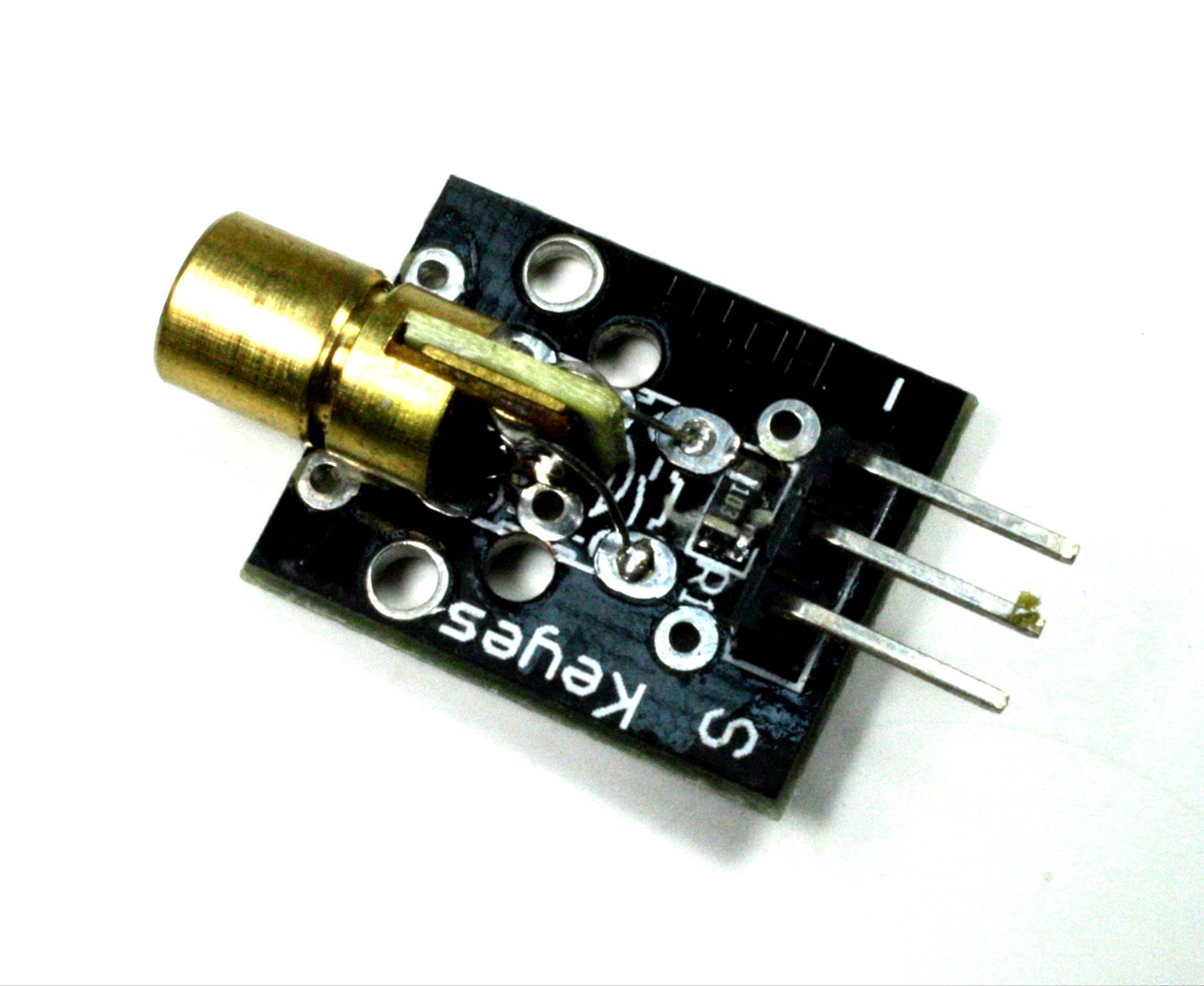
Figure 9-15. Small laser-diode module
Laser diodes are available in output powers ranging from around 5 mW up to and beyond 30W. The low-power types are commonly found in laser pointers, whereas higher power parts, in the 500 mW to 800 mW range, are used in CD and DVD drives. Devices with output powers above 1W are used in engravers, cutters, labeling systems for date codes, and some projection systems.
Diode/Rectifier Axial Package Types
Axial packages for discrete diodes and rectifiers with axial leads are defined by a series of type numbers beginning with a DO prefix in the DO-204 family defined by JEDEC. The DO-35 package is commonly used for small-signal devices, and the DO-41 package is used with larger devices, such as the 1N4004 rectifier. Use the outline drawing in Figure 9-16 when looking at Table 9-2.
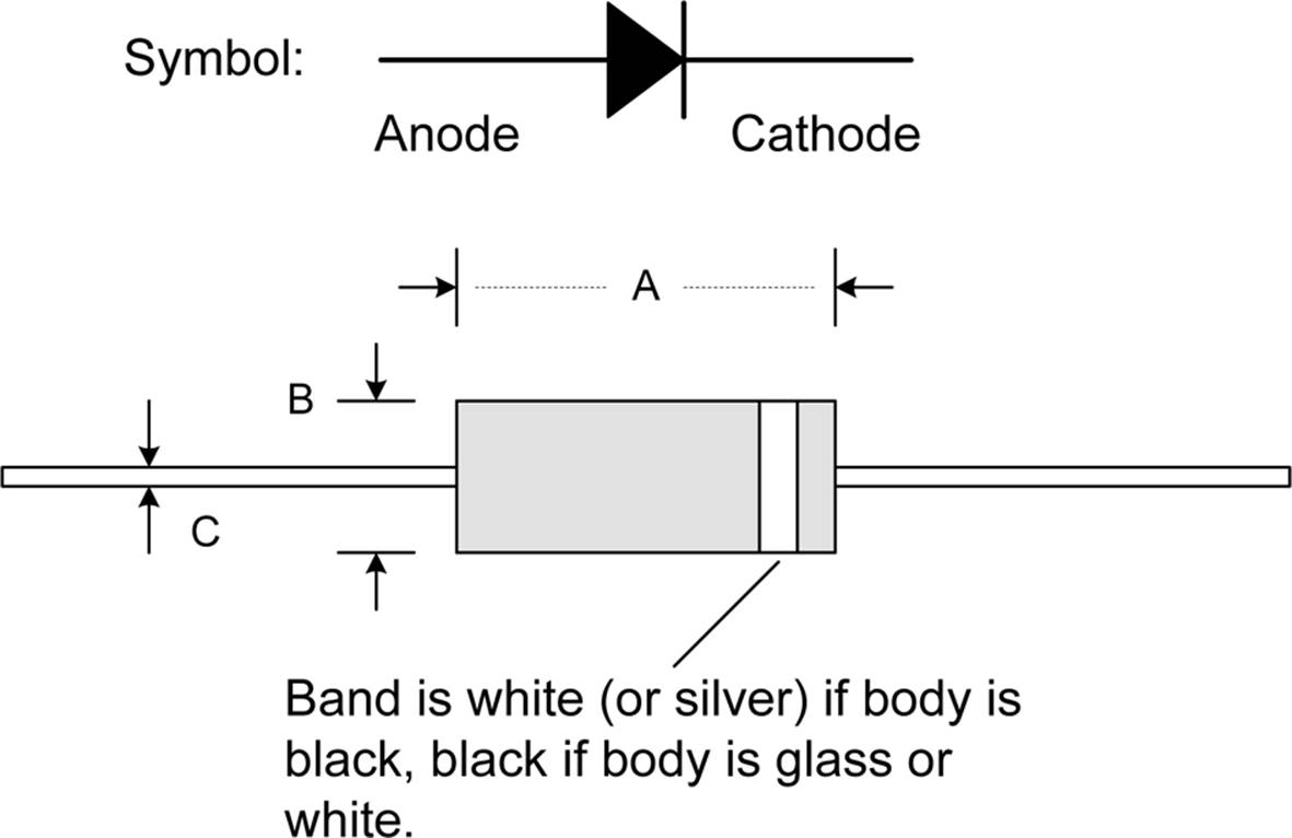
Figure 9-16. Axial-lead diode package dimensions
Semiconductor schematic symbols typically use an arrowhead to indicate conventional current flow through the device. As discussed in Chapter 1, the conventional current flow is the opposite of how the electrons in a circuit move. In the case of diodes, this means that the terminal names (cathode and anode) have the meaning you might expect, in that electrons enter through the cathode, move across the semiconductor junction, and emerge at the anode. There is current flow when the cathode is negative with respect to the anode. However, thanks to Ben Franklin and general social inertia, current flow is described as moving from the anode to the cathode. We just have to live with it and remember to switch our thinking around as the need may arise.
|
JEDEC |
A |
B |
C |
|
DO-16 |
2.54 |
1.27 |
0.33 |
|
DO-26 |
10.41 |
6.60 |
0.99 |
|
DO-29 |
9.14 |
3.81 |
0.83 |
|
DO-34 |
3.04 |
1.90 |
0.55 |
|
DO-35 |
5.08 |
1.90 |
0.55 |
|
DO-41 |
5.20 |
2.71 |
0.86 |
|
Table 9-2. Standard JEDEC axial diode package dimensions1 |
|||
Diode/Rectifier Surface-Mount Packages
Diodes and rectifiers are available in surface-mount packages similar to those used for resistors and capacitors, and some employ the same package numbering system (see Chapter 8). Some have metalized ends for soldering. Larger packages, such as the DO-214, employ folded leads.Figure 9-17 shows three different surface-mount package types for diodes-type devices. The upper set of numbers is the minimum size, the lower set is the maximum, and numbers in parentheses are millimeters.
There are many other package types besides the ones shown in Figure 9-17. Note that, while not shown in the figure, the packages have markings to indicate which end is the cathode and which is the anode. As always, be sure to consult the datasheet for the specific dimensions and devicecharacteristics.
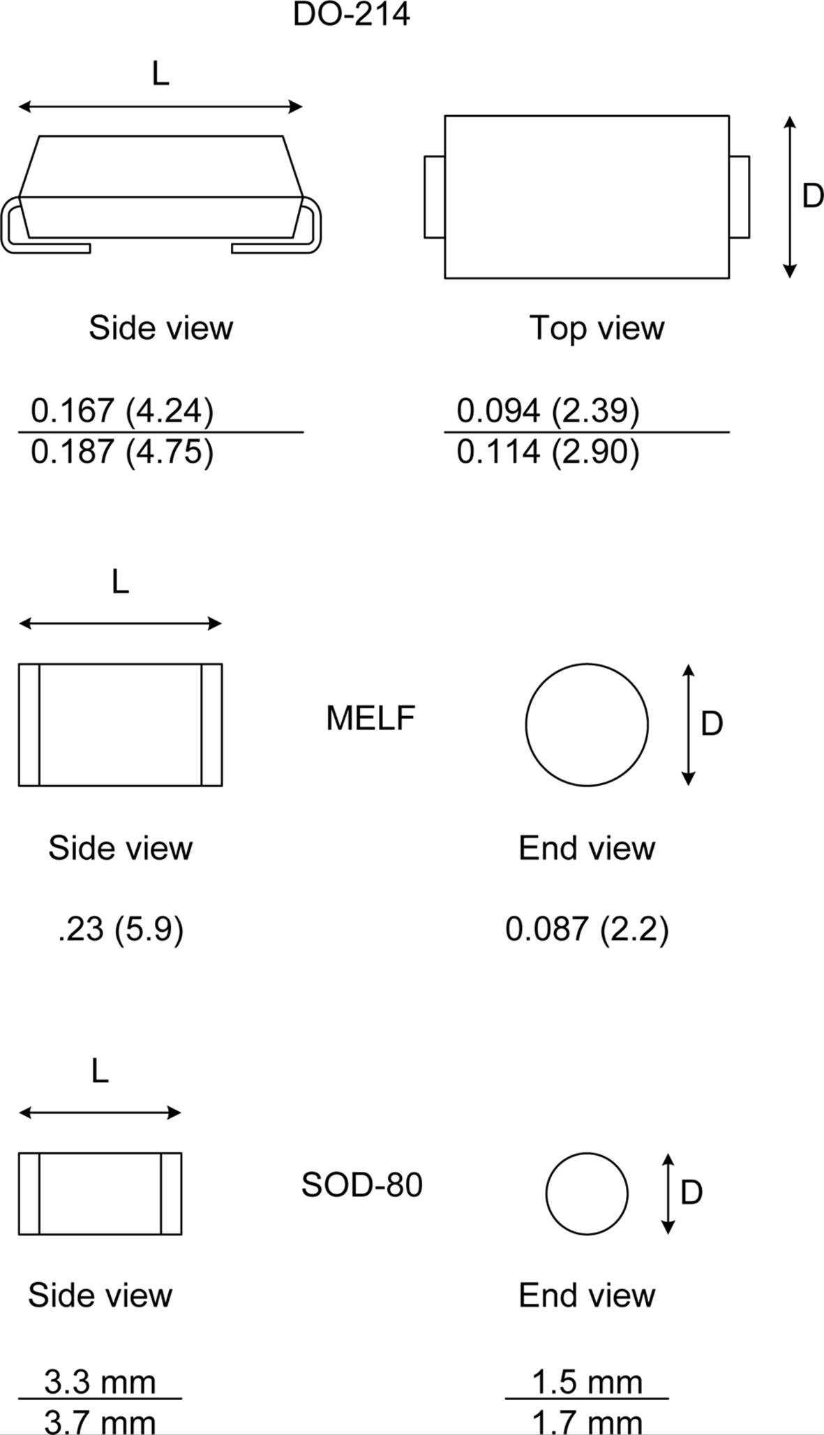
Figure 9-17. Examples of surface-mount diode and rectifier packages
LED Package Types
LEDs come in a variety of physical forms, from the common radial lead types like those shown in Figure 9-14, to minuscule surface-mount parts, jumbo-size devices used for lighting and electronic sign applications, and metal-enclosed laser diodes like the one shown in Figure 9-15.
In addition to round shapes in various diameters, LEDs are also available in rectangular shapes, such as the styles shown in Figure 9-18. The T1 standard lamp size is another popular form factor, with a diameter of 3 mm and an overall body length of 5 mm. Many 3 mm size LEDs are interchangeable with T1 type bulbs.
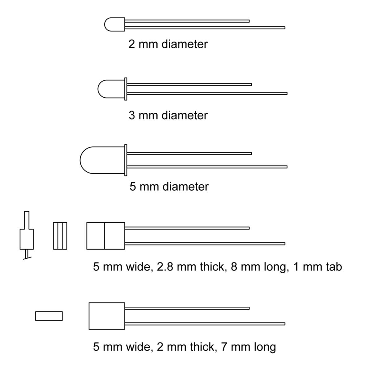
Figure 9-18. A small sample of available LED shapes
LEDs are available in surface-mount packages as well as through-hole types. The 0603 and 0805 sizes are popular (see Chapter 8 for a description of standard surface-mount package sizes), and kits containing a variety of colors are available for about $12 from distributors such as Digikey (see Appendix D). Figure 9-19 shows an outline drawing of a Dialight 598 series LED in an 0603 package.
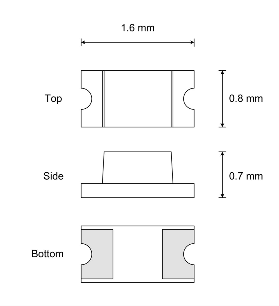
Figure 9-19. A Dialight 598 series 0603 package surface-mount LED
Other sizes are also available, from 0402 (1005 metric) to 1616. Side-looking packages allow surface-mount LEDs to be mounted such that they are visible at a 90-degree angle to the surface of the PCB.
Transistors
In 1947, the world’s first transistor was created at AT&T’s Bell Laboratories, and the world underwent some massive changes as a result. These early devices used germanium as the semiconductor, and they tended to be fragile and expensive. In 1954, the silicon transistor appeared, followed in 1960 by metal-oxide semiconductor (MOS) devices.
Transistors can be classified into two basic types: bipolar junction and field-effect. Bipolar junction transistors (BJTs) have unique operating characteristics quite unlike any other electronic component. Transistors can be used as amplifiers, regulators, or switches. In truth, the regulator application is closely related to high-power amplifiers, although most people probably don’t think of a power supply that way. When used as switches, transistors formed the basis of the first solid-state logic circuits in computers, with later, and faster, devices finding applications in radio communications and radar systems. BJT devices are fabricated as either NPN or PNP. This refers to the type of semiconductors used to create the device and the order in which they are arranged internally. Appendix A discusses semiconductor junctions in more detail, and the texts listed inAppendix C have even more detail.
A field-effect transistor can be either an N-channel or P-channel device, depending on how it was made. FETs also come in a number of variations, from the original type to more modern MOSFET designs. Each type has its own unique set of characteristics, such as current handling capacity, voltage range, and switching speed, that make it suitable for a particular application.
Figure 9-20 shows the schematic symbols for both NPN- and PNP-type BJTs. Appendix B contains a comprehensive set of schematic symbols, including various types of transistors. Refer to Appendix A for an overview of solid-state concepts.
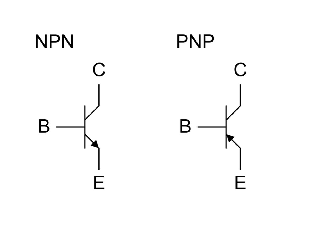
Figure 9-20. Standard schematic symbols for BJT transistors
The letters B, C, and E refer to the names of the terminals on a BJT device. These are base, collector, and emitter, respectively. In a BJT, current flows between the E and C terminals, and the B terminal acts as the control input.
Small-Signal Transistors
Just as with small-signal diodes, a small-signal transistor is designed to work with low voltage and current levels. Small-signal transistors come in a variety of package styles, from surface-mount to multi-legged metal cans. Figure 9-21 shows a selection of package styles available.
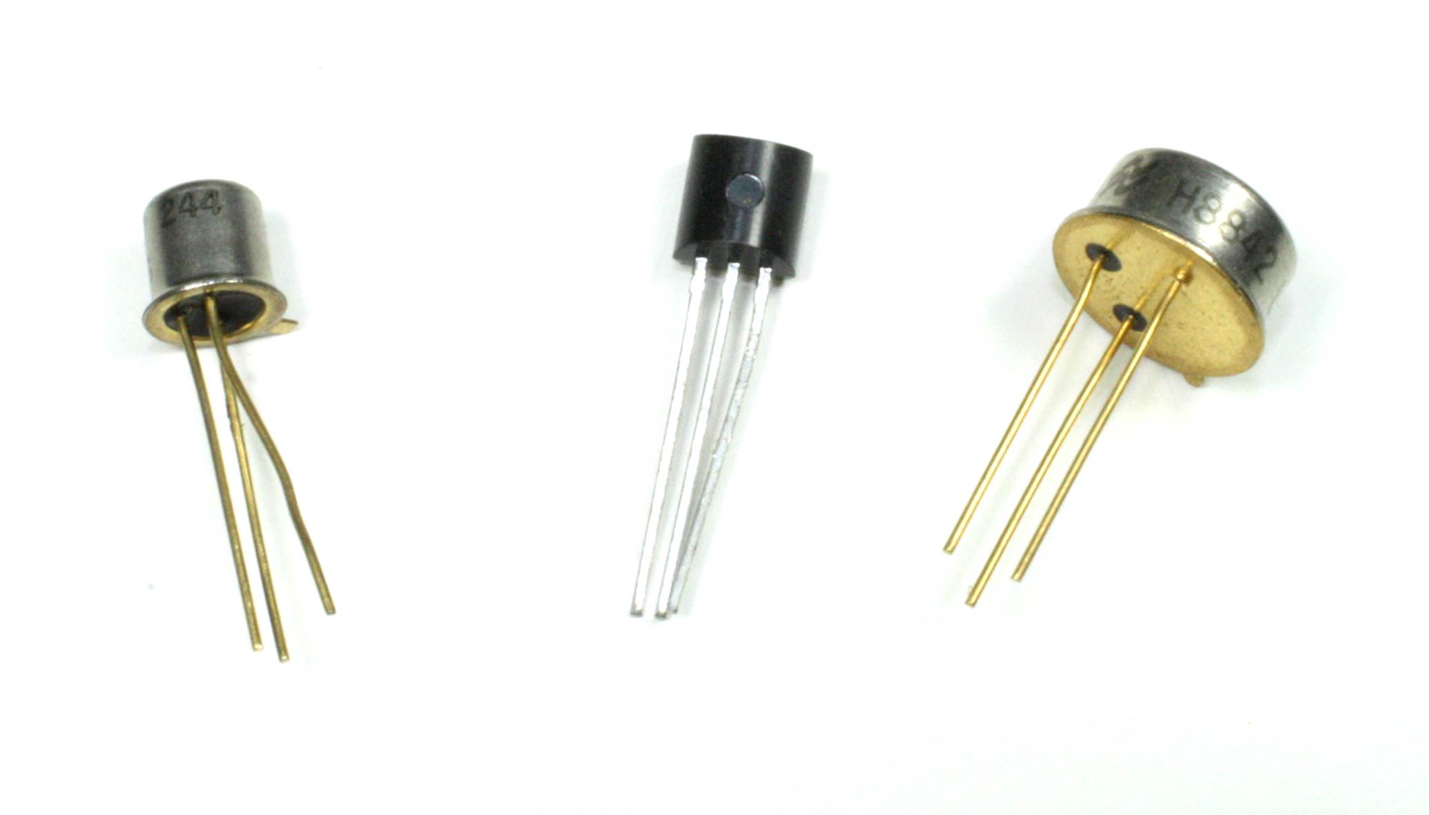
Figure 9-21. Assortment of small-signal transistors
A selection of inexpensive small-signal transistors is handy to have around. Table 9-3 lists some types that are useful for switching, controlling low-current relays, and driving LEDs, and as amplifiers and oscillators. PN2222 (plastic TO-92 package) parts can be purchased for as little as 10 cents each from companies such as Alltronics (see Appendix D).
|
Number |
Type |
Vce |
Ic |
Pd |
Ft |
Packages |
|
2N2222 |
NPN |
40 V |
800 mA |
500 mW |
300 MHz |
TO-92, SOT-23, SOT223 |
|
2N2907 |
PNP |
60 V |
600 mA |
400 mW |
200 MHz |
TO-92, SOT-23, SOT223 |
|
2N3904 |
NPN |
40 V |
200 mA |
625 mW |
300 MHz |
TO-92, SOT-23, SOT223 |
|
2N3906 |
PNP |
40 V |
200 mA |
300 mW |
250 MHz |
TO-92, SOT-23, SOT223 |
|
Table 9-3. Listing of low-cost small signal transistors |
||||||
The parameters used in Table 9-3 are defined as follows:
Vce
Maximum voltage across collector and emitter
Ic
Maximum current at the collector
Pd
Maximum device power dissipation
Ft
Maximum usable frequency
Power Transistors
As you might guess, a power transistor is designed to handle significant amounts of current, from several hundred milliamps to over 100 amps or more. Today, it is more common to see MOSFETs in the role of power transistors rather than BJT devices, mainly because the MOSFET can operate more efficiently at high power and voltage levels than the BJT type. Refer to “Field-Effect Transistors” for more on FET devices.
Figure 9-22 shows some of the package options available. Notice that each type is designed to be mounted onto something, such as a panel or some other form of heatsink.
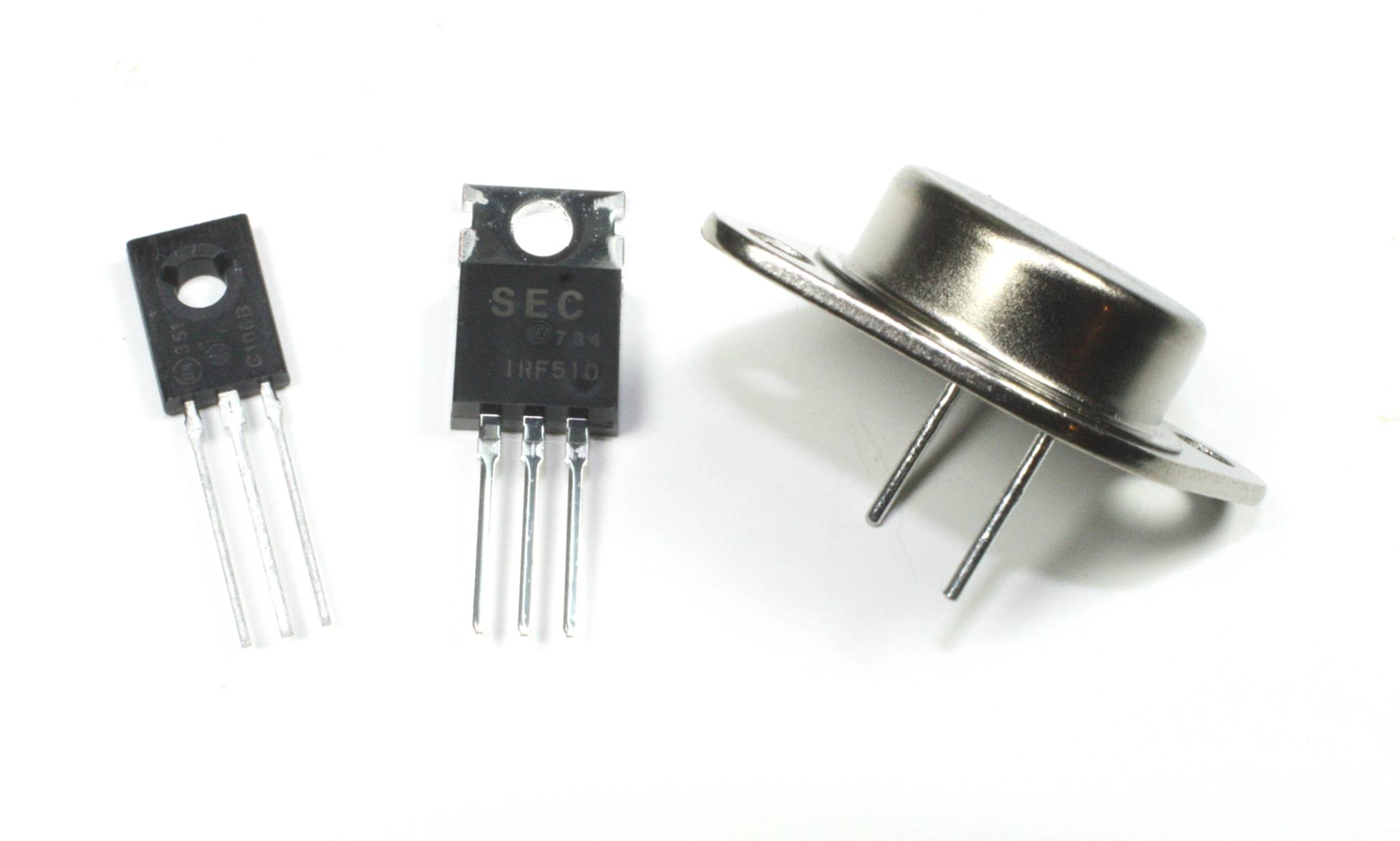
Figure 9-22. Assortment of power transistors
For most small projects, a power transistor is not necessary. But, should you ever need to control something like a high-current contactor, a heating element, or a hefty DC electric motor, a power transistor might be required.
Field-Effect Transistors
Whereas a BJT works by modulating the exchange of positive and negative charge carriers across a semiconductor junction, field-effect transistor devices behave in a manner similar to the operation of vacuum tubes. A FET controls the flow of electrons moving through its junction in proportion to the amount of voltage present on the gate pin of the device. In fact, there have been solid-state vacuum tube replacements made from high-voltage FET devices that plug in where a vacuum tube used to reside.
A MOSFET (which, as noted earlier, stands for metal-oxide semiconductor field-effect transistor) is a common type of FET. These devices have a low internal resistance when in the “on” state, and some types can handle a significant amount of current. They are often used in DC power switching circuits, and have also been put to use in the output stage of audio amplifiers. FET devices come in TO-3, TO-5, TO-92, TO-66, and TO-220 packages, as well as small-outline transistor (SOT) and other types of surface-mount packages.
Conventional Transistor Package Types
Transistors and other devices are packaged in a variety of styles, some of which have fallen into disuse over time as surface-mount technology has become more prevalent. But for some transistor types, a through-hole package is still the only feasible way to go, particularly if the device needs to be mounted on a heatsink of some sort. Radial lead parts are usually mounted directly on a PCB in an upright position.
Table 9-4 lists some of the transistor package types that are available. Some of these are shown in Figure 9-23, but not all, since some are now either considered obsolete or are uncommon, but you might still encounter them in the wild at some point.
|
Case |
Mounting |
Package type |
|
TO-3 |
Flange mounted |
Metal can |
|
TO-5 |
Radial leads |
Metal can |
|
TO-18 |
Radial leads |
Metal can |
|
TO-46 |
Radial leads |
Short metal can |
|
TO-52 |
Radial leads |
Metal can |
|
TO-66 |
Flange mounted |
Metal can |
|
TO-92 |
Radial leads |
Molded plastic |
|
TO-126 |
Flange mounted |
Plastic/metal |
|
TO-202 |
Flange mounted |
Plastic/metal |
|
TO-218 |
Flange mounted |
Plastic/metal |
|
TO-220 |
Flange mounted |
Plastic/metal |
|
TO-254 |
Flange mounted |
Plastic/metal |
|
TO-257 |
Flange mounted |
Metal can |
|
TO-264 |
Flange mounted |
Plastic/metal |
|
TO-267 |
Flange mounted |
Metal can |
|
Table 9-4. JEDEC transistor package types |
||
Transistors that are flange mounted usually require a flat surface of some sort, either a metal plate, chassis panel, or a heatsink. It is possible to simply solder a TO-126, TO-202, and TO-220 (and similar types) directly to a PCB if it won’t be dissipating very much power. Heatsinks are available for these types that attach to the mounting flange of the transistor, allowing it to stand free.
Figure 9-23 shows some examples of common transistor packages. Note that the TO-66 is essentially a smaller and slightly narrower version of the venerable TO-3 package.
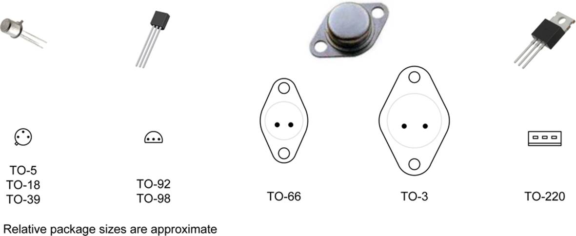
Figure 9-23. Common transistor package types
Transistor pin definitions can vary from one type to another and, of course, a FET or a TRIAC (triode for alternating current; discussed shortly) will have different connection types than a BJT device. Figure 9-24 shows pin connections for some common package styles. Note that these are just a small sample of the possible variations. Just because something is in a TO-18 package, don’t assume that it’s a BJT with the same E-B-C pin order as shown in Figure 9-24. The pins might be in a different order, or it might be a UJT (unijunction transistor) or a FET.
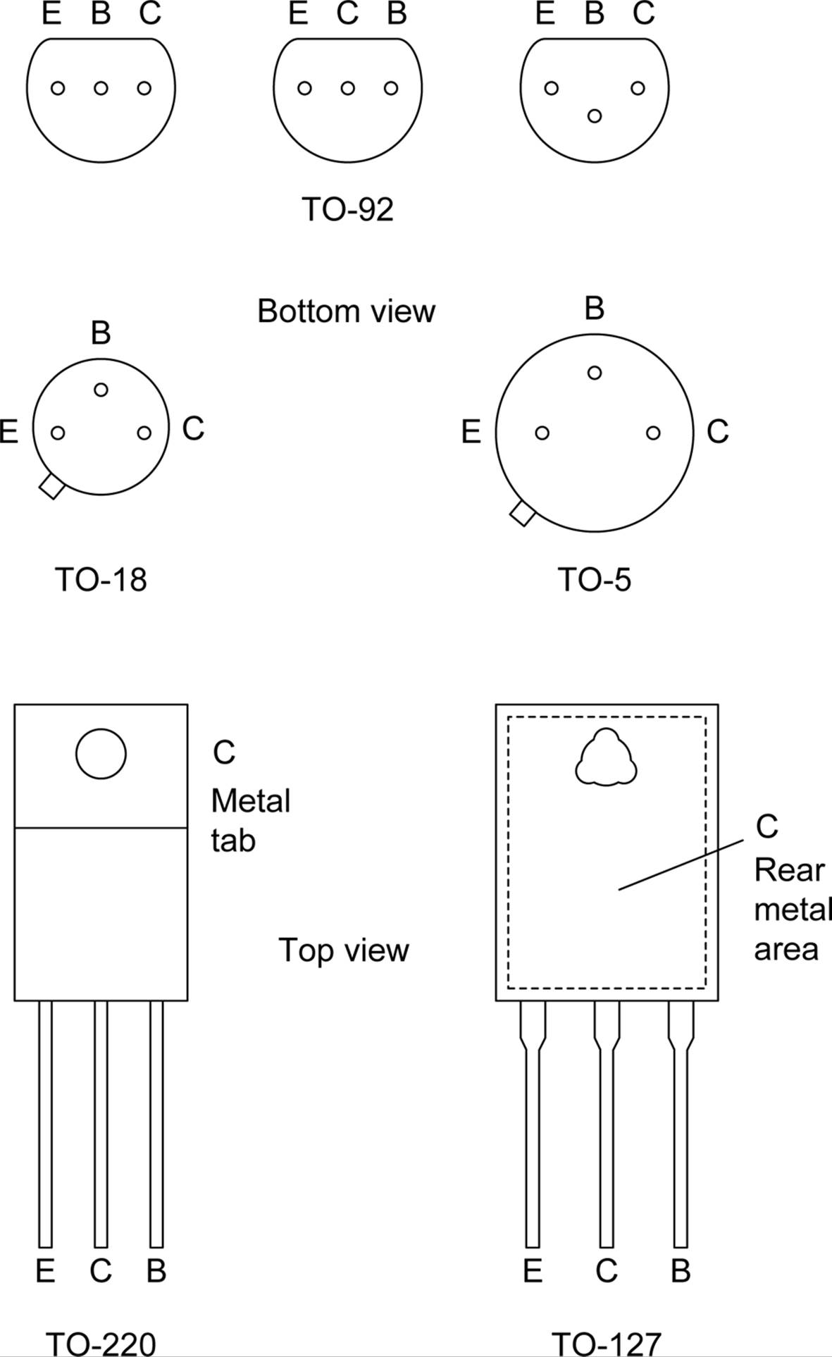
Figure 9-24. Common transistor pin connections
Refer to the datasheet, if possible, for the actual connections for a particular device. Often, a part purchased as a single item in a plastic retail display package will have the connection diagram on the package. If you have a part with no markings, or if it has a custom number assigned by the equipment manufactuer to prevent people from reverse-engineering their amazing technology, I would suggest discarding it. While it is possible to determine the basic characteristics of a BJT or a FET using test equipment, it’s really not worth the effort in many cases. If a part costs only 50 cents, your time is a lot more valuable. Just chuck it in the trash and purchase the right part.
Surface-Mount Transistor Package Types
SMD transistor packages typically have three connection points or leads for single device packages. Some parts might contain more than one transistor and consequently more leads. The SOT-23 (small-outline transistor, type 23) package, shown in Figure 9-25 with a couple of other common transistor package, is common.
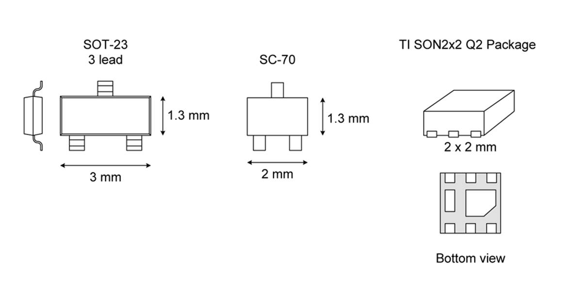
Figure 9-25. A selection of common surface-mount packages used for transistors
The SON2x2 package is used for a power MOSFET device, with the large area under the package being a heatsink connection.
Refer to the datasheet for the connections for a particular device. Most, but not all, SOT-23 and SOT-223 type packages use the arrangement shown in Figure 9-26. The SOT-223 is basically the surface-mount equivalent of the TO-220 shown earlier. The emitter pins are duplicated to accommodate the higher current capacity of the component. The SOT-223 package is also used with devices such as linear voltage regulators.
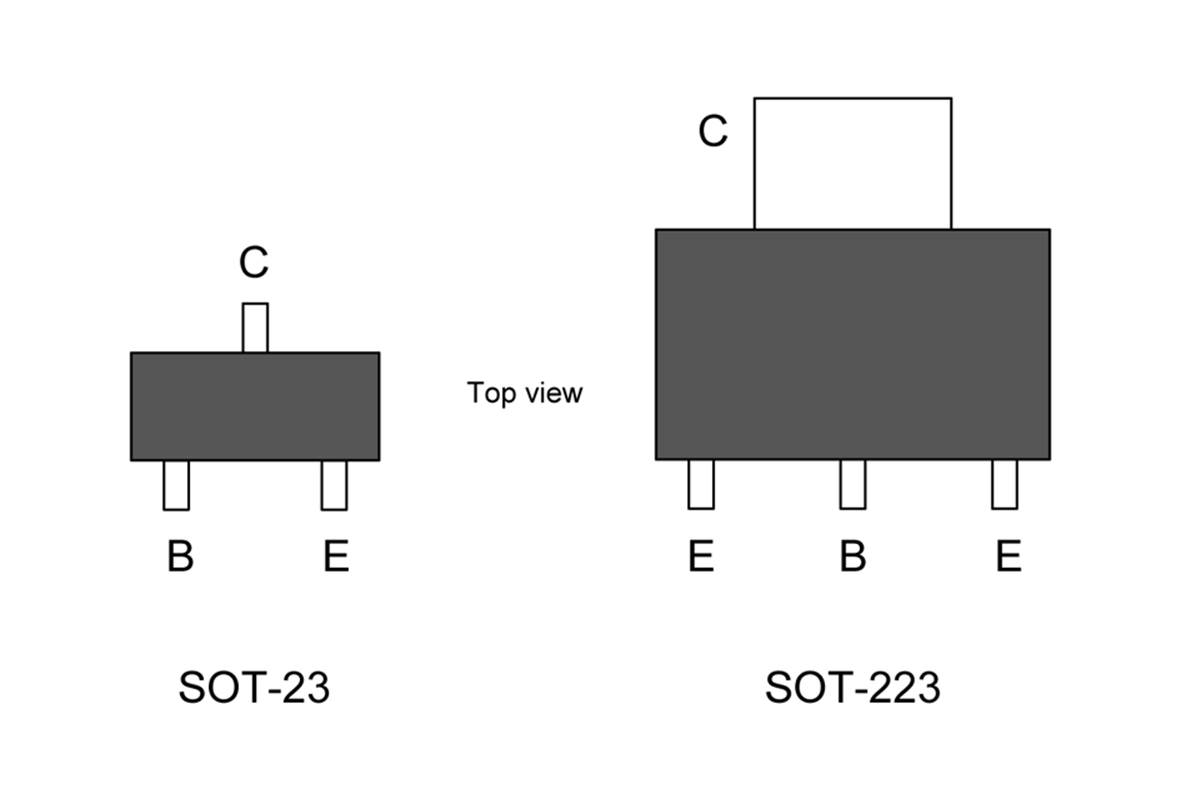
Figure 9-26. Pinout diagrams for the SOT-23 and SOT-223 packages
SCR and TRIAC Devices
SCRs (silicon-controlled rectifiers) and TRIACs (triodes for alternating current) are members of a class of solid-state active devices called thyristors. These are used exclusively for power control applications. Appendix B shows the schematic symbols used for SCR and TRIAC devices.
In terms of packaging, an SCR or a TRIAC looks a lot like a conventional transistor. The plastic TO-220 package is popular, and some devices with higher current capacity come in the TO-3 metal-can package. There are also small TO-5 and TO-92 versions, as well as some surface-mount types. Very high-power devices are available in stud-mounted packages, similar to the types used for rectifiers shown in Figure 9-10. The difference is that the SCR or TRIAC will have two terminal posts protruding from the body of the package instead of just one.
Silicon-Controlled Rectifiers
A silicon-controlled rectifier is a four-layer semiconductor that behaves like a gated diode and passes current in only one direction when it is enabled. It doesn’t conduct until a voltage is present on the gate terminal, after which it will continue to conduct until the current flow through the device drops close to zero (or some specific cut-off threshold). SCRs are available in different package styles, depending on the rated power capacity of a particular device. Low-current devices can be found in TO-92 packages, while higher current parts come in TO-220, TO-3, or stud-mount packages.
TRIACs
If you have a light dimmer in your house, chances are, you also have a TRIAC. Unlike an SCR, a TRIAC can pass current in both directions. Like the SCR, a TRIAC does not conduct until a voltage is applied to the gate terminal. Because of their ability to conduct in both directions, TRIACs are commonly used for AC power control by enabling current flow for only part of a positive or negative cycle. Appendix A shows an example of how a TRIAC is used to control AC current in a light dimmer using an RC phase shift circuit.
As with SCRs, TRIACs are available in a variety of packages. The TO-220 style is common, and high-power versions are available in TO-3 and stud-mounted packages.
Heatsinks
Solid-state components can get extremely hot during operation as heat builds up in the package of the device. Even though the current through a device might not exceed its rated maximum, or even come close to it, the device can be damaged if excessive heat is allowed to accumulate over time. Without some way to conduct the heat away from the part, it might eventually fail.
Power transistors are particularly susceptible to overheating, due to the amount of current they are capable of handling. One tried-and-true way to deal with the issue is to use a heatsink. Purpose-made heatsinks can be had for almost every power transistor package type, including the TO-202, TO-220, TO-66, and TO-3 styles. In many situations, the part is simply mounted to a panel, chassis, or other large metallic mass that can conduct heat away from the part. Insulating shims can be placed under the case of the transistor to isolate it, and nylon or phenolic fiber washers are typically used to isolate the mounting screws.
In other cases, there might be sufficient air flow to allow the part to mount directly to a freestanding heatsink, such as the TO-220 type shown in Figure 9-27. This type of heatsink is designed to stand vertically on a PCB with the transistor bolted to it. A thin layer of thermal conductive compound or a special thermal pad is sometimes placed under the body of the transistor between it and the heatsink to improve the thermal conductivity.
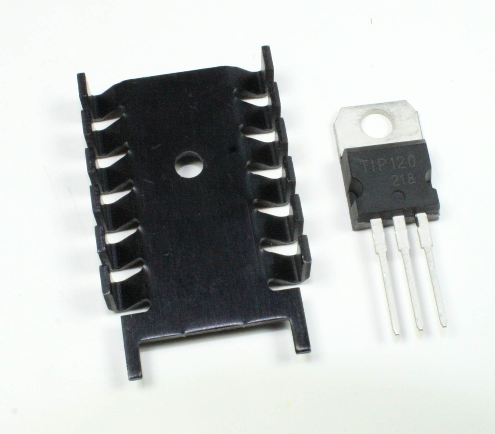
Figure 9-27. TO-220 vertical mount freestanding heatsink
There are similar styles available for the TO-66 and TO-3 packages as well. Since the heatsink isn’t physically connected to anything around it, there is no need to electrically insulate the body of the transistor, which simplifies mounting. Figure 9-28 shows how the transistor is aligned on the heatsink (although in this case the mounting hardware has been omitted for clarity).
Figure 9-29 shows a vertically mounted heatsink for a motor driver IC on a PCB. The part is similar to a TO-220, only it’s much wider to accommodate more pins. It is used as a motor controller, so it has to be able to deal with some significant amounts of current.
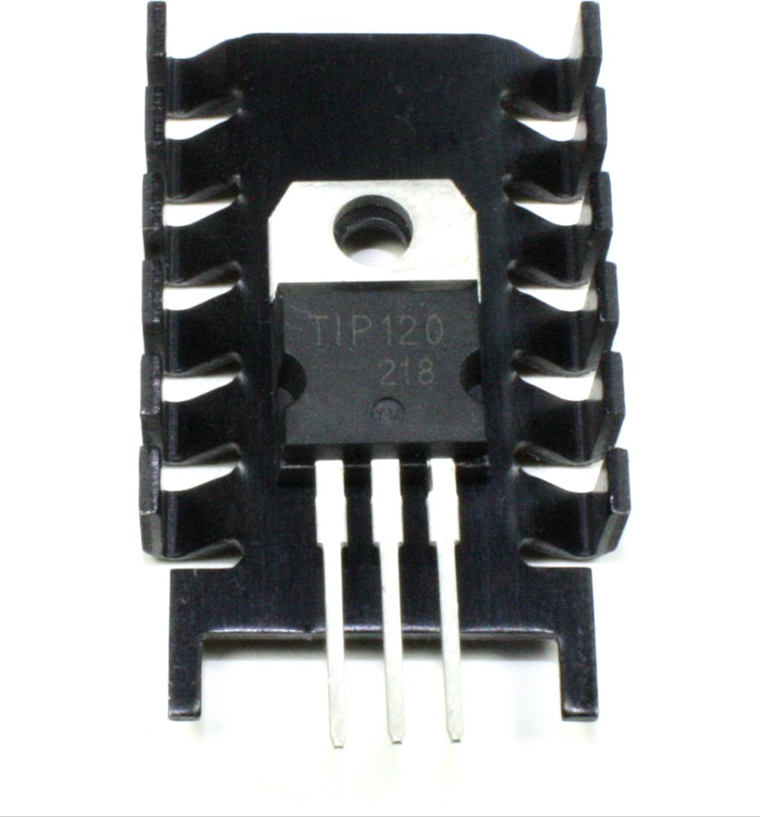
Figure 9-28. TO-220 on vertical heatsink
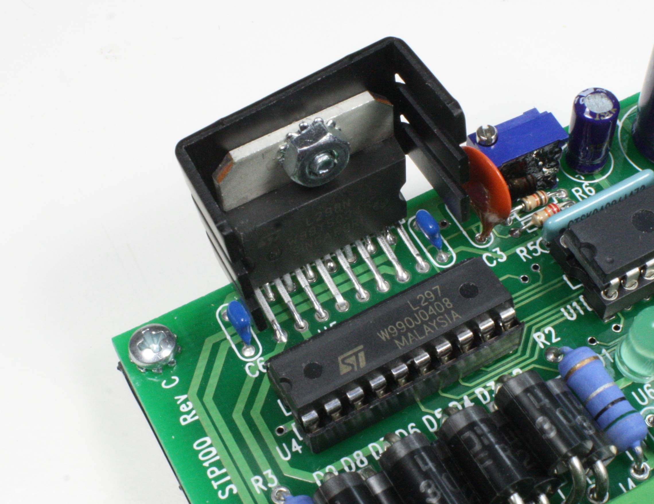
Figure 9-29. Heatsink on a motor controller PCB
Small transistor packages can also have thermal issues. Small press-on heatsinks composed of stamped metal fins are available for TO-5 and TO-18 packages. Figure 9-30 shows two examples of a TO-5 press-on heatsinks, along with a TO-5 part for comparison. A TO-18 heatsink is similar, just slightly smaller. Heatsinks for the TO-5 and TO-18 packages are also available as extruded aluminum parts, tubes with flared tabs at one or both ends, and stamped metal assemblies that somewhat resemble hats.
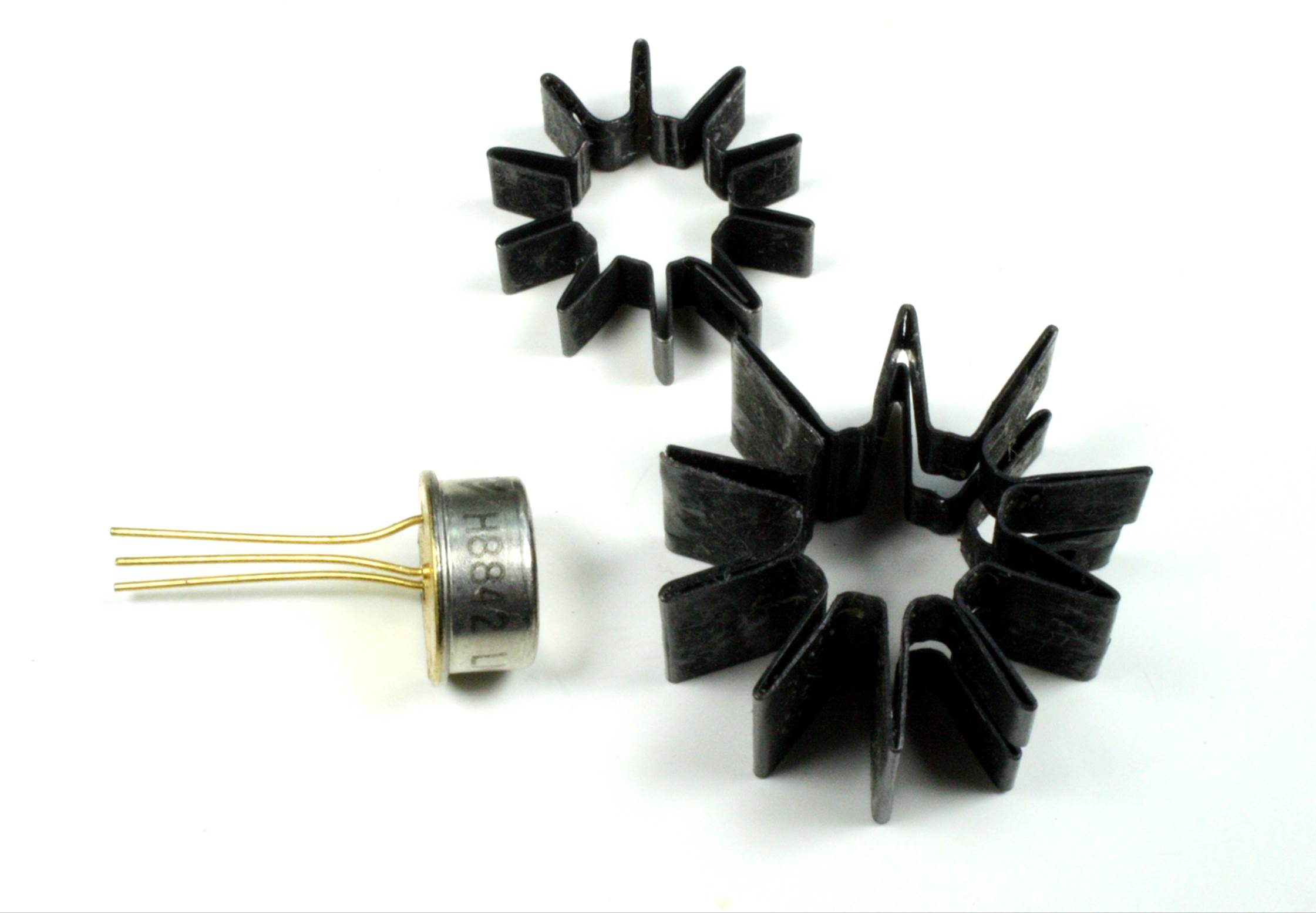
Figure 9-30. TO-5 press-on finned heatsink
Heatsinks are also available for TO-92 type parts, although in some situations you can mount the part against a metal panel or even a large heatsink for another part by using a small bracket. The downside to this approach is that the leads sometimes must be extended with wires (and the soldered connections covered with heat-shrink tubing) in order to reach the PCB.
A freestanding heatsink is a potential source of high voltage, such as in power supplies. Even in a low-voltage circuit, a heatsink might be at full V+ potential, and creating a short to ground can do some serious damage. Never touch a freestanding heatsink with your fingers or a grounded tool while the circuit is active.
Heavy-duty heatsinks are usually made from aluminum extrusions, which are then cut and drilled for a specific transistor package style. These are found in the output stages of high-power amplifiers, linear DC power supplies, and motor controllers, or anywhere else a lot of heat needs to be pulled away from a part and safely dissipated.
Note that, in order for a heatsink to be effective, it must itself have some way to dump the heat it has accumulated from a transistor or other part. You typically accomplish this by moving air over the heatsink with a fan of some type. In some instances, as on the heatsink of the CPU in a PC, the fan can be mounted directly onto the heatsink. In other designs, the heatsink fins protrude from the chassis of the device (or might be part of the chassis itself) and the flow of air in the local environment is sufficient. This type of arrangement is often seen with high-power audio amplifiers used in automobiles, VHF transceivers for mobile applications, and battery-powered AC inverters.
Integrated Circuits
A typical integrated circuit is a small square or rectangular piece of silicon crystal onto which active components and circuit traces are placed using photo-lithographic means. This piece of silicon is usually referred to a chip, although the entire integrated circuit (IC) is also called a chip. The surface features in modern ICs are extremely small, allowing extremely high circuit density. Modern microprocessor chips might contain millions of individual transistors.
The origin of the IC goes back over 60 years but didn’t become commercially viable until around 1958 when Jack Kilby of Texas Instruments patented the first practical IC using germanium as the base semiconductor material. This was followed shortly thereafter by Robert Noyce’s development of a silicon-based IC at Fairchild Semiconductor.
ICs can be broadly divided into two categories: linear and digital. The boundary between the two types is not always distinct, depending on what is in the circuitry of the IC. Linear devices are basically anything that isn’t digital, such as operational amplifiers (op amps). Linear devices are designed to work with a continuously variable signal, voltage, or current, and theoretically can have an infinite number of operating states. A digital device operates on discrete binary values at specific voltages to perform certain logic functions and can have only a limited number of operating states.
An op amp IC is the modern equivalent of a circuit that was originally developed for use in analog computers. The operating principle of an op amp is straightforward: it is designed to use feedback to force its input to zero volts by changing the value of the output. By carefully selecting the components that form the feedback circuit, a small input voltage can cause a large change in the output. Refer to Appendix A for a brief overview of op amp circuit theory.
A digital IC can be anything from a simple logic gate (AND, OR, NAND, NOR, etc.) to a microprocessor or microcontroller. Digital circuits operate on bits: discrete values of either 1 or 0, true or false. Chapter 11 discusses logic ICs and microprocessors, so the main focus here will be on the packages available.
Still other types of ICs can be a mix of linear and digital, such as analog-to-digital converters and direct digital synthesis (DDS) devices. IC packaging has also been used for things like resistor arrays, transistor arrays, and diode arrays.
Conventional IC Package Types
When integrated circuits were developed, one of the first challenges facing engineers was how to package them. Early packages came in styles that included flat, rectangular, ceramic bodies with leads protruding from two opposing sides. These were the original flat-pack styles. Later, the dual-inline package (DIP) styles were developed, again in ceramic. The plastic packages that are common today came later and have largely replaced the old ceramic types.
Figure 9-31 shows the basic dimensions of the two most common types of DIP packages. The size of a DIP package reflects, generally, the internal complexity of the IC inside of it and the number of external connections it provides. Small circuits such as a 555 timer or an op amp are usually packaged in an 8-pin style. Logic circuits such as the 74xx series devices typically come in 14- or 16-pin packages, with some larger devices using a 24- or 28-pin package. Memory devices are usually packaged in 24-, 28-, or 32-pin packages to provide for the memory addressing pins needed. Small (e.g., 8-bit) microprocessors usually have many interface pins for external memory and interface chips, so they are often packaged in a 40-pin DIP package. Larger microprocessors, such as some ARM-based parts, and the Intel and AMD CPUs (central processing units) found in PCs, can have over a hundred pins and come in pin-grid array (PGA), ball-grid array (BGA), and high-density surface-mount styles. Microcontrollers (microcontroller units, or MCUs), on the other hand, typically don’t have pins to access external memory, so the pin count can be very low even though the internal logic may be quite complex. For example, the ATtiny85 MCU from Atmel or the PICmicro from Microchip Technology are both available in 8-pin DIP packages.
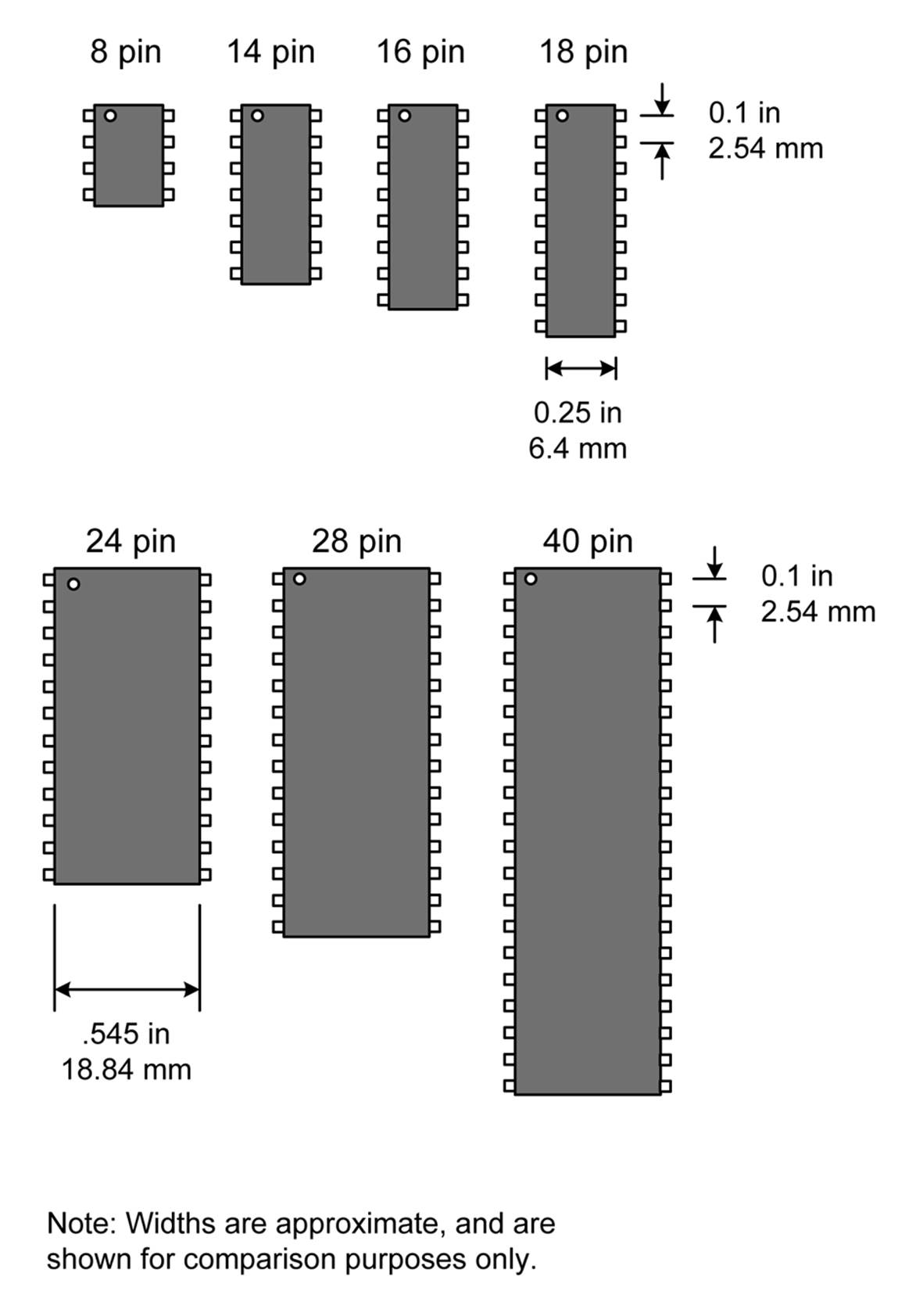
Figure 9-31. Through-hole DIP packages for integrated circuits
Figure 9-31 is intended to show the relative size differences between different types of DIP packages. It is not a precise reference. The width dimensions shown in Figure 9-31 are for the body width of the part, not the tip-to-tip width for the pins. There is some degree of variance possible in both the body width and the width-wise pin spacing, so the dimensions shown here must be considered to be approximate. The pin-to-pin spacing or pitch, at 0.1 inches or 2.54 mm, is a standard that just about every IC manufacturer follows. The definitive reference for DIP IC dimensions is the datasheet provided by the manufacturer. Fortunately, you can generally trust the layout templates in most PCB layout software packages to get DIP packages right, and a part that is slightly off-nominal will still fit on the PCB or a solderless breadboard. In fact, it is the PCB that defines the actual final pin-to-pin width dimension for a DIP IC, and the leads usually require some forming during assembly in order for the part to fit correctly into the pad holes on the board. There are special IC insertion tools made for just this purpose.
There are also 4-, 6-, and 64-pin DIP styles. The 4- and 6-pin styles are used for things like opto-isolators, but the 64-pin package is rare nowadays. Packages with high pin counts are typically fabricated in surface-mount styles.
Surface-Mount IC Package Types
Surface-mount packages for active devices come in a variety of sizes and styles. Some are large enough that they can be mounted on a PCB by hand with a good soldering station and some kind of magnification. Other types, such as BGA packages, with the connection points located under the body of the IC in a grid pattern, really cannot be hand-mounted and must be installed using specialized automated soldering equipment. Some packages are incredibly small, such as the C8051F30x series from Silicon Labs. These parts contain a complete 8051-type microcontroller in a surface-mount package measuring 3 mm × 3 mm.
Surface-mount IC packages vary in style, from some that aren’t much different from their DIP equivalents to those with leads so closely spaced that a workbench microscope is needed to work with them. Figure 9-32 shows some of the common surface-mount IC package types that are available.
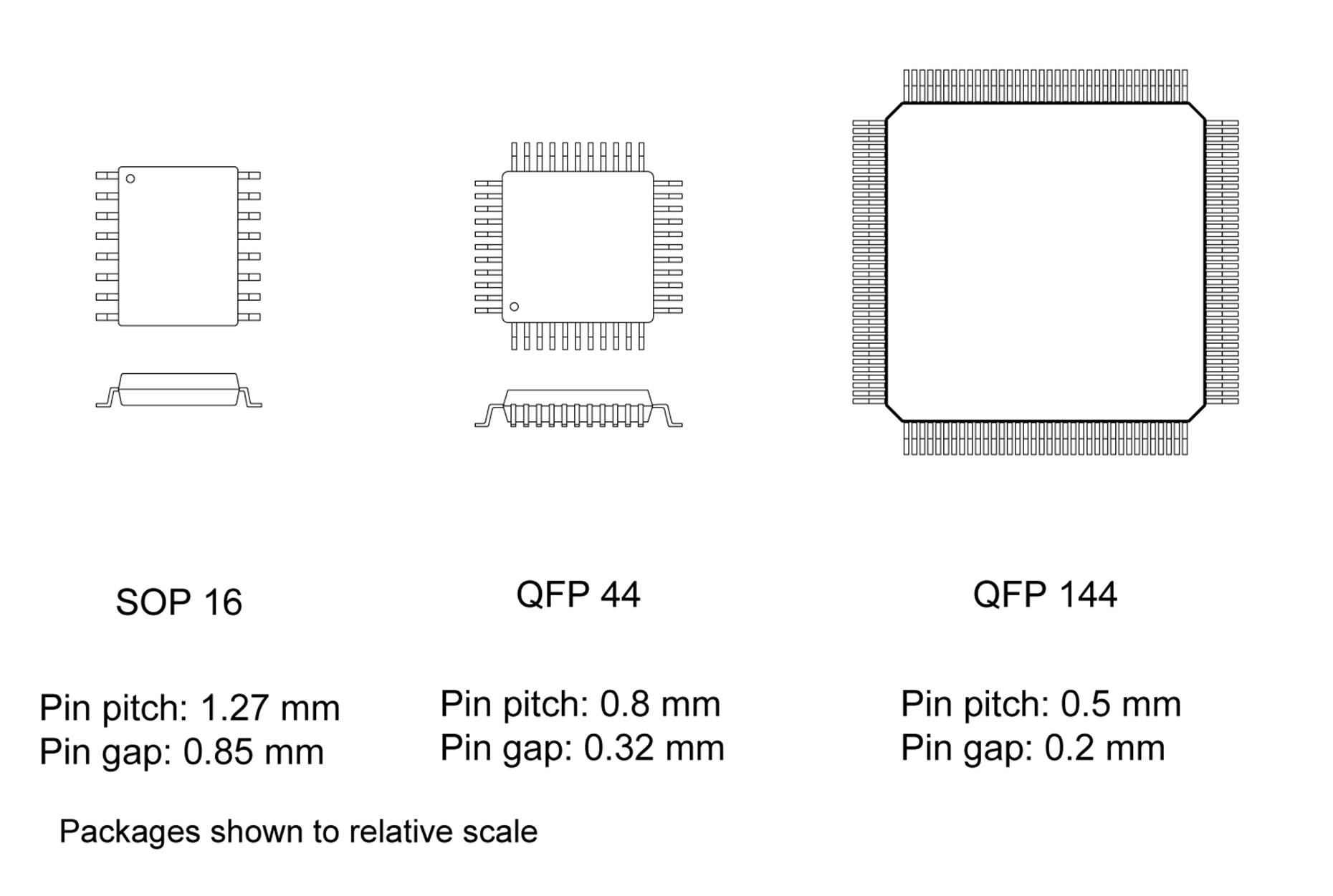
Figure 9-32. Examples of low-, medium-, and high-density SMT IC packages
The small-outline IC (SOIC) package family comprises a number of related packages. These range from the common SO, SOM, and SOL types to the high-density QSOP package. Table 9-5 lists some of the more commonly encountered members of the SOIC family (note that numbers in parenthesis are mm).
|
Name |
Description |
Body width |
Lead pitch |
|
SO |
Small Outline |
0.156 (3.97) |
0.050 (1.27) |
|
SOM |
Small Outline Medium |
0.22 (5.6) |
0.050 (1.27) |
|
SOP |
Small Outline Package |
0.3 (7.62) |
0.050 (1.27) |
|
SOL |
Small Outline Large |
0.3 (7.62) |
0.050 (1.27) |
|
VSOP |
Very Small Outline Package |
0.3 (7.62) |
0.025 (0.65) |
|
SSOP |
Shrink Small Outline Package |
0.208 (5.3) |
0.025 (0.65) |
|
QSOP |
Quarter Small Outline Package |
0.156 (3.97) |
0.025 (0.65) |
|
Table 9-5. SMD IC packages in the SOIC family |
|||
I should point out that this table is primarily for comparison purposes. The key features for each type are the body width and the lead pitch. The number of leads will depend on what is in the package, which can can range from 8 to 56. The types of leads (gull-wing, J-lead, flat) can vary from one manufacturer to another, even for packages with the same name, and the body dimensions can also vary slightly from what is listed here. As stated before, always check the datasheet for a part before committing it to a design.
Figure 9-33 shows the packages listed in Table 9-5 to scale.
High-Current and Voltage Regulation ICs
There are some types of parts that might look like a transistor, but are actually an IC. Voltage regulators are a perfect example of this. Other examples are various power op amps in TO-3 and large plastic packages that look like a wide TO-220 with many more pins. Power op amps are found in DC power control circuits, and some types are specifically designed for use in audio amplifiers. In fact, almost all home audio equipment made today uses these types of monolithic power amplifier modules.
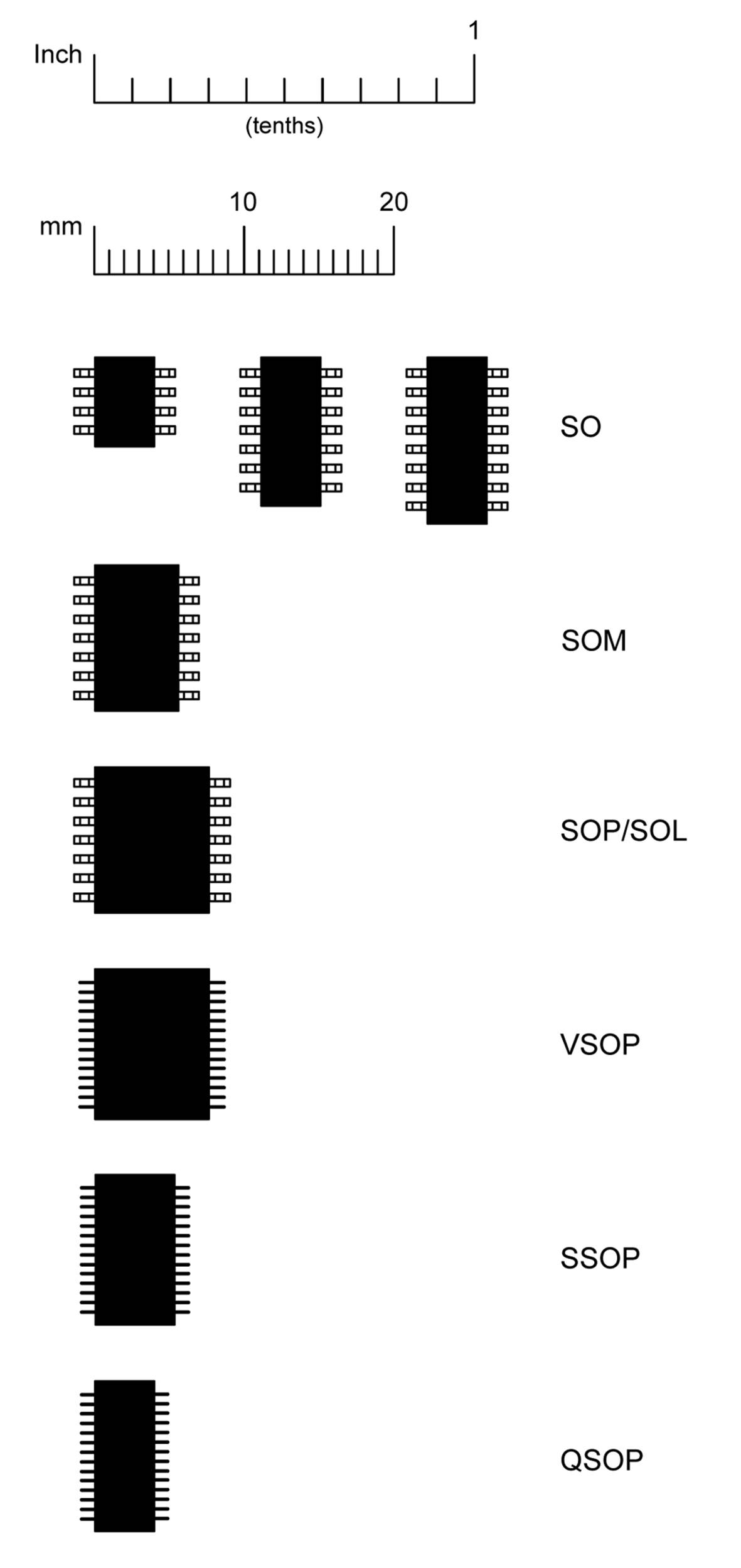
Figure 9-33. SOIC-type packages for integrated circuits
A linear voltage regulator IC is a handy thing when you need to produce a specific voltage level for a circuit, or some part of a circuit. These are basically a complete linear power supply in a TO-220 or SOT-223 package. The most basic types have terminals for input, output, and ground. Other types have the ability to adjust the output voltage via a control voltage (often set by a small potentiometer or a zener diode).
The 78XX and 79XX parts have been around for quite a while and are readily available. The “XX” is replaced with the output voltage of the device. The 78XX parts produce positive voltages, and the 79XX parts are used to produce negative voltages. These regulators are fixed output, with output voltages of 5, 8, 10, 12, 15, and 24 volts. Most are rated for around 1A of output current. I like to keep a small stock of 7805, 7905, 7812, 7912, and 7815 regulators on hand.
Low-current regulators are also available in TO-92 packages, such as the LM317. This is an adjustable device with an output voltage from 1.2 to 32V with 100 mA of output current. They are useful when working with analog-to-digital or digital-to-analog convertors that rely on a reference voltage (analog interfaces are discussed in Chapter 13).
Summary
The realm of active components encompasses a broad range of devices, all of which share the common feature of using an external source of current and having the ability to modify the way in which current moves through them in nonlinear ways. Some are externally controllable, whereas others rely on the intrinsic behavior of the solid-state material from which they are fabricated.
The basic P-N junction is the primary building block on which silicon-based solid-state discrete devices are built. If a device has just a single P-N junction, it is probably a diode or rectifier of some sort. Devices with multiple P-N junctions include BJTs, UJTs, FETs, SCRs, and TRIACs.
Integrated circuits incorporate multiple BJTs, FETs, and other components into a design that can be simple, such as an op amp or a 555 timer, to something as complex as the CPU in a computer with millions of individual components.
For experimenting and hacking, having a decent selection of discrete solid-state parts on hand is always a good thing. A bag of cheap 1N4148 diodes and some 1N4001, 1N4002, and 1N4003 parts come in handy when you are dealing with power supply circuits. LEDs can be purchased in the form of kits from a number of suppliers. Although these are basically just a box or a large bag containing smaller bags of parts, you can always sort them out and store them neatly yourself.
A basic selection of transistors (such as the ones listed in Table 9-3) can be used for anything under about 300 MHz. Unless you plan to work with RF, you generally won’t need anything faster. If you would like a large selection to work with, inexpensive kits of transistors are available, with a good selection of various types in neatly labeled little plastic bags.
When it comes to working with surface-mount parts, you will of course need the correct tools (such as the soldering equipment shown in Chapter 3) and to be able to use the soldering techniques illustrated in Chapter 4. SMT can be extremely challenging, so unless there is a definite need for it, I would suggest avoiding it, at least initially. A prototype is expected to look clunky, and if you are hacking something for fun, there’s really no need to try to make it production-ready. It doesn’t really matter, for example, if a hacked RoboSapien robot toy looks like it’s wearing a Buck Rogers backpack, so long as it works.
When you are working with solid-state components, static charge is your enemy, and it never sleeps. You should seriously consider purchasing an ESD wrist strap, at the very least. Anti-static mats aren’t very expensive, and putting one on your workbench (or on the kitchen table) will make your ESD prevention measures even more effective. It is extremely annoying to have just one part of a particular type left, only to discover that when you picked it up from its storage container some stray static charge got to it. It’s even worse to build something, test it, and then have it fail in use a week or a month later because one of the parts was partially damaged by ESD during construction.
Lastly, I can’t stress enough how important it is to get and read the datasheet for a part. I have seen parts in TO-92 packages that look like transistors but are really something else entirely or, worse yet, might have a common part number but have a pin-out that is uncommon. ICs can also be a problem in terms of packaging. Although the 7400 and 4000 series logic parts (discussed in Chapter 11) are generally consistent, microcontrollers, microprocessors, and other complex logic parts can have completely arbitrary pin-out configurations. Without a datasheet to guide you, it is nearly impossible to work with these components.
1 Dimensions are in millimeters; maximum values shown.
All materials on the site are licensed Creative Commons Attribution-Sharealike 3.0 Unported CC BY-SA 3.0 & GNU Free Documentation License (GFDL)
If you are the copyright holder of any material contained on our site and intend to remove it, please contact our site administrator for approval.
© 2016-2026 All site design rights belong to S.Y.A.