Practical Electronics: Components and Techniques (2015)
Chapter 14. Data Communication Interfaces
Call it the Internet of Things, or distributed systems, or whatever the term of the day happens to be, but it is a fact that for a gadget to be as useful as it possibly can be, it needs to be able to exchange data with other things. After all, a gadget sitting all by itself in the corner with nothing to talk to is a lonely gadget.
In the past, communication of data between various devices and systems was accomplished through slow RS-232 or 20 mA current loop serial links, or bulky portable media such as magnetic tapes, removable disk packs, and floppy disks. Early in the history of computing, punched paper cards and rolls of punched paper tape were initially used for this purpose.
Nowadays, we have USB flash drives, SD memory cards, portable hard drives, and Bluetooth, USB, WiFi, and Ethernet communications. But the end result is the same: data from one device or system is passed to another for processing, storage, or display (or all three), just a lot faster today than 10, 20, or 40 years ago. Sharing data in real time is now a commonplace feature of things like networked refrigerators, coffee pots, thermostats, and home entertainment systems. There has been talk of allowing automobiles to communicate with one another on the road to help avoid accidents, or between cars and roadside wireless communications points to dispense traffic advisories and warnings in a way that doesn’t require the driver to continuously listen to the radio or become visually distracted trying to read a flashing warning sign as it zips past.
In this chapter, we’ll look at the SPI and I2C methods used for chip-to-chip communications. SPI and I2C are not the oldest forms of data communication, but gaining an understanding of these two techniques (synchronous and asynchronous) will help set the stage for what follows. Next, we’ll cover the venerable RS-232 and RS-485 interfaces, the old-timers that are still going strong today. Then we’ll look at USB, the ubiquitous interface, with some examples of the component hardware available to work with it. Ethernet comes next, in both wired and wireless forms. Lastly, we’ll wrap up with a look at newer wireless technologies such as Bluetooth, ZigBee, and short-range VHF links.
As we go along, you might start to see some similarities between the various communications techniques. Some are synchronous (which requires a clock signal), and some are asynchronous (the timing is implicit in the stream of bits). Some use differential signaling (a +/– pair of wires), and some don’t. Some use wires, and others operate at radio frequencies. But the one primary characteristic shared by all of the protocols we’ll cover is that they are serial interface techniques.
We won’t cover things like the parallel port on a PC (which has some interesting possibilities if you are willing to tilt your head to the side and look at it as something other than a way to control a printer), nor will we poke into the mysteries of the GPIB interface used in instrumentation applications. If you’re curious, you can find out more about these topics from the books referenced in Appendix C.
If there are any technical terms or concepts presented here that might not be immediately clear, I’ll make a point to give a reference to other places in the book that might help shed light on them, but in any case, don’t forget about basic electronics theory in Appendix A, the Glossary, and the bibliography in Appendix C. Lastly, there are a lot of component parts listed in this chapter. If you want definitive information about them, be sure to visit the manufacturer or vendor’s website (either given here or in Appendix D) and download the datasheets and reference documents.
Also, you might notice that many of the images of PCB modules shown in this chapter are Arduino shields. It’s not that I’m particularly partial to all things Ardunio (although I am rather fond of it); it’s just that the advent of the Arduino has spurred something of a minor renaissance in hobbyist and experimenter electronics and microcontrollers. The result has been a flood of inexpensive Arduino clones, derivatives, and add-on modules using parts that would have otherwise gone buried in a consumer electronics device. If nothing else, these modules show just how easy it can be to use the parts listed in this chapter in your own creations.
Although this chapter refers to specific part numbers and manufacturers by name, this does not in any way constitute an endorsement. I provide this information for your benefit by showing some examples of what is available at the time of this writing. For the latest information, and a broader view of what is available, see Appendix D. Appendix E lists all of the component parts mentioned in this book.
Basic Digital Communications Concepts
The primary concept behind all digital communications methods is that they pass data as binary values, either serially (one bit after another) or in parallel (with whole groups of bits moving in unison). Although the technology may have evolved over time, these basic concepts apply to any form of digital communications.
A digital data stream can be sent over a wire or passed around in the form of radio waves. The radio signal gets converted back into a digital stream at the receiving end. Data that moves in parallel needs some way for the sender and receiver to coordinate who is talking and who is listening. And parallel data can be converted into a serial form and then reconstructed as parallel data at the other end. In the following sections, we’ll cover the high points of these and other topics before moving on to examine particular examples.
Serial and Parallel
Digital data communication interfaces can be divided into two broad catagories: serial and parallel. Serial data is where a digital value—a byte (8 bits), for example—is sent over a single channel (e.g., a wire) one bit at a time. At the receiving end, each bit is read and then reassembled once again as a byte. Figure 14-1 shows the process of serializing and reconstructing digital data.
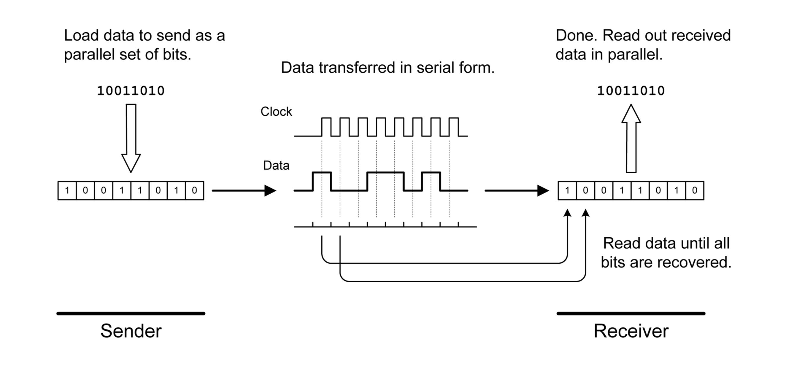
Figure 14-1. Serial data exchange
Figure 14-1 shows what is known as a synchronous serial interface, meaning that the sending and receiving of data bits is coordinated by a clock signal sent from the sender to the receiver. The vertical dashed lines indicate when the receiver will look at the incoming signal to detect if it is either high (1) or low (0). This can occur at the start (rising edge) or end (falling edge) of each clock pulse. In this case, it’s shown on the rising edge of the clock pulses. In the next section, we’ll look at an asynchronous way to do this, which doesn’t require a clock.
With a parallel data interface, an entire byte (or word, or even something larger) is transferred all at once from sender to receiver. As you might surmise, a parallel interface can be much faster than a serial type, since the parallel-to-serial (and back again) steps are eliminated. The downside is that a parallel interface needs a sufficient number of wires to carry all the individual bits. Figure 14-2 shows an example of a parallel interface.
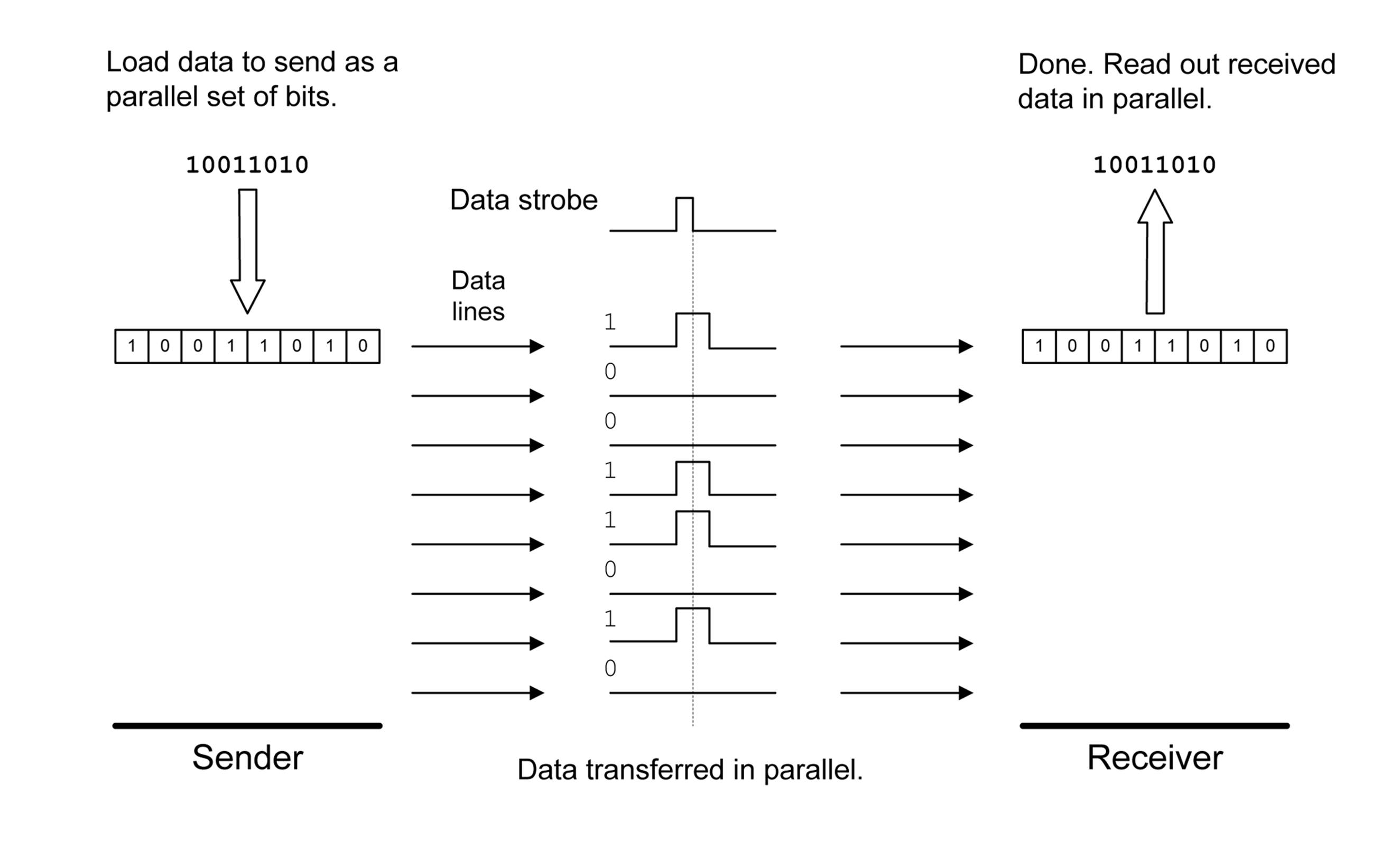
Figure 14-2. Parallel data exchange
For a parallel data transfer, only one control pulse (labeled “Data Strobe” in Figure 14-2) is absolutely necessary. When the receiver detects this pulse it will read in (or latch, in digital terminology) the data on the parallel lines into a data register. As with Figure 14-1, the dashed vertical represents the time when the data is actually sensed and loaded into the receiver’s register.
High-speed parallel data interfaces have been used as interconnection channels between the processing modules of supercomputers, where the need for speed trumps the cost of the wiring and circuit complexity. The more pedestrian PC parallel interface used for things like printers and plotters operates on the same principles, just much more slowly. If you would like to find out more about parallel interfaces and some of the interesting ways the printer port on a PC can be hacked, take a look at some of the titles listed in Appendix C.
Synchronous and Asynchronous
The terms synchronous and asynchronous refer to the way in which a data transfer is handled between sender and receiver. A synchronous interface relies on the use of a clock signal or transfer pulse for coordinating the data transfer timing, whereas an asynchronous interface does not. Figures 14-1 and 14-2 are examples of synchronous interfaces. Almost all parallel interfaces are synchronous, whereas serial interfaces aren’t always synchronous but can instead be asynchronous.
An asynchronous data interface is almost always a serial interface. The asynchronous part comes from how a receiver for this type of interface detects incoming data and automatically synchronizes itself to the incoming stream of bits from the sender. Once the start of the incoming data stream is detected, the receiver will look for a specific number of bits, with each group of bits forming a byte (or character, in some cases) of data. Figure 14-3 shows a block diagram of an asynchronous serial interface that employs two UART (universal asynchronous teceiver-transmitter) devices to handle the parallel-to-serial conversion and then back to parallel again.
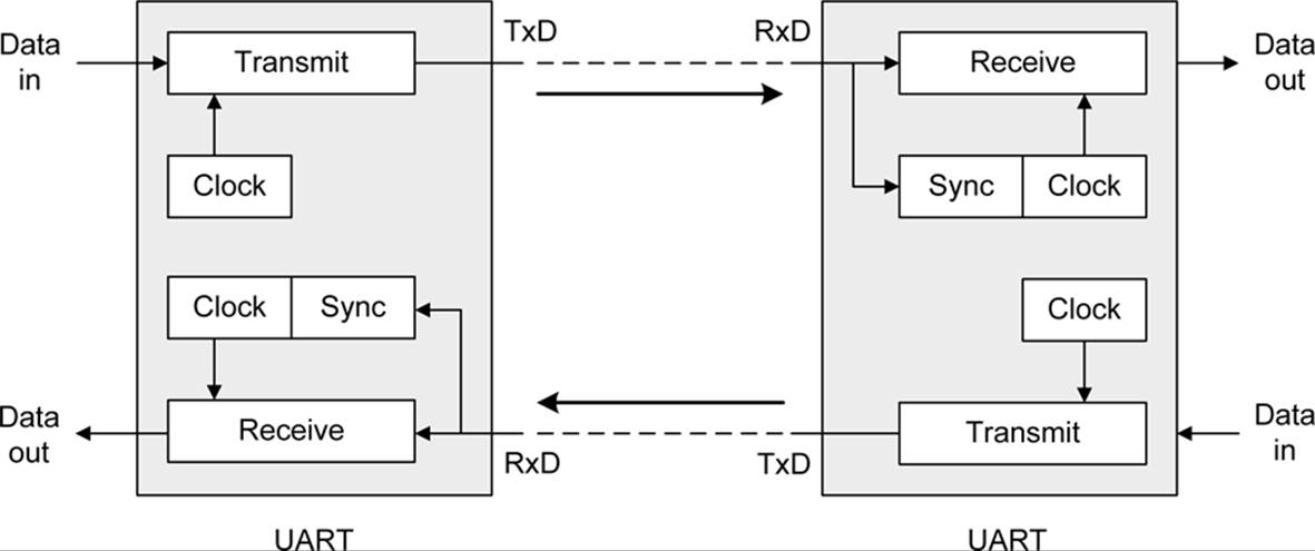
Figure 14-3. UART device block diagram
In Figure 14-3, you can see that the transmit part of a UART uses a definite clock rate to control how fast the data is pushed out to the receiver. The receiver, on the other hand, relies on a sync circuit to detect the incoming data from the transmitter and adjust an internal receive clock to match the data rate.
Most modern microcontrollers incorporate one or more UART functions into their design. If you want to use these functons for RS-232 or RS-485 interfaces, all you need to do is add some components to convert the signals to the appropriate voltage levels for the particular protocol. I use the term function here, because in modern microcontrollers, the UART is just part of the silicon chip, not a separate outboard component as in the past. There are standalone UART devices available, and “RS-232” takes a closer look at how the data used with RS-232 is formatted and the data transfer speeds available. “RS-485” covers the RS-485 interface.
HALF- AND FULL-DUPLEX
The terms half-duplex and full-duplex refer to the data transfer modes used with a pair of devices communicating over a channel of some sort. In a half-duplex system, each end of the connection has both a transmitter and a receiver, but they are never active simultaneously. Data moves in only one direction through the channel at any given time. USB and I2C interfaces are half-duplex, and RS-485 is typically implemented as a half-duplex interface. A full-duplex system has two separate channels with a transmitter at one end and a receiver at the other, and the channels move data in opposite directions simultaneously. The transmitter on a channel can send whenever there is data ready to transmit. SPI, RS-232, and Ethernet are examples of full-duplex digital data communication interfaces.
SPI and I2C
This section covers the basics of the SPI and I2C short-range, chip-to-chip communications protocols. These are serial communications protocols that are easy to implement and easy to use. They also help to keep chip pin counts low by requiring only 2, 3, or 4 signals to implement, as opposed to 10 or more for a parallel interface. But convenience comes at a price (as always): for a given clock speed, a serial interface is not as fast in terms of bandwidth (the data equivalent of current, or amount of bits moved per second) as a parallel interface. Still, for many applications, the compactness and convenience outweigh the limited bandwidth.
Although other variations on short-range serial interfaces have been devised over the years, the two that still stand out and have passed the test of time are SPI and I2C, so these are the ones we will focus on here. Other interfaces, such as the Dallas/Maxim one-wire interface, have their place, and you can read up on this method, and others, in the application notes and manual available on the chip manufacturer’s websites (see Appendix C).
SPI
The abbreviation SPI stands for serial peripheral interface. It is a full-duplex, four-wire synchronous serial interface designed for chip-to-chip communications, first defined by Motorola (now Freescale) around 1979. It has since become a de facto industry standard. You can find SPI interfaces on microconrollers, I/O expansion ICs, SD memory cards, and sensor devices, just to name a few things. SPI is capable of very fast data transfers, with the only real limitations being the hardware’s ability to generate and detect the clock signal reliably and move data without errors.
Interestingly, it wasn’t until relatively recently that anything like a standalone specification document was available for SPI. Prior to about 2000, information about the SPI protocol had to be gleaned from various microprocessor and microcontroller datasheets and user manuals. In 2000, Motorola released a semiformal SPI specification, the “SPI Block Guide.”
SPI devices communicate in a master/slave arrangement, where the master device always initiates the data exchange, rather like USB (the terms master and slave are historical at this point and refer to the control-response protocol implemented by SPI). SPI uses four signal lines: SCLK, MOSI, MISO, and SS, as defined in Table 14-1.
|
Signal |
Definition |
Direction |
|
SCLK |
Serial clock |
Master to slave |
|
MOSI |
Master out, slave in |
Master to slave |
|
MISO |
Master in, slave out |
Slave to master |
|
SS |
Slave select (active low) |
Master to slave |
|
Table 14-1. SPI signal lines |
||
In SPI terminology, a master device, typically a microcontroller or microprocessor, is connected to an SPI slave device. For every bit sent by the master on the MOSI line, the slave will return a bit at the same time on its MISO line. The result is that during each clock cycle (the SCLK line), a full-duplex data transfer occurs. Because SPI does not use device addressing, you must specifically select each slave device using the SS line. Figure 14-4 shows two different ways to arrange this.
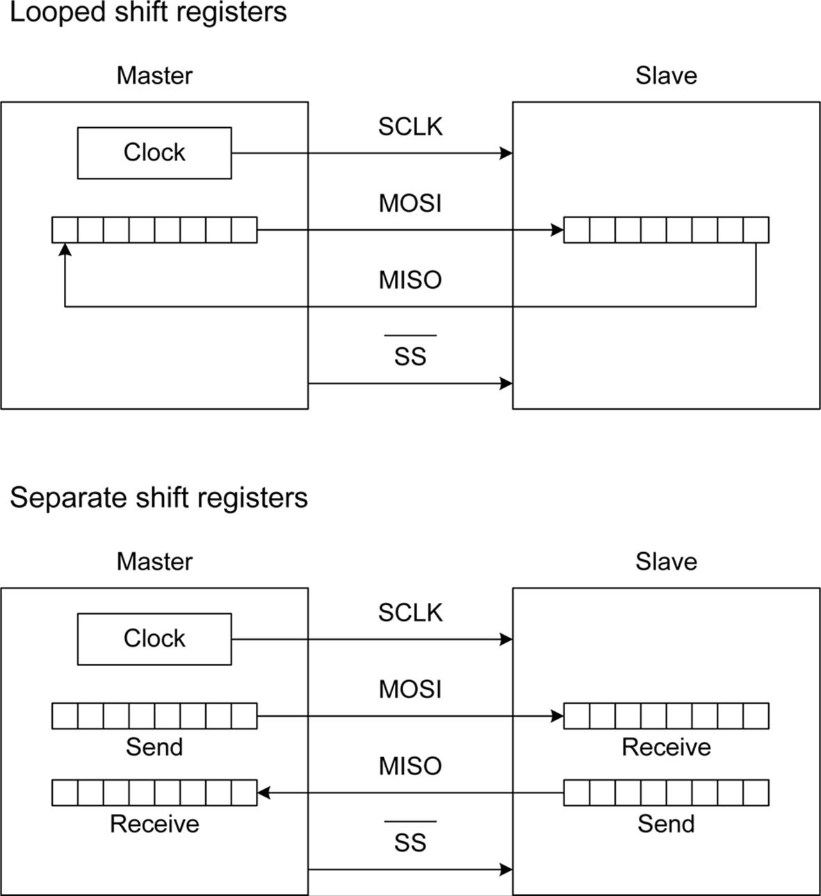
Figure 14-4. Master and slave shift-register operations for full-duplex communications.
Each slave device waits for a control input (the SS line) to go low. When this occurs, it will start to “clock in” data from the master device synchronously with the SCLK signals. Figure 14-5 shows a simplified timing diagram for SPI data transfers.
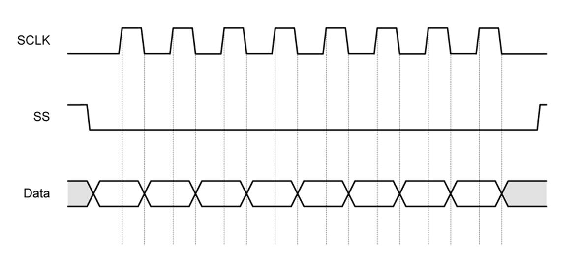
Figure 14-5. SPI data transfer timing diagram
In Figure 14-5, the data is changed (or toggled) on the falling edge of a clock pulse and read on the rising edge. Each of the odd-looking boxes on the data line represents a single bit of data, which can be either low (0) or high (1). When the SS line is high (inactive), a slave will cause its MISO pin to go into what is called a high-Z (or high impedence) state. This effectively removes it from the circuit until the SS line to that particular slave device is once again pulled low.
Figure 14-5 shows only one possible configuration for an SPI interface. The are four different modes that define the clock polarity and how the clock pulses will be toggled and sensed. Refer to the “SPI Block Guide” for details about the clock polarity options. Note that the master and its slave devices must use the same clock and data modes in order to communicate, and most slave devices are hardwired when they are fabricated for one of the four possible modes. If a master is connected to multiple slaves with different clock modes, it will need to reconfigure itself for each slave as necessary.
You can connect multiple SPI devices to a single master by providing each one with its own SS line, as shown in Figure 14-6. There is no real limit to how many slaves a master can control; it’s just a matter of having enough SS lines available. These are usually taken from the general-purpose DIO (digital or discrete I/O) lines of a microcontroller.
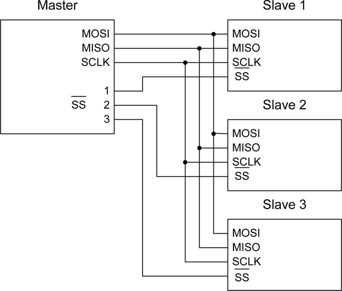
Figure 14-6. Multiple SPI slave devices with a single master
By now, you might be wondering how an SPI slave could have something to send back to a master if it is in the middle of receiving a command or data. The answer is that, unless the master is expecting something from the slave, it simply ignores whatever is sent back. This also applies to the slave when it is sending back a response to a command it received in a previous operation. It will ignore whatever the master sends and send back the response it has already prepared. Figure 14-7 shows how this works for a Maxim MAX7317 10-port I/O expander IC as a two-step process.
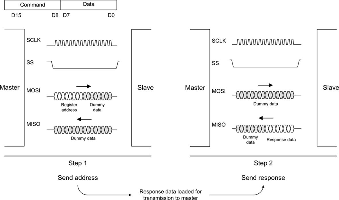
Figure 14-7. Example command and response sequence for a MAX7317 I/O expander IC
To read the state of one of the input ports on the MAX7317, the master first sends 16 bits off to the slave. The bits from D8 to D15 are an 8-bit command and address value. Bits D0 to D7 are data. When you are reading a port, only the command and address bits matter; the data bits are ignored (they are labeled as “Dummy data” in Figure 14-7). The master then raises the SS (or CS, chip select, as Maxim calls it) briefly and then sends 16 bits of dummy data while the 7317 returns 8 bits of dummy command and address data along with 8 bits of data containing the state of the port specified in the preceding command.
There is no limit on how many bits can be used to communicate with a slave device. Some devices use 8 bits, others use 16, and some might use more (such as SD flash memory cards). SCLK can be stopped and restarted in the middle of a transmission, if necessary. So long as SS is low, the interface is considered to be active (this is one of the advantages of a synchronous interface, by the way). Internal operations in a slave device typically occur when SS goes high (signalling the end of the transaction) and the slave device is deselected.
I2C
Like SPI, I2C (also written as I2C and pronounced “Eye-squared-cee”) was designed to provide a short-range interface for connecting ICs, sensors, and other components at the circuit board level. It is not intended to be used to connect things to a PC, although it is possible to do that with the correct interface components. Some kits, such as the Velleman K8000 interface board, use this technique. Unlike SPI, the I2C interface is multi-master and uses an addressing scheme rather than chip select (SS) lines. Figure 14-8 shows multiple I2C devices connected in parallel.
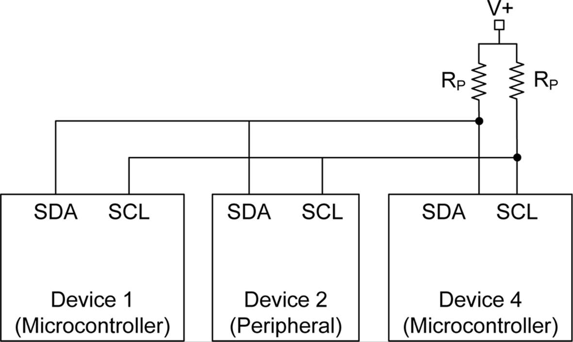
Figure 14-8. Multiple connected I2C devices
Whereas SPI did not start out with an official specification, I2C was formally documented by Philips Semiconductors (now NXP) from the outset. The official I2C specification and user guide is available on NXP’s website.
I2C uses only two bidirectional signal lines: the Serial Data Line (SDA) and the Serial Clock Line (SCL). There is no select line, and because it’s a half-duplex interface, it requires only a single data line. These are open-drain lines, meaning that the drain of an internal FET is brought out to the SDA and SCL pins. It also means that external pull-up resistors are mandatory for an I2C interface. The pull-up voltage is typically from 3.3V to 5V, depending on the component’s I2C interface specifications. A communication transaction on an I2C bus occurs when one of the devices, acting as the current master, places the two bus signals into a START condition. This serves as signal to other I2C devices that a master wants to communicate. When a start condition occurs, all other I2C devices will “listen” to the bus for incoming data.
After the START condition, the master sends the address of an I2C device. It also sends an indication of the type of action to be performed, either read or write. Once the rest of the I2C devices receive the address, they will compare it to their own. If there is no match, they simply wait in the listening state until the bus is released by a STOP condition. Otherwise, if the address matches one of the I2C devices on the bus, it will generate an acknowledge response to the master.
Upon receipt of the acknowledgment, the master will either start transmitting data or it will listen for the addressed slave to return data to it. This depends on whether the address was a write address or a read address. When reading data, the master responds to each byte from the slave with an acknowledgment. When the data transmission is complete, the master releases the I2C bus by setting it into the STOP condition.
I2C is relatively easy to work with, but that high-level simplicity hides the low-level complexity. For example, using I2C with an AVR microcontroller involves writing data to internal registers that control the two-wire interface (TWI) subsystem in the microcontroller. The TWI contains the logic necessary to set the START and STOP states, control the transmission speed (the bit rate), and perform address matching. It also handles the acknowledgments and checks for possible bus collisions (arbitration) if another device should happen to already be the master on the bus.
The steps necessary for an AVR microcontroller to carry out a complete I2C data transaction are the same as those outlined earlier. However, each brand of microcontroller with I2C support might do things in a slightly different way using slightly different logic, but the basic order of operations is defined as part of the I2C standard.
I2C supports either 7- or 10-bit addresses, depending on the devices used. In the original 7-bit design, shown in Figure 14-9, the least significant bit (LSB) indicates if the address will be used to read or write from the master device. The remaining 7 bits constitute the actual address of a specific I2C peripheral device on the bus.
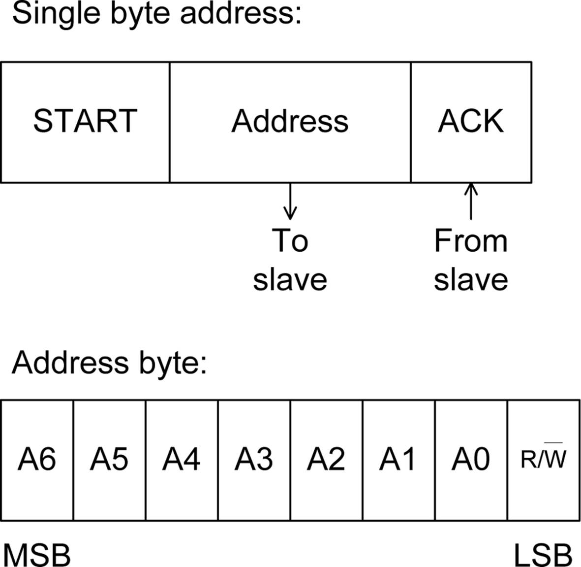
Figure 14-9. 7-bit I2C address format
A 10-bit address consist of 2 bytes, and the address is sent in two steps, as shown in Figure 14-10. The most significant byte is sent first, then the least significant byte. Notice that, when the 10-bit form is used, the slave sends an acknowledge (ACK) for each of the 2 address bytes.
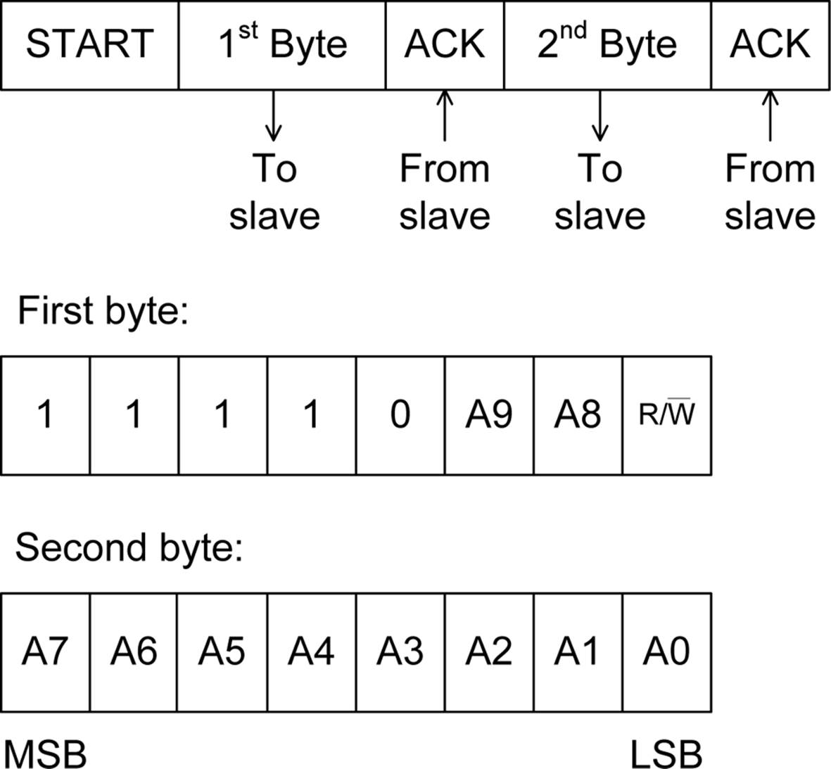
Figure 14-10. 10-bit I2C address format
An address is usually assigned to a part when it is created and put into production. For high-volume components, the usual method is to request an address assignment from NXP (formerly Philips). If you are connecting two microcontrollers, you might be able to assign any address you wish, but choose wisely.
Some address values, listed in Table 14-2, have been designated as reserved by NXP.
|
Address byte |
R/W bit |
Description |
|
0000 0000 |
0 (write) |
General call address |
|
0000 0001 |
1 (read) |
START byte |
|
0000 001X |
Don’t care |
CBUS address |
|
0000 010X |
Don’t care |
Reserved |
|
0000 011X |
Don’t care |
Reserved |
|
0000 1XXX |
Don’t care |
Hs-mode master code |
|
1111 1XX1 |
1 (read) |
Device ID |
|
1111 0XXX |
Don’t care |
10-bit slave addressing |
|
Table 14-2. I2C reserved 7-bit addresses |
||
Note that the address byte column in Table 14-2 shows the 8 bits in the address byte, and recall from Figure 14-9 that the least significant bit of the address is the read/write control bit. Also, when a bit position is marked as “don’t care,” it means that the bit value (whatever it may be) will be ignored by the I2C devices involved. For more detailed information about these reserved addresses, refer to the NXP I2C specification document. In most cases, the 10-bit address will be used the most.
There is no official list of I2C address assignments. NXP’s position on this is that if it published all the known address assignments, people might decide to claim an unused address for a new product without going through NXP. This could, of course, lead to conflicts between an “official” address and a “rogue” address. Limor Fried (the founder of Adafruit) and her associates have started to collect and post the I2C addresses they run across.
The I2C specification defines four distinct speeds (or bit rates) for I2C interfaces, listed in Table 14-3.
|
Designation |
Name |
Max rate (Kbits) |
|
Sm |
Standard-mode |
100 |
|
Fm |
Fast-mode |
400 |
|
Fm+ |
Fast-mode Plus |
1,000 |
|
Hs |
High-speed mode |
3,400 |
|
Table 14-3. I2C bit rates |
||
There is also an “Ultra Fast-mode” available for use with a unidirectional bus that supports a maximum rate of 5 Mbits/s, but it is not compatible with conventional I2C interfaces.
A Brief Survey of SPI and I2C Peripheral Devices
Memory, discrete I/O ports, multi-axis accelerometers, color LCD displays, wireless communication modules, and many more things are all available with either SPI or I2C interfaces, or, in some cases, both. These two serial interface protocols are a major part of modern electronics, and many of the clever gadgets we take for granted today would be impossible without them.
This section is intended to give a glimpse of what is available, and provide some jumping-off points for your own investigations. The parts listed have been selected on the basis of functionality and availability, but this section lists only a small fraction of what is available. To see what else is available, check out the major electronics distributors listed in Appendix D. Be prepared to spend a few hours (or more) looking through the available parts.
Discrete I/O
If you need to output a set of parallel or discrete bits, but you are running out of digital I/O lines, using a serial-to-parallel device is one way to get there from here. Table 14-4 lists a few of these types of devices that use either I2C or SPI serial interfaces and provide from 8 to 16 discrete digital I/O ports.
|
Part number |
Manufacturer |
Ports |
Interface |
|
PCF8574 |
Texas Instruments |
8 |
I2C |
|
MAX7317 |
Maxim |
10 |
SPI |
|
MCP23017 |
Microchip |
16 |
I2C |
|
Table 14-4. I2C and SPI discrete I/O port expansion chips |
|||
Say, for example, you want to control a set of LEDs on a front panel using just two pins on the microcontroller. The PCF8574 from Texas Instruments provides 8 discrete I/O ports with an I2C serial interface. The Microchip MCP23017 is a device with 16 discrete ports that also uses an I2C interface. If SPI is preferred over I2C, the Maxim MAX7317 is one example of an I/O expander that provides 10 discrete I/O ports with an SPI interface.
ADC and DAC Devices
A multitude of ADC and DAC devices are available with either SPI or I2C interfaces, in a wide range of resolutions, conversion speeds, and number of channels. For a listing of ADC and DAC devices with serial interfaces, see Chapter 13.
Memory
Memory devices are probably the most common SPI and I2C peripherals. Available types include EEPROM (electrically erasable programmable read-only memory), serial SRAM (static RAM), and, of course, flash. The ubiquitous SD flash memory cards (and their smaller cousins, the microSD cards) use an SPI interface, and EEPROM memory is available with both SPI and I2C interfaces, as shown in Table 14-5. See Tables 14-6 and 14-7 for available serial SRAM devices and flash devices, respectively.
|
Part number |
Manufacturer |
Size (bits) |
Organization |
Interface |
|
AT25010B |
ATMEL |
1Kb |
128 × 8 |
SPI |
|
AT24C01D |
ATMEL |
1Kb |
128 × 8 |
I2C |
|
AT25020B |
ATMEL |
2Kb |
256 × 8 |
SPI |
|
AT24C02D |
ATMEL |
2Kb |
256 × 8 |
I2C |
|
PCF85103C-2 |
NXP |
2Kb |
256 × 8 |
I2C |
|
PCF8582C-2 |
NXP |
2Kb |
256 × 8 |
I2C |
|
AT25040B |
ATMEL |
4Kb |
512 × 8 |
SPI |
|
AT24C04C |
ATMEL |
4Kb |
512 × 8 |
I2C |
|
PCF8594C-2 |
NXP |
4Kb |
512 × 8 |
I2C |
|
AT25080B |
ATMEL |
8Kb |
1,024 × 8 |
SPI |
|
AT24C08D |
ATMEL |
8Kb |
1,024 × 8 |
I2C |
|
PCA24S08A |
NXP |
8Kb |
1,024 × 8 |
I2C |
|
PCF8598C-2 |
NXP |
8Kb |
1,024 × 8 |
I2C |
|
AT25160B |
ATMEL |
16Kb |
2,048 × 8 |
SPI |
|
AT24C16D |
ATMEL |
16Kb |
2,048 × 8 |
I2C |
|
AT25320B |
ATMEL |
32Kb |
4,096 × 8 |
SPI |
|
AT24C32D |
ATMEL |
32Kb |
4,096 × 8 |
I2C |
|
AT25640B |
ATMEL |
64Kb |
8,192 × 8 |
SPI |
|
AT24C64B |
ATMEL |
64Kb |
8,192 × 8 |
I2C |
|
AT25128B |
ATMEL |
128Kb |
16K × 8 |
SPI |
|
AT24C128C |
ATMEL |
128Kb |
16K × 8 |
I2C |
|
AT25256B |
ATMEL |
256Kb |
32K × 8 |
SPI |
|
AT24C256C |
ATMEL |
256Kb |
32K × 8 |
I2C |
|
AT25512 |
ATMEL |
512Kb |
64K × 8 |
SPI |
|
AT24C512C |
ATMEL |
512Kb |
64K × 8 |
I2C |
|
AT25M01 |
ATMEL |
1Mb |
128K × 8 |
SPI |
|
AT24CM01 |
ATMEL |
1Mb |
125K × 8 |
I2C |
|
Table 14-5. EEPROM memory |
||||
|
Part number |
Manufacturer |
Size (bits) |
Organization |
Interface |
|
23A512 |
Microchip |
512 Kb |
64K × 8 |
SPI |
|
23A1024 |
Microchip |
1 Mb |
128K × 8 |
SPI |
|
N01S830HAT22I |
ON Semiconductor |
1 Mb |
128K × 8 |
SPI |
|
FM25H20 |
Cypress |
2 Mb |
256K × 8 |
SPI |
|
PCF8570 |
NXP |
2 Mb |
256K × 8 |
I2C |
|
Table 14-6. Serial SRAM memory |
||||
|
Part number |
Manufacturer |
Bits |
Channels |
Interface |
|
M25P10 |
Micron |
1 Mb |
125K × 8 |
SPI |
|
SST25VF010A |
Microchip |
1 Mb |
128K × 8 |
SPI |
|
SST25VF020B |
Microchip |
2 Mb |
256K × 8 |
SPI |
|
SST25VF040B |
Microchip |
4 Mb |
512K × 8 |
SPI |
|
SST25VF080B |
Microchip |
8 Mb |
1Mb × 8 |
SPI |
|
SST25VF016B |
Microchip |
16 Mb |
2Mb × 8 |
SPI |
|
M25P16 |
Micron |
16 Mb |
2Mb × 8 |
SPI |
|
N25Q00AA11G |
Micron |
1 Gb |
128Mb × 8 |
SPI |
|
Table 14-7. Flash memory |
||||
Displays
LCD display controller chips, such as the ILI9325C from ILI Technology Corporation, provide the control functions necessary to operate a touchscreen color LCD display with 256 × 320 display resolution. Modules based on this chip typically use an SPI interface, and the data rate is high enough to display near real-time video.
Standard two- and four-line LCD displays, like the one shown in Figure 14-11, are available with I2C and SPI interfaces. These are good for things that don’t need to display a lot of information or color to be useful.
If you need a color display, something like Figure 14-12 might be what you want.
Table 14-8 lists some sources that sell displays like the ones shown in Figures 14-11 and 14-12.
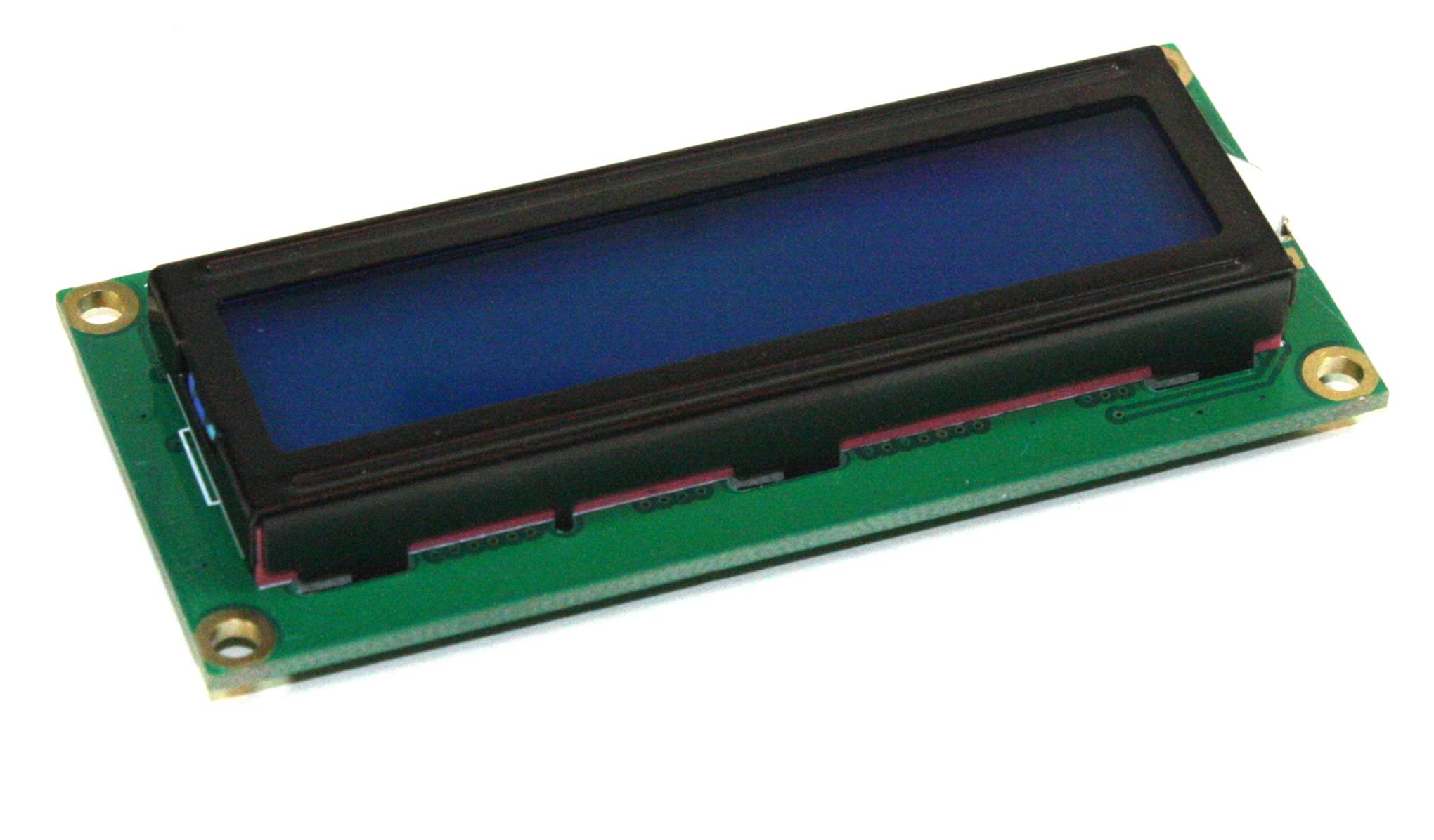
Figure 14-11. Two-line LCD display module with SPI interface
Figure 14-12. Color LCD display module with SPI interface
|
Product |
Vendor/manufacturer |
URL |
Interface |
|
1.8” color LCD display |
Adafruit |
http://www.adafruit.com |
SPI |
|
2.8” touchscreen color LCD display |
Haoyu Electronics |
http://www.hotmcu.com |
SPI |
|
3.2” touchscreen color LDC display |
SainSmart |
http://www.sainsmart.com |
SPI |
|
Table 14-8. SPI display devices |
|||
Other Peripherals
Table 14-9 lists some of the available peripheral devices with I2C and SPI interfaces (or, in some cases, both).
|
Device |
Manufacturer |
Description |
Interface |
|
ADG714 |
Analog Devices |
Eight-channel analog switch bank |
SPI |
|
ADXXRS450 |
Analog Devices |
Single-axis MEMS angular rate sensor (gyroscope) |
SPI |
|
ADXL345 |
Analog Devices |
Three-axis accelerometer |
I2C/SPI |
|
LIS3LV02DL |
STI |
Three-axis accelerometer |
I2C/SPI |
|
PCF8583 |
NXP |
Clock and calendar with 240 bytes of RAM |
I2C |
|
SAA1064 |
NXP |
Four-digit LED driver |
I2C |
|
TDA1551Q |
NXP |
2 × 22W audio power amplifier |
I2C |
|
Table 14-9. Other I2C/SPI peripheral devices |
|||
Given that there are so many types of components available with either an I2C or SPI interface, and sometimes both in the same device, the best way to find them is to look through catalogs from large electronics distributors and the manufacturer’s websites. I’ve yet to find a definitive “all-in-one” listing of available I2C or SPI peripherals, but one might exist somewhere. However, given the highly volatile and constantly changing nature of the electronics industry, trying to compile and maintain a comprehensive listing might end up being an exhausting exercise.
RS-232
SPI and I2C employ techniques that predate most modern communications methods, such as synchronous clocked serial data and unique device addressing. But SPI and I2C are intended to be used within the confines of a PCB, not as an interface to external peripheral devices.
When you need an external device to communicate with another device like a PC, the simplest choice (and the most common until recently) has been RS-232, also known officially as EIA-232 due to a change of venue for the standards association that currently maintains it. But, since this interface has been known as RS-232 for the past several decades, I’ll continue to refer to it that way here.
I think it’s worthwhile to devote some time to RS-232, and RS-485 as well (covered in “RS-485”), because these interfaces are both still in common use and they are historically significant. Many microcontrollers and microprocessors have asynchronous serial interfaces as built-in features, needing only the appropriate signal level circuits to connect them to external devices. From a historical perspective, both SPI and early versions of RS-232 have common roots in early synchronous serial technology (it wasn’t until UARTS became economically feasible that serial interfaces started dropping the clock signals). The RS-232 specification still defines a synchronous mode of operation, although no one uses it any longer (at least not that I’m aware of). The USB interface, along with some industrial interface standards, uses the concept of differential signalling employed by RS-485 and its predecessor, RS-422. If you understand RS-232 and RS-485 (in addition to SPI and I2C), you can apply that knowledge to other types of data communications, as well.
RS-232 is a voltage-based serial data interface. The difference between a logical zero and a logical one is determined by the voltage level present on the signal lines. Figure 14-13 shows how this works.
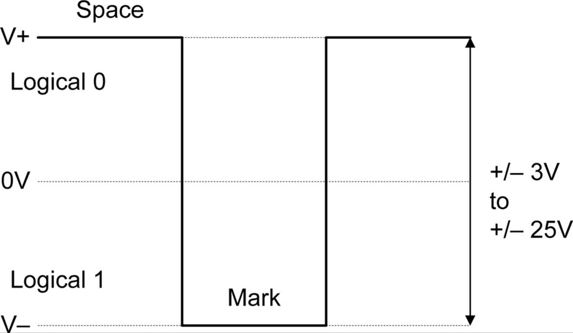
Figure 14-13. RS-232 signal voltage levels
Notice that RS-232 data signals employ negative logic; that is, a logical true or mark (1) is a negative voltage level, and a logical false or space (0) is a positive level. Also notice that RS-232 is bipolar, although some nonstandard implementations use zero volts as the mark level. Because most modern logic circuits don’t have a negative voltage available, special driver ICs are used to generate the necessary voltage levels. We’ll take a look at those later.
Never mix “real” RS-232 with the TTL-level signals found on some microcontrollers. What comes out of the back of a PC can produce a negative 12 volts, if it’s a full implementation of RS-232. This will almost certainly damage something like an Arduino or an 8051 microcontroller.
RS-232 is a full-duplex interface. It is also (usually) asynchronous, and all data clock synchronization is derived from the incoming data stream itself, not from an additional clock signal line in the interface (there is, of course, an exception to this: RS-232 can be implemented as a synchronous interface, but it is seldom used). RS-232 can be used in half-duplex mode, as well (see “Half- and Full-Duplex”).
Most RS-232 interfaces employ the ASCII (American Standard Code for Information Interchange) character encoding scheme, although the RS-232 standard itself does not specify a particular encoding technique. Data exchange over RS-232 takes the form of characters, and a character might be an actual ASCII character or just raw numeric data.
The original ASCII defined characters with only 7 bits of data. Sending 8 bits for each character wasn’t deemed necessary, since 128 possible characters can encode all the upper- and lowercase letters of the English alphabet and a host of punctuation and control characters as well. Sending only 7 bits per character also saved money, because it took less time, and time on a mainframe computer system was charged by the fraction of a second.
An RS-232 character consists of a start bit (a mark), followed by 5 to 9 data bits, an optional parity bit, and 1 or 2 stop bits (a space). Figure 14-14 shows the format for 8 data bits with no parity and 1 stop bit, and 7 data bits (true ASCII) with even parity and 1 stop bit. In both cases, the actual number of bits sent or received for each character or byte is 10 bits. Each unit of data, from the start bit to the stop bit (if used), is referred to as a frame.
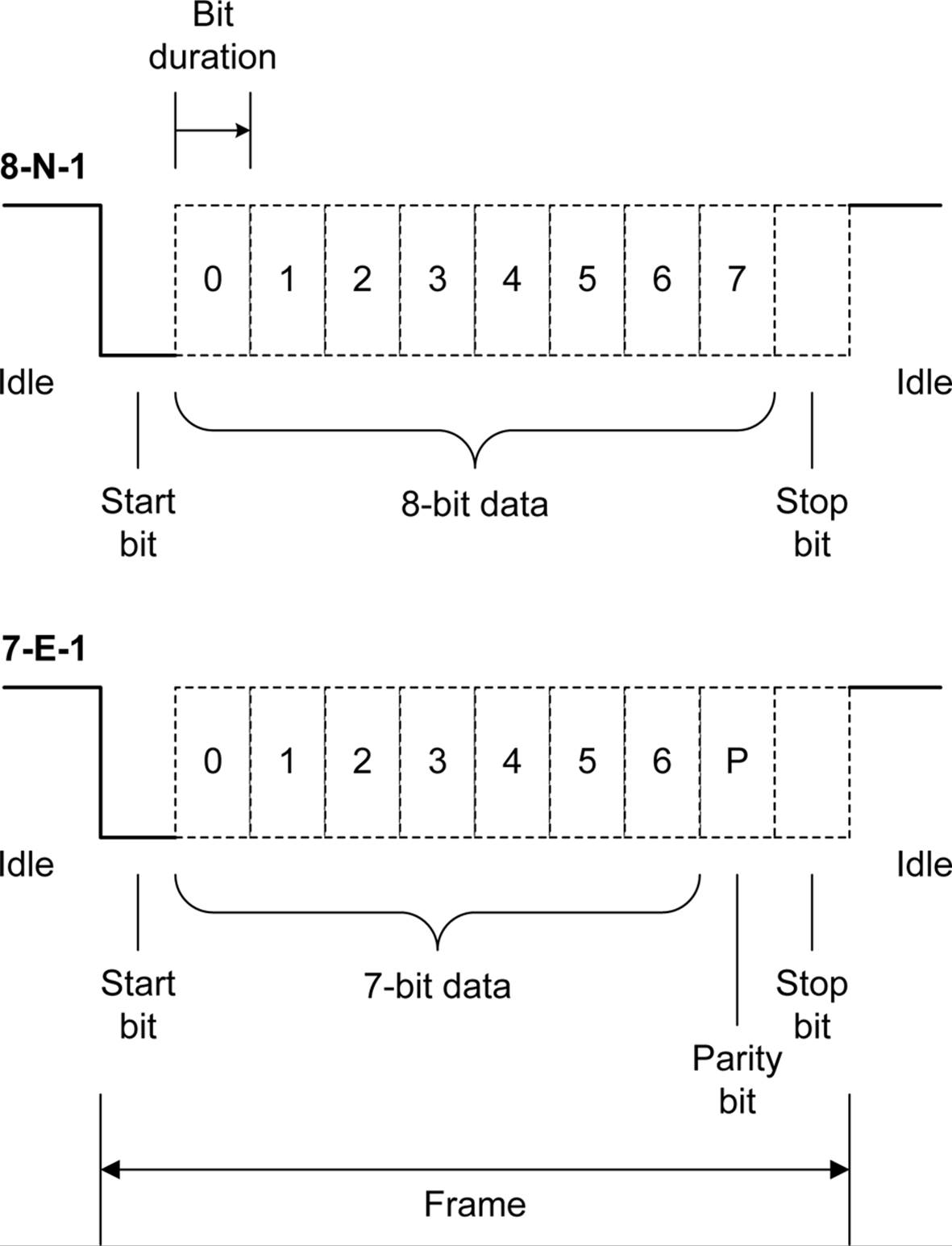
Figure 14-14. RS-232 data formats
For a specific format to work correctly, both ends of the communications channel must be configured identically from the outset. Attempting to connect a device configured as 8-N-1 to a device set up for 7-E-1 won’t work, even though both ends are sending and receiving 10 bits of data per frame. It will, at best, result in erroneous data (garbage) at the 8-bit end and a lot of parity errors at the 7-bit end.
The speed (or data transmission rate) of an RS-232 interface can be defined in terms of either characters per second or bits per second. When referring to characters per second, we use the term baud. The baud rate is the number of distinct symbols moving through a communications channel per second, whereas the bit rate is the number of discrete bits moving through a communications channel per second. In simple digital communications schemes (such as SPI) that do not use start bits or stop bits and have no concept of frames, the bit rate and the baud rate are effectively the same.
Now for an example of how the term baud is misused. When someone refers to a “9,600 baud serial data channel,” what he’s really saying is that it is a 9,600-bits-per-second channel. Many times, the term baud is used incorrectly as a synonym for bits per second. This can be blamed mostly on modem manufacturers, which I suppose felt that saying their product was a 9,600-baud device (sounds fast, right?) sounded more impressive than the more technically correct 960-characters-per-second device (doesn’t sound all that fast, does it?).
The disctinction between bit rate and baud becomes important when you are dealing with a system that might use multiple bits to represent a single symbol and any associated parity and control bits, such as the character data shown in Figure 14-14. What this means is that a serial interface running at the so-called “9,600 baud” will not send or receive 1,200 character bytes per second (9,600/8), because at least 2 of the 10 bits in the frame are taken up by the start and stop bits, so only 80% of the frame contains actual data. The actual maximum symbol rate just happens to work out to 960 characters per second in this case. As a general rule, if you know the number of bits per data frame (which will be 10 for most cases involving RS-232), then dividing the bit rate rate by that number will give you the effective transfer rate in characters per second (CPS, or true baud rate).
RS-232 has some limitations to be aware of. For example, no more than one device can be connected to a single RS-232 port on a PC or other system. In other words, it’s a point-to-point interface, as shown in Figure 14-15. It also has line length and speed limitations, because of the use of voltage swings to perform the signaling, and RS-232 tends to be susceptible to noise and interference from the surrounding environment.
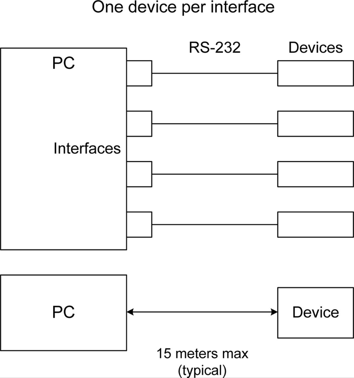
Figure 14-15. RS-232 connections
RS-232 Signals
The RS-232 interface employs a number of signals for both data transfer and handshaking between two devices. Most of these signals are from the days when RS-232 was first defined and its intended application was to connect a terminal or mainframe to a modem. External modems are becoming scarce, but most RS-232 interfaces still retain the various lines shown in Figure 14-16. Note that these are for a DB-9 type connector. There are other signal lines that might be implemented with a DB-25 connector, but they are seldom used. If you’re curious, you might want to find a copy of the EIA-232 specification and give it a read.
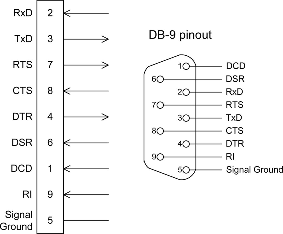
Figure 14-16. RS-232 signals
The basic RS-232 signals shown in Figure 14-16 and defined in Table 14-10 are really all that are necessary to implement a full RS-232 interface with hardware handshaking.
|
Signal |
Definition |
|
RxD |
Received data |
|
TxD |
Transmitted data |
|
RTS |
Request to send |
|
CTS |
Clear to send |
|
DTR |
Data terminal ready |
|
DSR |
Data set ready |
|
DCD |
Data carrier detect |
|
RI |
Ring indicator |
|
Table 14-10. RS-232 interface signal names |
|
In many cases, all you really need are the RxD (receive) and TxD (transmit) data lines, and some devices are indeed wired this way. The CTS, RTS, DTR, and DSR signals are useful in cases where there is a need for strict data flow control, but at baud rates of 9,600 or less, where data is not moving continuously in large blocks, they can be eliminated. The DCD and RI signals are essentially useless these days, unless you want to connect to an old-style outboard modem. However, that doesn’t mean the signals can just be left floating and unconnected. On a PC, for example, the control signals might need to be terminated correctly or the interface logic behind the RS-232 port might simply refuse to work.
DTE and DCE
When working with RS-232 interfaces, you will no doubt encounter the abbreviations DTE and DCE, which translate to data terminal equipment and data communications equipment, respectively. Hailing from the days of mainframes and acoustic coupler modems, these terms were used to define the endpoints and link devices of a serial communications channel. The terms were originally introduced by IBM to describe communications devices and protocols for their mainframe products.
In the context of RS-232, DTE devices are found at the endpoints of a serial data communications channel. The terminal in DTE does not necessarily refer to a thing with a roll of paper and a keyboard (a teletype terminal, or TTY), or a CRT and a keyboard (an old-style computer terminal, orglass TTY as they were once known). It literally means “the end.” Figure 14-17 shows this arrangement graphically.
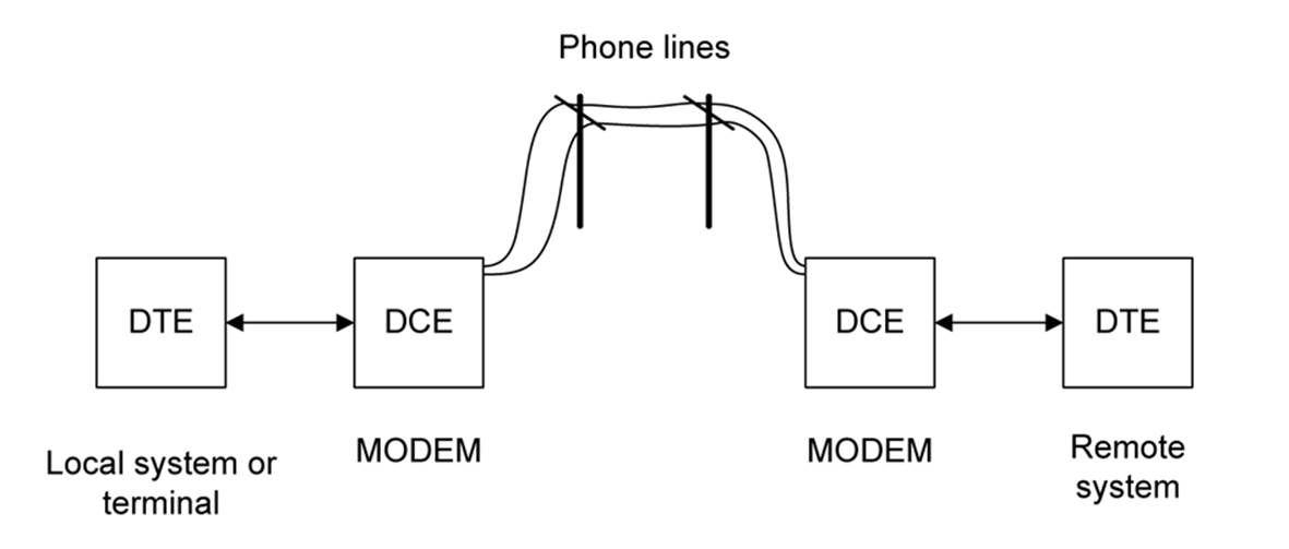
Figure 14-17. DTE and DCE
Another way to look at it is in terms of data sink and data source. A data sink receives data, and a data source emits it. Either end of the channel (the DTE devices) can be sinks or sources. The DCE devices provide the channel between the endpoints using some type of communications medium. For a system using modems as the DCE devices, this would typically be a telephone line, although VHF radio and microwave links have also been used in the role of communications medium.
Nowadays, modems are becoming something of an endangered species, although they are still used for data communications in some remote areas of the US and in places around the world that lack high-speed internet services. However, the wiring employed in RS-232 cables and connectors still reflects that legacy, which is why it’s important to understand it in order to correctly connect things using RS-232.
The signals described in the previous section are named with reference to the DTE. In other words, on a DTE device, TxD is a data source, or output. On a DCE, it is a sink, or input, for the TxD of the DTE. This also applies to the RxD line. In effect, the DCE’s data source and sink connections are functionally inverted with respect to the DTE’s TxD and RxD lines, even though they have the same name. This might seem confusing, but the upshot of it all is that when you are connecting a DTE to a DCE, the interface is wired pin-to-pin between them (1 to 1, 2 to 2, and so on).
If you need to connect two devices that happen to be DTEs, you will need to use what is called a cross-over cable, or, if you don’t need the handshake lines, a null modem cable. Figure 14-18 shows how the TxD and RxD lines would cross over for a DTE-to-DTE interface. It does not show how the handshake lines would need to be connected. For details about the use of handshaking, see “Handshaking”.
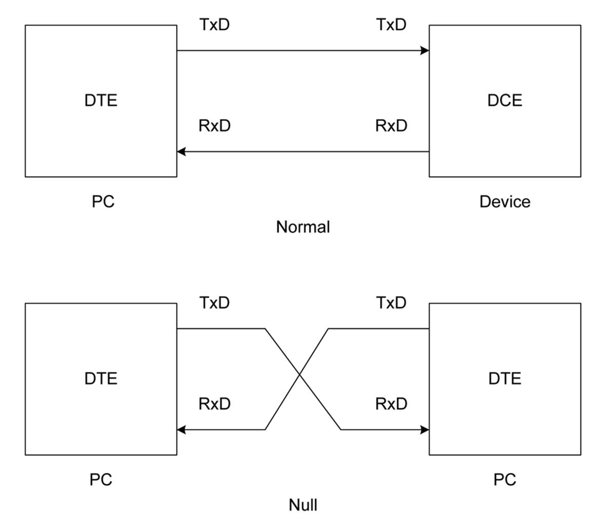
Figure 14-18. RS-232 null modem wiring
Most devices with a serial port are wired as DTE devices, although some can be configured as DCE. You can do this using jumpers, small PCB-mounted switches, a front-panel control, or even via software. The built-in serial port on a PC is typically implemented as a DTE.
Handshaking
For devices with low-speed interfaces, or when the communications protocol is strictly a command/response format, you probably don’t need the rest of RS-232’s handshaking lines. In this case, you can use a ready-made commercial null-modem cable or a null-modem adapter like the one shown in Figure 14-19.
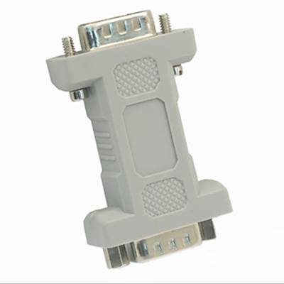
Figure 14-19. A DB-9 RS-232 null-modem adapter
RS-232’s handshaking signals originated in response to its initial usage—namely, transferring data between a terminal and a remote host mainframe computer system, sometimes via a modem. The DTR, DSR, DCD, and RI signals mainly apply to devices such as modems. The RTS and CTSsignals are used for flow control, regardless of what types of devices are involved.
In the original version of the RS-232 specification, the use of the RTS and CTS lines is asymmetric—in the sense that the DTE asserts RTS to indicate that it has data ready to send to a DCE device, and in response, the DCE asserts CTS to indicate that it is in a state to accept data from the DTE. This request/accept protocol is used with half-duplex devices like RS-232 to RS-485 convertors, where the DTE’s RTS signal is used to put the RS-485 device into transmit mode. “RS-485” covers the half-duplex RS-485 interface. Note that this asymetric flow control scheme does not provide any way for the DTE to indicate that it is unable to accept data from a DCE, so the DTE needs to be able to accept and buffer whatever the DCE throws at it.
Of course, someone developed a nonstandard version of the handshake protocol, wherein the CTS signal is used to indicate that the DCE is ready to accept data and the RTS signal indicates that the DTE can accept data. This is known as RTS/CTS handshaking. In some operating systems, enabling an RTS/CTS handshake flow control is a configuration setting.
Some RS-232 interfaces are designed to operate without the handshaking lines, while with others, the handshaking logic can be disabled by software. But even if one device doesn’t support handshaking signals, another device might, and it will need to be wired or configured to ignore them. Many people have puzzled over why an RS-232 port wasn’t working, only to discover that they needed to correctly configure the handshaking lines for the port in order to get it to respond to an external device.
Figure 14-20 shows how a microcontroller can be connected to a DB-9 connector for an RS-232 port configured as DTE. This is sometimes referred to as a handshake loop-back.
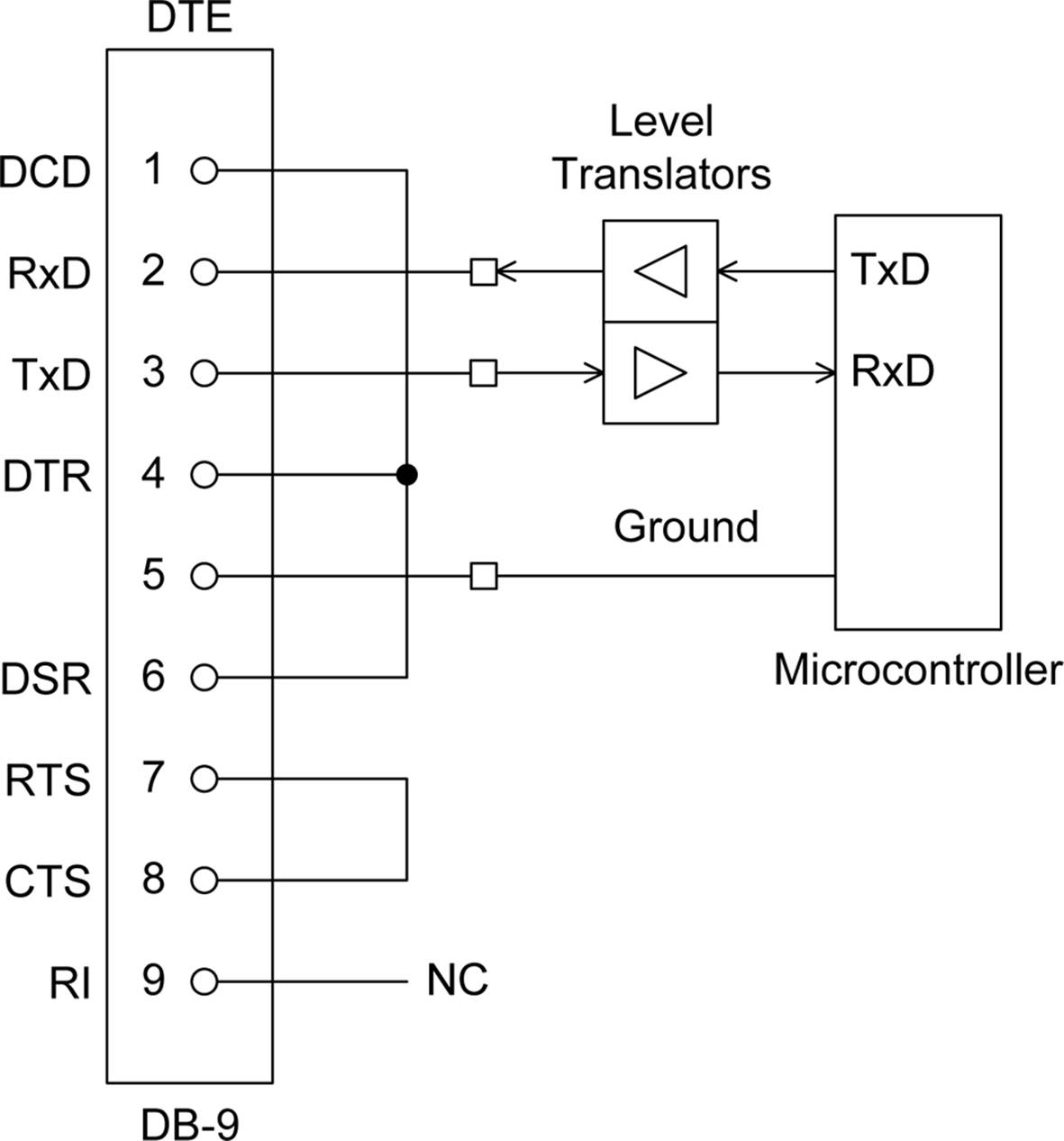
Figure 14-20. Connecting a microcontroller to a standard RS-232 port
Microcontrollers don’t come with handshaking implemented for a serial port. If handshake signals are necessary, they must be taken from general-purpose DIO pins and controlled by software.
RS-232 Components
With a microcontroller that already has a built-in UART, all you really need in order to connect it to something with an RS-232 interface are a set of level translators, also called driver ICs. These components convert 3.3V or 5V logic signals into the +/– voltages used for RS-232. Table 14-11lists some of the interface ICs that are available. Some have driver/receiver pairs (a transceiver), and others have just drivers or receivers.
|
Part number |
Manufacturer |
Transmitters |
Receivers |
|
LTC2801 |
Linear Technology |
1 |
1 |
|
LTC2803 |
Linear Technology |
2 |
2 |
|
MAX232 |
Maxim |
2 |
2 |
|
MAX232 |
Texas Instruments |
2 |
2 |
|
MC1488 |
ON Semiconductor |
4 |
0 |
|
MC1489 |
ON Semiconductor |
0 |
4 |
|
SN75188 |
Texas Instruments |
4 |
0 |
|
SN75189 |
Texas Instruments |
0 |
4 |
|
Table 14-11. RS-232 interface ICs (level translators) |
|||
External UART IC components are available from multiple sources. These aren’t generally suitable for use with microcontrollers because they require an address and data bus interface that might not be available with a microcontroller. They are commonly found along with microprocessors to provide RS-232 interface capability.
The MAX3100 or MAX3107 devices from Maxim are one type of UART IC, and Texas Instruments is a source for the venerable 16550 UART in the form of the PC16550D IC (Table 14-12 lists a few other available UART ICs). The 16550 is historically interesting, because many older (and even current) motherboards include an embedded version of this device in the IC chip set that supports the microprocessor. It might no longer be a separate outboard part in a PC, but it, or something very much like it, might still be there.
|
Part number |
Manufacturer |
Interface |
|
MAX3100 |
Maxim |
SPI |
|
MAX3107 |
Maxim |
I2C/SPI |
|
PC16550D |
Texas Instruments |
Address/data bus |
|
SC16IS740 |
NXP |
I2C/SPI |
|
TL16C752B |
Texas Instruments |
Address/data bus |
|
Table 14-12. RS-232 UART ICs |
||
RS-485
RS-485 (or EIA-485) is commonly found in instrument control interfaces and in industrial settings. RS-485 and its predecessor, RS-422, have a high level of noise immunity, and cable lengths can extend up to 1,200 meters in some cases. RS-485 is also significantly faster than RS-232. It can support data rates of around 35 Mb/s with a 10-meter cable, and 100 Kb/s at 1,200 meters.
So why should you care about RS-485? To be honest, you might not have a reason to, but as stated earlier, it does bear on the historical background of differential signaling schemes like USB. Outside of the historical curiosity aspect, should you ever want to work with things like a data acquisition module for an automated small-batch brewery, or a stepper motor controller module for that robot you’ve been wanting to build, then knowing about RS-485 might come in handy (search Jameco’s website for part number 184997).
RS-485 Signals
RS-485 owes its speed and range capabilities to the use of differential signaling. Instead of using a dedicated wire to carry data in a particular direction, two electrically paired wires can transfer data in either direction, but not at the same time. The two wires in a differential interface are always the opposite of each other in polarity. The state of the lines relative to each other indicates a change from a logic value of 1 to a 0, or vice versa. Figure 14-21 shows a typical situation involving asynchronous serial data that incorporates a start bit and a stop bit. For comparison, it also shows the digital TTL input that corresponds to the RS-485 signals.
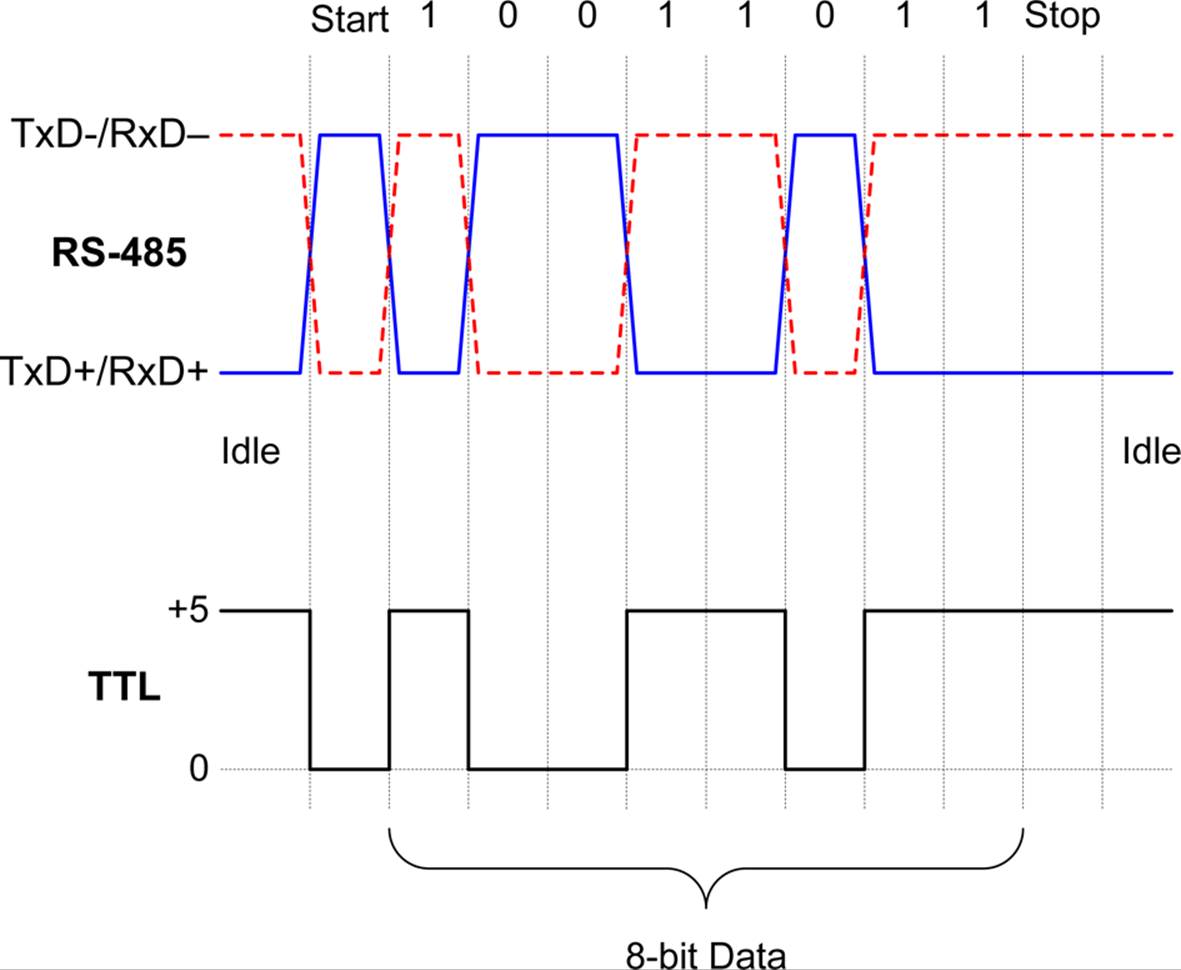
Figure 14-21. RS-485 signals
The TxD–/RxD– and TxD+/RxD+ designations in Figure 14-21 indicate that the + and – lines will connect a TxD output to an RxD input. The + and – indicate the logic true polarity of the signal (the – line is true (1) when low, and the + is true (1) when high). In many diagrams of RS-485 circuits, you will often see the lines labeled as just + and –. Note that the + and – signals always return to the initial starting state at the completion of the transfer of a byte of data.
Line Drivers and Receivers
In an RS-485 interface, each connection point uses a pair of devices consisting of a differential transmitter and a differential receiver, as shown in Figure 14-22.
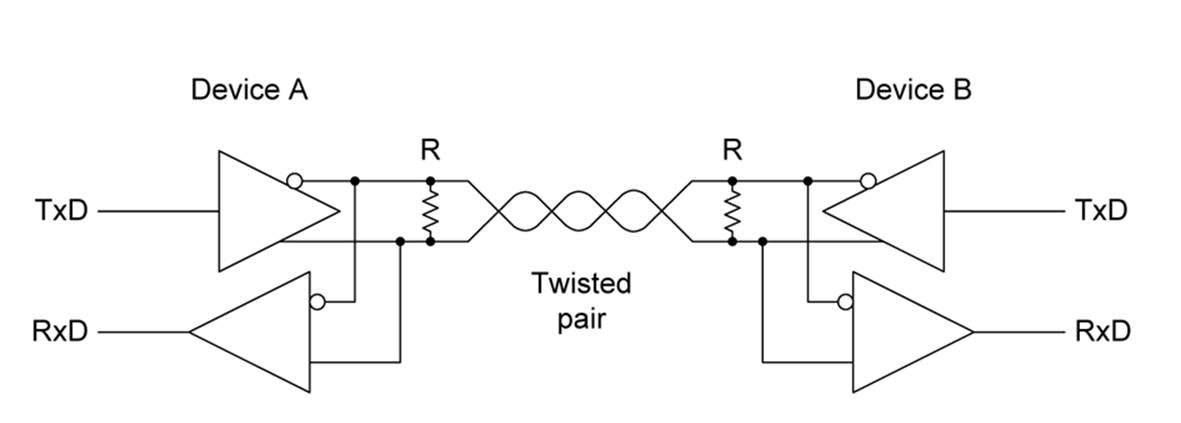
Figure 14-22. RS-485 differential transmitter and receiver
RS-485 might be implemented as a two-wire half-duplex interface, or it might be a bidirectional, four-wire, full-duplex interface, but for many applications, full-duplex operation is not required. Figure 14-23 shows a four-wire arrangement.
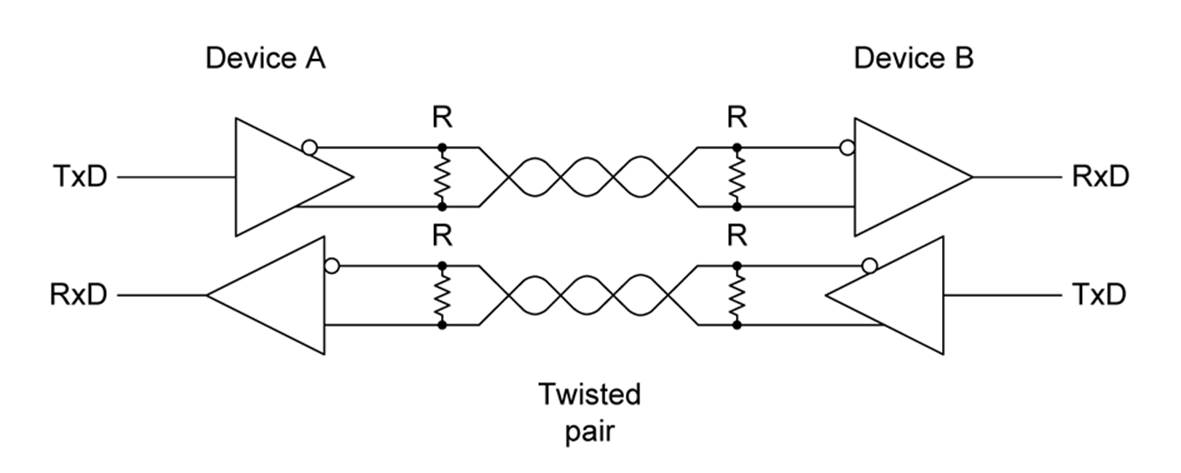
Figure 14-23. RS-485 full-duplex four-wire interface
RS-485 Multi-Drop
RS-485 also allows you to connect more than one device (or node) to the serial bus in what is called a multi-drop configuration, as shown in Figure 14-24. To do this, you must be able to place the transmitter (output) section of an RS-485 driver into a Hi-Z (or high impedance) mode. This capability is also essential when RS-485 is connected in two-wire mode.
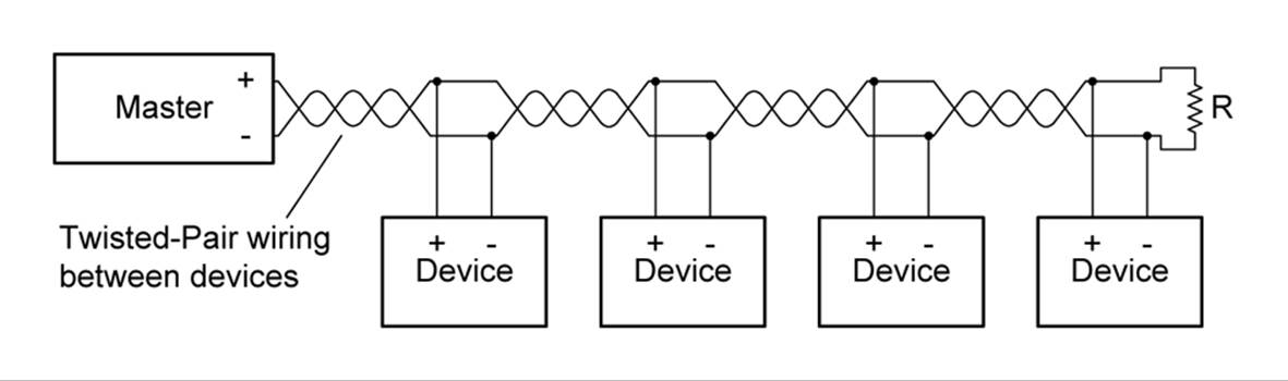
Figure 14-24. RS-485 multi-drop connections
The reason for this is that, if the transmitter were always actively connected to the interface, it could conflict with another transmitter somewhere along the line. In Figure 14-25, you can see how the drivers take turns being talkers (or data sources) when wired in half-duplex mode, depending on which direction the data is moving. There is really no need to disconnect the receivers, so they can listen in to the traffic on the interface at any time.
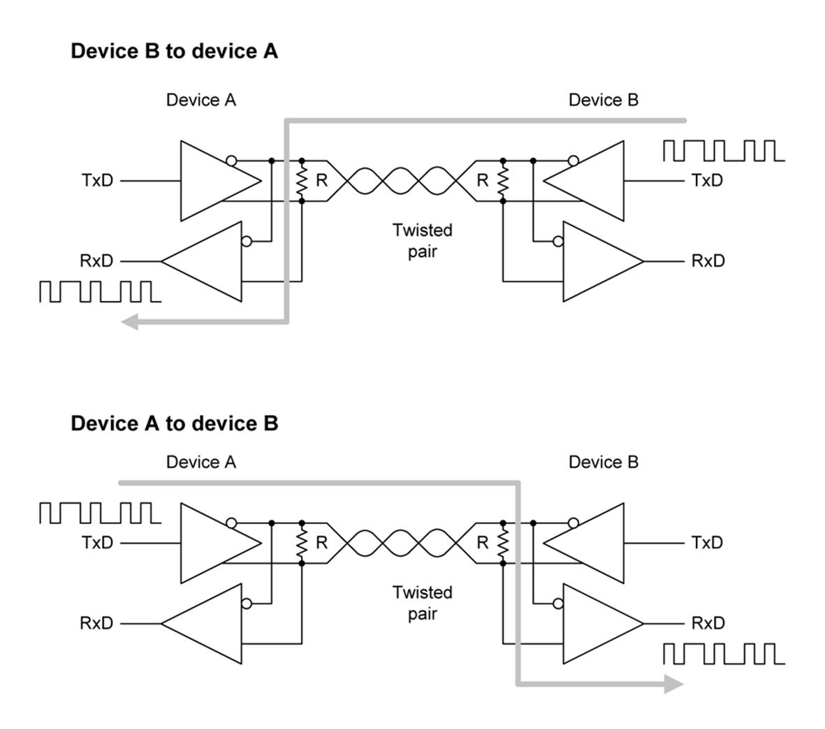
Figure 14-25. RS-485 half-duplex mode operation
In a typical multi-drop configuration, one device is designated as the controller (or master) and all other devices on the RS-485 bus are subordinate to it, although it is possible to have multiple controllers on an RS-485 network. The default mode for the controller is transmit, and for the subordinate devices, it is receive. They trade places when the controller specifically requests data from one of the subordinate devices. When this occurs, it is called turnaround.
When using a half-duplex RS-485 interface, you must take into account the amount of time required to perform a turnaround of the interface. Even with an interface that can sense a turnaround electronically and automatically change its state from sender to receiver, there is still a small amount of time involved. Some RS-232 to RS-485 converters can use the RTS line from the RS-232 interface to perform the turnaround, as well.
RS-485 Components
There are numerous transceiver ICs available for use with RS-485, as listed in Table 14-13. Many are available in through-hole DIP packages, but many are packaged in small-outline SMD styles, which are relatively easy to solder onto a PCB.
|
Part number |
Manufacturer |
Number of Transceivers |
|
SN65HVD11DR |
Texas Instruments |
1 |
|
MAX13430 |
Maxim |
1 |
|
MAX13442E |
Maxim |
1 |
|
SN75ALS1177N |
Texas Instruments |
2 |
|
SN65LBC173AD |
Texas Instruments |
4 |
|
Table 14-13. RS-485 transceiver ICs |
||
Some of the parts listed in Table 14-13 are designed to operate in 3.3V circuit. Others can tolerate from 3.3 to 5V logic levels. If you elect to use an RS-485 transceiver IC, be sure to read the datasheet. Some have coupled logic for half-duplex operation. Other have TxD/RxD driver/receiver pairs that are not internally linked, so they can be used for full-duplex operation.
RS-232 vs. RS-485
Table 14-14 shows a comparison of some of the electrical characteristics of RS-232 and RS-485.
|
Characteristic |
RS-232 |
RS-485 |
|
Differential |
No |
Yes |
|
Max number of transmitters |
1 |
32 |
|
Max number of receivers |
1 |
32 |
|
Modes of operation |
Half- and full-duplex |
Half- or full-duplex |
|
Network topology |
Point-to-point |
Multi-drop |
|
Max distance |
15 m |
1,200 m |
|
Max speed at 12 m |
20 Kbs |
35 Mbs |
|
Max speed at 1,200 m |
n/a |
100 Kbs |
|
Table 14-14. Comparison of key features of RS-232 and RS-485 |
||
In general, RS-232 is fine for applications that don’t require high speed and with cable lengths shorter than 5 meters (about 15 feet) or so. If an external device utilizes very short (2- to 10-character) commands, returns equally short responses, and sometimes takes significantly longer to perform the commanded action than the time required to send the command to the device, an RS-232 interface at a speed of 9,600 baud is perfectly acceptable. In other cases, such as when you might want to have sensors or controllers distributed on a single communications bus, RS-485 would be the way to go for a serial data interface.
USB
USB was intended to be easy for end users to deal with. Consequently, when you are connecting a digital camera, tablet, or a BeagleBone board to a PC using a USB cable, all the details about the connection are hidden. Things like connection speed and capabilities are contained within both the external device and the driver software running on the user’s computer. After the driver software is installed, the user need only plug in the device to start using it. But this ease of use for the user comes at the price of complexity for the person implementing the USB interface and the driver software.
Some microcontrollers come with built-in USB logic, and in other cases, you might need or want to add USB capability by using an outboard interface IC. It is also possible to convert RS-232 or TTL-level serial data into USB and back again using a single IC. In general, however, if the thing you are working with doesn’t already have USB, then adding it should probably involve some careful thought. It might not be as simple as you think, because even if the hardware is straightforward, you will still need to create or buy the software to communicate with it. From a developer’s or engineer’s point of view, USB can be a challenge to work with.
If you plan to work with USB, you should be prepared for something of a steep learning curve. USB is not a simple protocol, and there is a lot going on behind the scenes to make it all work as seamlesslty as it does—at least most of the time.
This section is not a complete description of how to implement or use a USB interface. That can easily take an entire book, such as some of the titles listed in Appendix C. The intent here is give you some idea of what is involved and provide some suggestions for places to look for the additional details you might need.
USB Terminology
As is true of almost every other specialized area of electronics technology, there are words and terms unique to USB technology. For convenience’s sake, here are some of the terms used with USB that will appear in the rest of this section (they are also in the Glossary):
Data sink
A place where data is received.
Data source
A source of data (i.e., a sender).
Descriptor
A data structure within a device that allows it to identify itself to a host.
Device
A USB peripheral or function. Also used as peripheral device. See function.
Downstream
Looking out from the host to hubs or devices connected outward on a USB network.
Endpoint
An endpoint exists within a device, typically in the form of a FIFO buffer. They can be either data sinks (receiving) or data sources (sending).
Enumeration
When a USB device is initially connected to host, the host gets a connection notice and proceeds to determine the type and capabilities of the device.
Function
A function is a USB device, also referred to as a USB peripheral or just device. USB functions are downstream from the host.
Host
The host is the master on a USB network, and all other devices (or functions) respond to it.
Hub
A USB hub is used to expand the number of devices with which a USB host can communicate.
Interface
A set of endpoints in a device that act as either data sources or data sinks. An interface can have multiple endpoints acting as data sinks or data sources.
Peripheral
Another name for a device or function.
Pipe
A logical connection between a host and the interface endpoints of a device.
Request
Sent by a host to a device to request data or have the device perform an action.
Upstream
Looking back toward the host from the perspective of the hubs and devices in a USB network.
USB Connections
USB is a half-duplex asynchronous serial interface that uses a master/slave type bus with exactly one master and multiple slaves. The slaves are called devices, peripherals, or functions. The master is called a host, and only the host can initiate USB transfers. Peripheral devices always respond; they never initiate.
Electrically, USB is simple: just four wires. As shown in Figure 14-26, two of the wires carry data and use a differential signaling method similar to RS-485. The other two wires are used for DC power and ground. All four lines run through a shielded cable. Chapter 7 describes the connectors used for a host (an A type) and a device (B, mini, or micro).
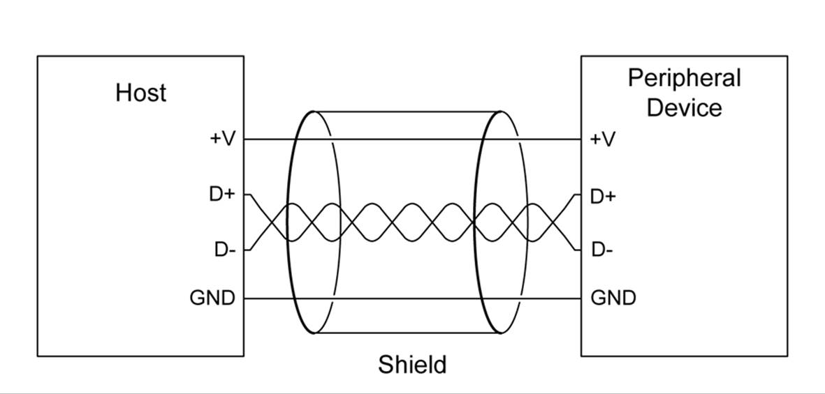
Figure 14-26. USB electrical wiring
A USB host can detect the devices connected to it and query each one to enumerate their type and capabilities. It can also detect when a device is connected or removed. Multiple USB devices are connected in a tree-like topology, with the controller at the base of the tree and the individual USB devices out at the branch tips. A USB hub is used to distribute signals between one controller port and multiple device ports. Figure 14-27 shows a USB network consisting of a host system with an internal hub, two external hubs, and eight USB devices.
USB Classes
The USB standard defines various classes of devices that utilize a USB interface. Each class has its own set of commands and responses, and each is intended for a specific set of applications. Table 14-15 lists some of the more common classes that you might encounter on a regular basis.
|
USB class |
Example(s) |
|
Communications |
Ethernet adapter, modem |
|
HID (Human Interface Device) |
Keyboard, mouse, etc. |
|
Imaging |
Webcam, scanner |
|
IrDA |
Infrared data link/control |
|
Mass Storage |
Disk drive, SSDD, flash memory stick |
|
PID (Physical Interface Device) |
Force feedback joystick |
|
Printer |
Laser printer |
|
Smart Card |
Smart card reader |
|
Test & Measurement (USBTMC) |
Test and measurement devices |
|
Video |
Webcam |
|
Table 14-15. Common USB device classes |
|
You are probably already familiar with the HID and Mass Storage classes. These two classes include things like keyboards, mice, simple joysticks, outboard USB disk drives, and flash memory sticks (so-called thumbdrives). The HID class is relatively easy to implement, and most operating systems come with generic HID class drivers, so it is not uncommon to find devices implemented using the HID class that don’t look anything at all like a keyboard or mouse. If a USB device uses a unique interface, it is up to the implementor to supply the low-level interface drivers needed by the operating system.
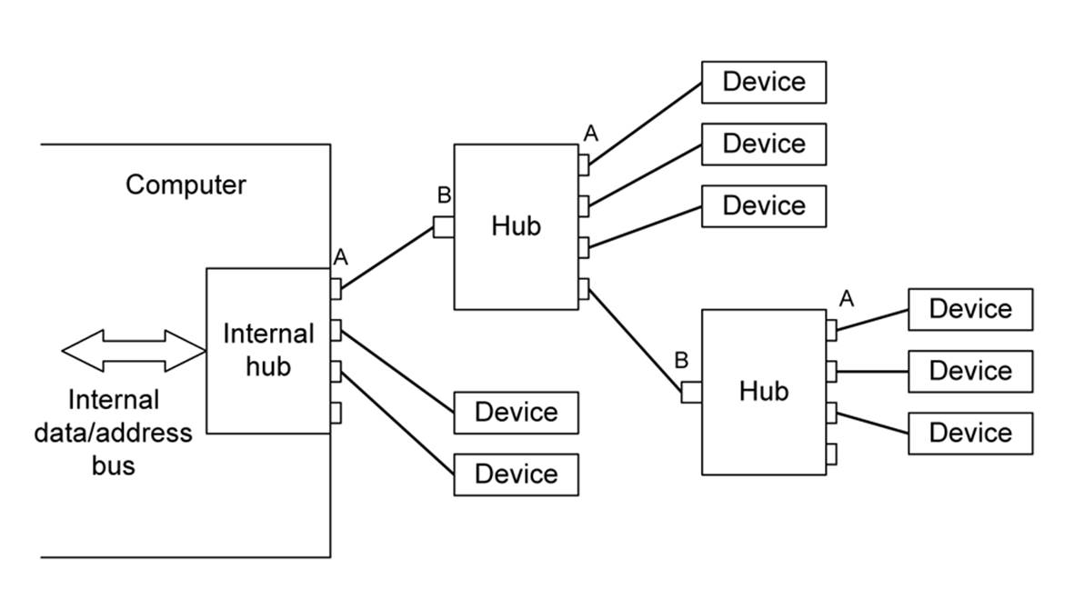
Figure 14-27. Multiple USB connections with hubs
USB Data Rates
The maximum data rate for a USB interfaces (measured in bits per second) can vary from 1.5 Mb/s to 4 Gb/s. The data transfer rates for USB are defined in terms of a revision level of the USB standard. In other words, devices that are compliant with USB 1.1 have a theoretical maximum data rate of 12 Mbits/s (megabits/second) in the full-speed mode, whereas USB 3.0-compliant devices have a maximum data transfer rate of 4 Gb/s (gigabits/second). Table 14-16 lists the specification levels and the associated maximum data transfer rates.
|
Version |
Release date |
Maximum data rate(s) |
Rate name |
Comments/features added |
|
1.0 |
1996 |
1.5 Mb/s |
Low speed |
Very limited adoption by industry |
|
1.0 |
1996 |
12 Mb/s |
Full speed |
|
|
1.1 |
1998 |
1.5 Mb/s |
Low speed |
Version most widely initially adopted |
|
1.1 |
1998 |
12 Mb/s |
Full speed |
|
|
2.0 |
2000 |
480 Mb/s |
High speed |
Mini and micro connectors, power management |
|
3.0 |
2007 |
4 Gb/s |
Super speed |
Modified connectors, backward compatible |
|
Table 14-16. USB versions |
||||
USB 3.0 is still rather new, and most USB devices that one might encounter in use will either be 1.1 or 2.0 compliant. You should also know that even though a device claims to be a USB 2.0 high-speed type, the odds of getting sustained rates of 480 Mb/s are slim. The time required for the microcontroller in the USB device to receive a command, decode it, perform whatever action is requested, and respond back to the host can be considerably slower than what you might expect from the data transfer rate alone. In addition, the ability of the host controller to manage communications can contribute to slower than theoretical maximum data rates. If the host is busy with other tasks, it might be unable to service the USB channel fast enough to sustain a high data throughput.
USB Hubs
A USB hub concentrates and passes data from downstream devices and other hubs to the upstream host. A root hub will pass the data directly into the host system. A PC (and most computers with USB capability) typically has a root hub built into its USB controller logic. Besides serving as the first-order router/distribution controller for a USB network, the root hub also detects when devices are being connected or disconnected. A root hub can be implemented either as a separate IC or as part of the chip set for the computer’s microprocessor.
How USB devices and hubs are connected can also play a big part in how responsive the communications will be. A USB network using v1.1 hubs and devices is only as fast as the slowest device in the network, so just one 1.5 Mb/s device will drag the enter network down to that speed, even if some of the other devices can run at 12 Mb/s.
USB v2.0 hubs deal with this by separating the v1.1 low-/full-speed traffic from the v2.0 high-speed data. When purchasing new USB components, you should avoid v1.1 hubs and stick to v2.0 units. That way you can avoid having a high-speed v2.0 device run into a bottleneck due to v1.1 devices on your USB network, assuming that the host controller is itself USB v2.0 high-speed capable.
Hubs also participate in power management for peripheral devices. In a PC, the root hub can supply 500 mA of 5V power per A type connector. Of that, 100 mA is allocated to an external hub, leaving 400 mA for peripheral devices. A bus-powered hub is limited to 100 mA per type A port, so unless a downstream hub has its own power supply (i.e., it’s a self-powered hub), the number of devices it can support at 100 mA each is limited to four. If it’s self-powered, each of the hub’s type A ports should be able to supply 500 mA.
Device Configuration
When a device (perhaps an MP3 player or an Arduino, for example) is connected to a host, the first thing that happens is that the host becomes aware of the device due to a pull-up resistor on one of the data lines inside the device. Once a device is detected, the host requests a series of descriptors from the new device. These are data structures (tables) that contain information about the device’s class, endpoints, and speed.
The sequence of actions that result when a device is connected, and which lead up to it being fully operational and ready for use, can be summarized as follows:
1. A device is connected to a USB host or hub and a data line is pulled high by the device.
2. Host issues a reset to the new device to place it into a known state with the default address of 0.
3. Host sends a request to endpoint 0 on device address 0 to get the maximum data packet size.
4. Host might send the reset command again and then issue a Set Address command that specifies a unique address for the device at address 0. If successful, the device assumes the new address.
5. Host sends query commands to the device at the assigned address to obtain information about the device, including the Device Descriptor, Configuration Descriptor, and String Descriptor.
6. Once the host has gathered sufficient information from the device, it will load the appropriate device driver.
7. The host now issues a Set Configuration command to the device, and it will now respond to commands specific to the type of device it happens to be.
If the data received from the device is consistent and complete, the host configures the device for operation. However, if the host is not satisfied with the data obtained from the device, it will ignore the device. When this happens, the host operating system will usually open a small error window stating that it encountered a problem with the new device.
USB Endpoints and Pipes
Each USB peripheral has a unique address on the USB network, assigned by the host. Each USB device has an interface that will respond to this address, and an interface can contain up to 16 endpoints. An endpoint can be either a data source or a data sink, which is the direction of the endpoint. Each endpoint is assigned a number from 0 to a maximum of 15. Every device has a default control endpoint 0, which is bidirectional. A USB endpoint is somewhat like the notion of a port used for network communications.
Endpoints are part of a device, not something the host assigns. A device reports its endpoint numbers and characteristics when it is enumerated by the host during the initalization and configuration sequence. Once the host knows the endpoints, it uses both the device address and the endpoint number when communicating with a device. Figure 14-28 shows how endpoints exist in a device behind its assigned device address.
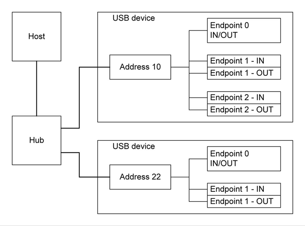
Figure 14-28. Endpoints in a USB device interface
A USB device sends and receives data using endpoints; the host client software transfers data through pipes. A pipe is a logical connection between the host and endpoint(s). Each instance of a pipe has a set of parameters associated with it, such as allocated bandwidth, transfer type (Control, Bulk, Iso, or Interrupt), data direction, and maximum packet and buffer sizes. Figure 14-29 illustrates the concept of a pipe.
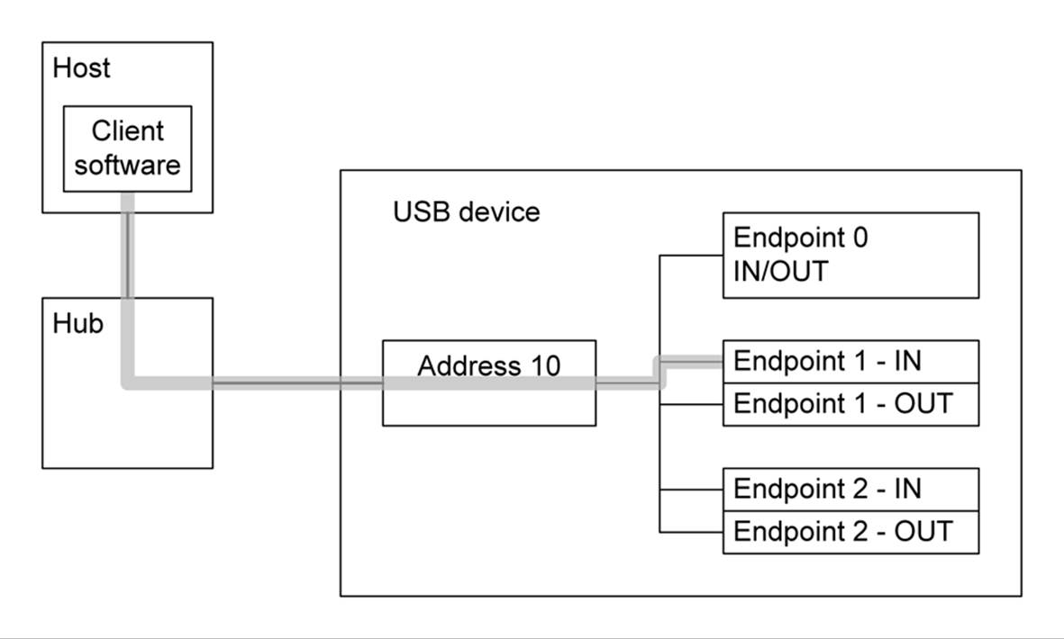
Figure 14-29. USB pipe
The USB specification defines two types of pipes: stream and message. A stream has no defined format, and it can be used to send or retrieve any type of data. A stream pipe can be used with bulk, isochronous, and interrupt transfer types, and it can be controlled by either the host or the device. Message pipes use a format defined in the USB specification, and they are always host-controlled. The direction of data flow is set by the request from the host. Message pipes support control transfers only.
Device Control
All USB devices must recognize and respond to the basic set of control commands (i.e., requests) used to enumerate devices and their capabilities. Specific requests sent by the host to a USB device will depend on the class of the device. For example, HID devices use a different set of requests than devices in the mass storage class.
Working through the possible requests and responses for each of the USB classes is way beyond the scope of this small section. I will say, however, that HID is relatively straightforward, which is why it is so often used for things like toy rocket launchers or dancing robots—and, of course, keyboards and mice. If you are working with something like a Raspberry Pi or a BeagleBone, you should have access to documentation on the USB port. If you don’t have any documentation about the device you want to connect to with a USB cable, you will have to either search it out online, if it exists, or resort to reverse-engineering. See “USB Hacking” for some tips and hints on reverse-engineering a USB interface.
USB Interface Components
Low-level components provide the interface functions necessary to implement either a host or a device, and some are capable of doing either function. Table 14-17 lists some of the IC components available for SPI to USB, I2C to USB, and RS-232 to USB.
|
Part number |
Manufacturer |
Function |
Interface |
|
CP2102 |
Silicon Labs |
USB to serial UART bridge |
RS-232 |
|
CP2112 |
Silicon Labs |
HID_ USB to I2C bridge |
I2C |
|
FT232R |
Future Technology Devices International (FTDI) |
USB to serial UART bridge |
RS-232 |
|
MAX3421E |
Maxim |
Peripheral/host controller |
SPI |
|
MAX3420E |
Maxim |
Peripheral controller |
SPI |
|
Table 14-17. USB interface ICs |
|||
You should carefully study the datasheets and reference documentation provided by the various IC manufacturers. While electrically simple, some of these devices are internally complex and require you to have a good knowledge of USB to be able to use them correctly.
USB Hacking
A while back, someone came up with the idea of making a foam “rocket” launcher as a desk toy for bored office workers. You may have seen one, or been attacked by one (it doesn’t hurt; it’s just surprising and somewhat annoying). These toys use a USB interface to control the motion of the turret and an air puff mechanism that launches the foam missile across the room. Some recent versions even have a built-in video camera to assist with aiming. Now, what if you wanted to repurpose the turret mechanism for some other task? How does the USB interface work? What are the command codes? Without technical information from the manufacturer, you are basically starting from zero.
When you’re faced with a USB interface and no documentation, sometimes the only way to find out what commands it accepts and how it responds is to reverse-engineer it. If you are adept with software development tools, you might want to take the approach described in an article by Pedram Amini.
Another way to do this involves a USB communications analyzer that can watch the data traffic moving between a USB host and a device. As it turns out, Linux has this ability already built in, but of course that means that whatever you are trying to analyze must already have software for it running under Linux. It basically involves the kernel debug module, debugfs, and the usbmon facility. The Mengazi blog has a post with more information on the topic, and the Dlog blog outlines more approaches.
There are a number of USB software diagnostic tools for different platforms available, some of them starting at free and then going up from there. Of course, expect the “free” software to have some limitations, but it might be sufficient to show you the commands and responses moving between your PC and the external device.
For an example of what can be done once the requests and responses for a device are known, check out Karl Ostmo’s controller application for the Dream Cheeky USB missile launcher for Linux called pyRocket.
Ethernet Network Communications
Ethernet is now over 30 years old. From its humble beginnings as a coaxial cable strung from computer to computer, it has evolved into a widespread form of computer networking that incorporates firewalls, routers, switches, bridges, and protocol translators into its architecture. In addition to the obvious locations like PCs, servers, and printers, Ethernet can be found in applications as diverse as industrial control systems, submarines, kitchen appliances, and traffic control systems.
Ethernet Basics
A complete description of Ethernet and networking is way beyond the scope of this book, but this section will focus on some key points to consider that might help make things clearer. For more information, refer to the texts listed in Appendix C.
But first, there’s one very important thing to remember: Ethernet is the physical transport. The Internet protocol (IP) network—with its IP addresses, sockets, and subnets—is a logical construct that can use Ethernet to move data around. Sometimes, you might hear someone refer to these two concepts as if they were the same thing. They are not. Instead of Ethernet, the transport could just as easily be RS-232, RS-485, token ring, a radio link, lasers, or some other hardware communications scheme. The IP network uses the concept of IP addresses to route data between devices on the network, but it’s doing this at a high level. At the transport level of physical wires and radio waves, data is moved from one point to another via unique hardware addresses, and that’s all it does. It’s up to the network software in the host system to process and manage the data packets. This section focuses on Ethernet and the IC components and modules available to work with it.
For the purposes of this discussion, the term device refers to the physical interface hardware and host refers to the system (PC, microcontroller, etc.) that is using the device to communicate. Hopefully, this will keep things consistent with the rest of this chapter. You might also encounter the abbreviation NIC, which stands for network interface controller. It appears quite often when you’re working with PCs, and some folks might think it means “network interface card,” but it’s actually a general concept that applies to any device that can act as an Ethernet transceiver.
Modern (10BASE-T and up) Ethernet is a full-duplex, packet-based network with no masters and no slave devices. Any Ethernet device can communicate with any other device with which it can establish a connection in a peer-to-peer manner. But in order to establish that connection and exchange data packets, the two devices need to have fixed addresses.
Every device on an Ethernet network has a media access control (MAC) address, which is a unique identification number assigned to each device. Sometimes, this number is written into a device when it’s manufactured, and other times, you need to assign it yourself. Without this identifier, an Ethernet device cannot send or receive packets of data through the network. Don’t confuse the MAC address with the IP address of a host. As stated earlier, they belong to different levels of the network, although they are used together to correctly route data packets through the network.
Ethernet is a packet-based network scheme. An Ethernet packet is called a frame and consists of seven different data fields, as shown in Figure 14-30. Frames are specified in terms of octets, which are defined as 8 bits of data. The term octet was originally used because the size of a byte on early computer systems could vary, depending on the architecture of the computer. These days, the size of a byte has settled down to 8 bits, so byte and octet are synonymous.
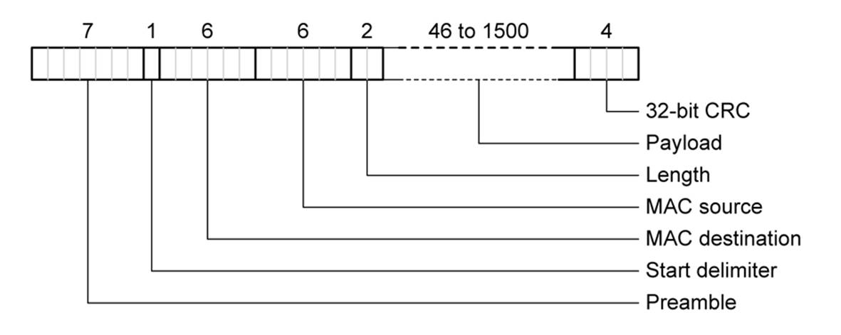
Figure 14-30. Ethernet frame contents
Figure 14-30 is the original Ethernet frame, and it’s still in widespread use. There are also variations, depending on the Ethernet specification in use. One variation in common use is known as Ethernet II. IPv6, which is very slowly replacing the original IPv4, also has its own Ethernet frame definition. Generally, you don’t need to worry about it, because the NIC will identify the variations it can handle and process them accordingly.
When considering the speed of an Ethernet connection, you might encounter terms like 10BASE-T. This translates to “10 MHz twisted pair.” In earlier versions of Ethernet, the designations 10BASE2 and 10BASE5 also appeared, referring to coaxial cables interfaces. These are now obsolete, having been replaced by the common CAT-5 and CAT-6 cables with internal twisted-wire pairs and RJ-45 connectors.
There are three network speeds in common use today, as shown in Table 14-18.
|
Network |
Speed |
|
10BASE-T |
10 MHz |
|
100BASE-T |
100 MHz |
|
1000BASE-T |
1 GHz |
|
Table 14-18. Ethernet network speeds |
|
The theoretical maximum possible speed of an Ethernet connection is measured in bits per second, which is the same as the frequencies listed in Table 14-18. Because of the overhead associated with the frame headers and the additional layers of header data used by an IP network, buffer latencies, and various processing actions, the actual number of bytes per second that can be transferred between applications running on separate hosts isn’t the same as simply dividing the speed by 8. Also keep in mind that, just because an Ethernet NIC is rated for 10 MHz, that doesn’t mean that the device using it to communicate needs to shovel data into it that fast. The NIC will send a packet when the packet is ready, and if it takes a few hundred milliseconds for a microcontroller to write enough data to fill the frame payload, then a packet will be sent every few hundred milliseconds.
To ensure backward compatibility, the typical 100BASE-T interface can slow down to accommodate a 10BASE-T connection, and a 1000BASE-T interface can (or at least should) work with a 100BASE-T or a 10BASE-T connection. Because of this, you will often see network speeds given as 10/100, or 10/100/1000. Most new PCs, notebooks, and netbooks come with built-in 10/100 Ethernet ports. Some computer and tablet products don’t have an Ethernet port, but these either rely solely on a wireless connection (discussed in “802.11”), or, if wireless is not an option, you can use a USB-to-Ethernet or Thunderbolt-to-Ethernet adapter.
Twisted-pair Ethernet is point to point, meaning that one host with one interface can connect to only one other Ethernet interface and the connections are one to one between the connectors. Because of this, you can’t simply connect one host system to another (unless one of the NICs can sense which wires are the TxD pair and which are the RxD). Generally, in order to connect one host NIC to another, you need to use a crossover cable that swaps the positions of the TxD and RxD pairs inside the RJ-45 connector.
Hubs and switches are used to expand the network. A hub is a device that accepts Ethernet packets from a host and redistributes them to every other host that happens to be connected to the hub, as shown in Figure 14-31.
Figure 14-31. Ethernet hub
A network switch is essentially a “smart” hub, in that it will discover the MAC addresses of the devices connected to it and send only the data packets with the appropriate MAC address to the intended recipient. Some switches can be configured to distribute network traffic only from certain hosts to a specific host or group of hosts. Figure 14-32 shows a simplified diagram of an Ethernet network switch.
Figure 14-32. Ethernet switch
When a host receives a packet, the network interface hardware checks the MAC address in the packet to verify that it matches the interface’s own MAC address. If it’s a match, the interface will pass the data on to the driver software in the host, where the packets are reassembled into a form that the application software even further on up the chain can deal with. Figure 14-33 shows a simplified diagram of the entire network stack.
Once past the interface hardware, we’re no longer working with Ethernet. As discussed earlier, Ethernet is just one way to move data around in a network; it’s just the transport method. Past the network interface, it’s just network data, regardless of how it got there.
From the perspective of the operating system on a computer, the network interface is a source or sink for data. The low-level software drivers that communicate with the hardware inspect the IP address of the data and pass the data to application software that has opened a port to the network interface.
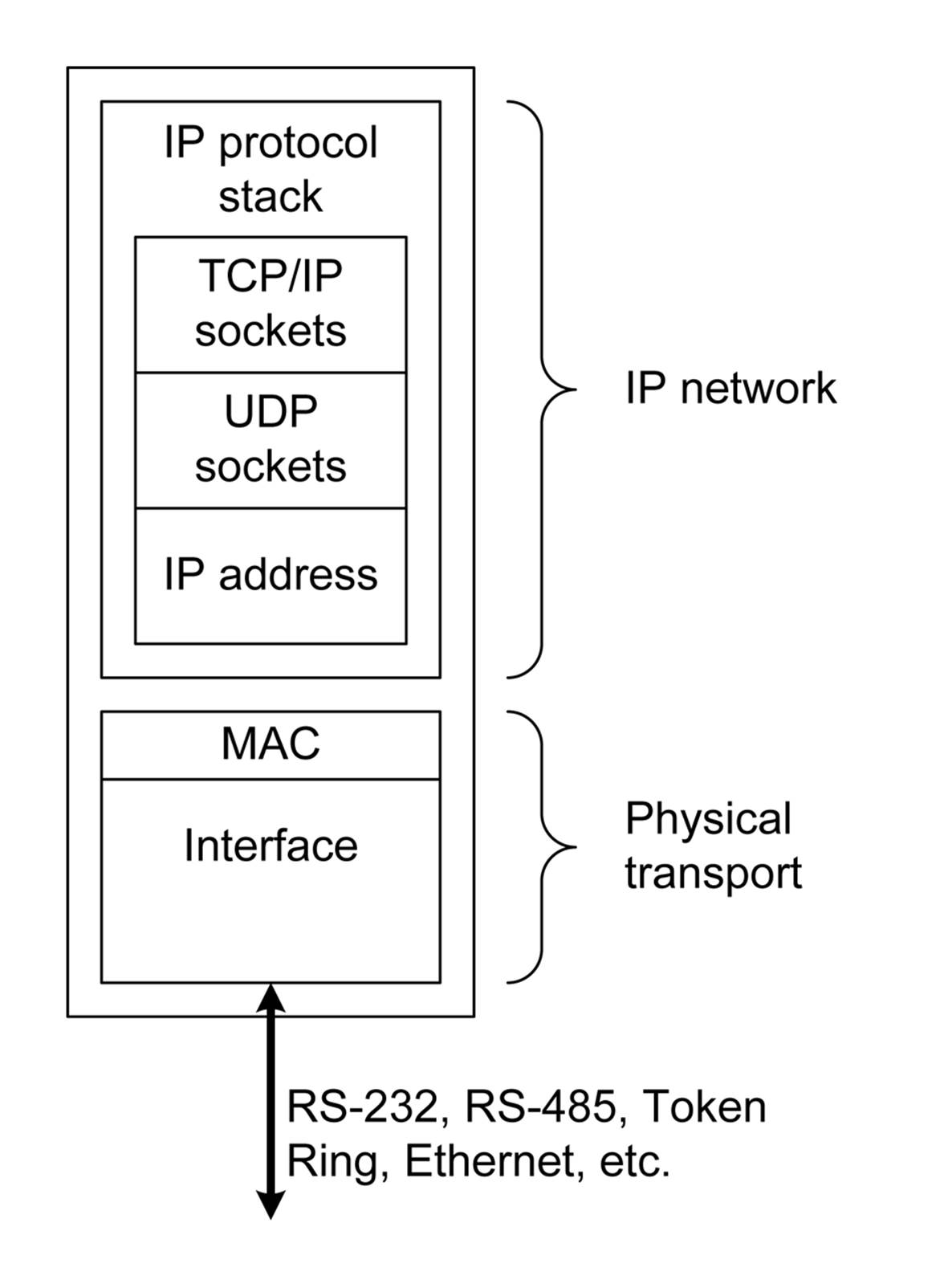
Figure 14-33. Ethernet and the IP network protocol stack
The notion of a port is similar to the endpoints used in an I2C network. They are logic constructs that allow an interface to send and receive data on behalf of multiple applications running in the system. Unlike I2C endpoints, a IP network port is bidirectional and full duplex. Figure 14-34shows how the higher-level IP network functions in a host system use the low-level Ethernet transport to move data between systems.
The low-level software that does the receiving, reassembly, assembly, and sending is called a protocol stack. Some Ethernet controller ICs have a protocol stack already built into them, while others need a microcontroller to handle it. When a host system sends data to another host, it uses the functions in the protocol stack to assemble the outgoing packet. The IP address of the remote host is used to look up its MAC address and load the Ethernet frame payload with data. When the outbound packet is complete, it is passed into the Ethernet interface for transmission.
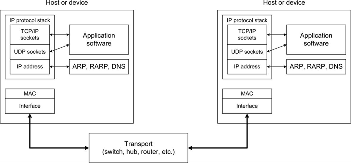
Figure 14-34. Ethernet and IP network components
Figure 14-35 shows an example network composed of six hosts, a hub, and a switch, all connected to another network (or perhaps the Internet) via a router/firewall device.
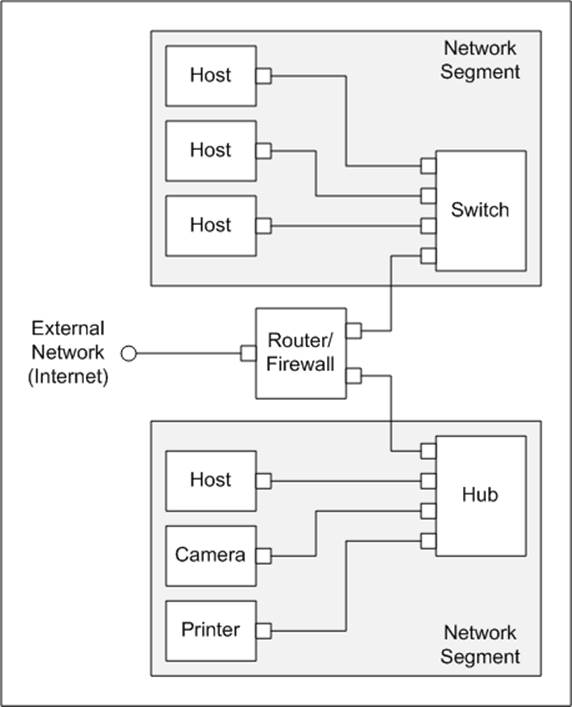
Figure 14-35. An example Ethernet network using a hub and a switch
Ethernet ICs, Modules, and USB Convertors
The microcontroller interface speed is an important factor to take into consideration when you are interfacing to an Ethernet controller IC or module. For an SPI interface, the speed of the serial interface ultimately determines just how fast data can move through the Ethernet IC. For example, a 10 MHz (10BASE-T) IC can theoretically move data at a maximum rate of 10 Mb/s, although in reality it can seldom achieve this because of latencies (slow downs) encountered in the network. A fast SPI interface can transfer data at a maximum rate of 3.4 Mb/s (assuming that the SPI master is capable of this), and that’s much slower than the 10 Mb/s of “slow” Ethernet. Even running full out, the SPI master will never be able to push the Ethernet controller anywhere close to its limit, and I2C is even slower. USB-to-Ethernet ICs and convertors fare somewhat better, since the maximum clock rate of USB V2.0 is 480 Mb/s, but the half-duplex nature of USB can get in the way and again slow things down.
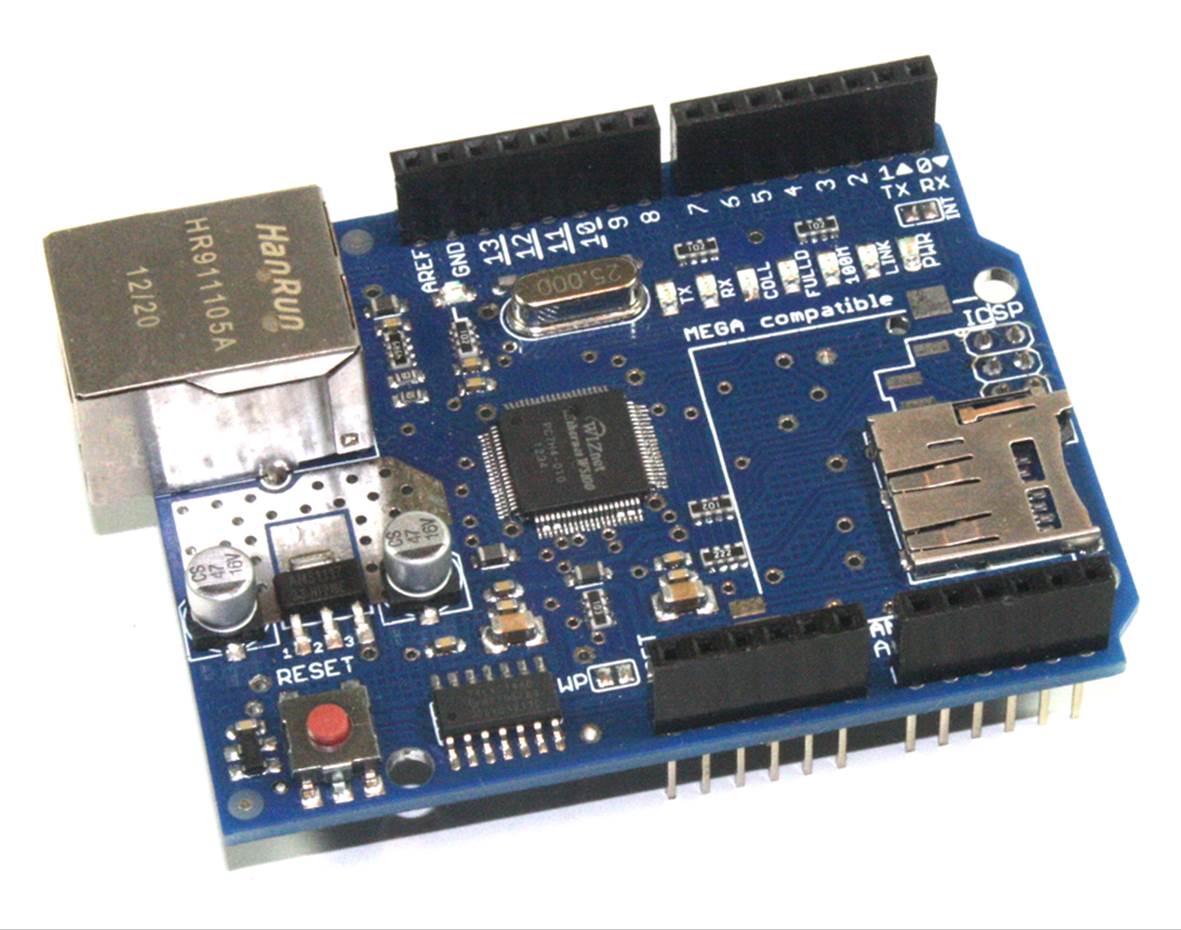
Figure 14-36. Low-cost Ethernet interface module
Many Ethernet ICs use the media independant interface (MII) or reduced media independent interface (RMII) to connect to a microcontroller. This type of interface is designed to provide one part of a network interface and is usually found on 32-bit microcontrollers, such as the ARM Cortex-M3 and Atmel’s 32-bit version of the AVR. MII or RMII allows a fast microcontroller to drive an Ethernet interface IC to near full network speed. For 8-bit microcontrollers, the only real option is an Ethernet controller or module with an SPI interface and slower network data transfer speeds.
For the most part, it’s better to use a prebuilt module than to try to roll your own using just an Ethernet controller IC, but it’s not that hard if you want to make your own PCB. There are a variety of Ethernet component parts to choose from, and Table 14-19 lists a few parts that have been spotted in low-cost modules for microcontroller applications.
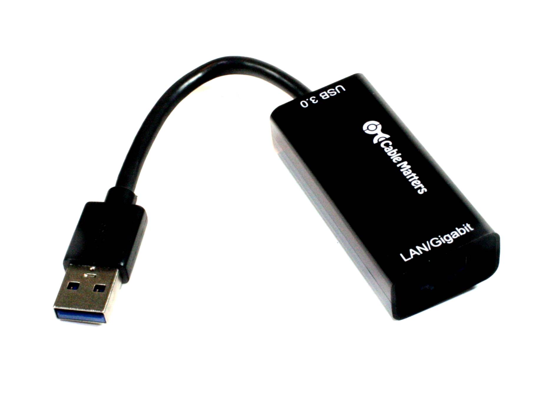
Figure 14-37. USB-to-Ethernet convertor
Figure 14-36 shows one module that uses the W5100. This PCB also has an SD flash card socket, which makes sense, since it is an SPI module and the SD cards use an SPI interface.
|
Part number |
Manufacturer |
Function |
Speed |
Interface |
|
AX88796C |
ASIX |
Ethernet controller |
10/100 |
SPI |
|
KSZ8851SNL |
Micrel |
Ethernet controller |
10/100 |
SPI |
|
LAN9512 |
Microchip |
USB-Ethernet interface |
10/100 |
USB |
|
ENC28J60 |
Microchip |
Ethernet controller |
10 |
SPI |
|
W5100 |
WIZnet |
Ethernet controller |
10/100 |
SPI |
|
Table 14-19. Ethernet ICs |
||||
USB-to-Ethernet convertors, such as the one shown in Figure 14-37, are common and readily available.
These convertors are useful when you want to add a second Ethernet port to a notebook or netbook computer that has only a single Ethernet port (which is most of them). They can also be used with a microcontroller that has a USB host port attached to it. Several companies make USB host port modules like the one shown in Figure 14-38.
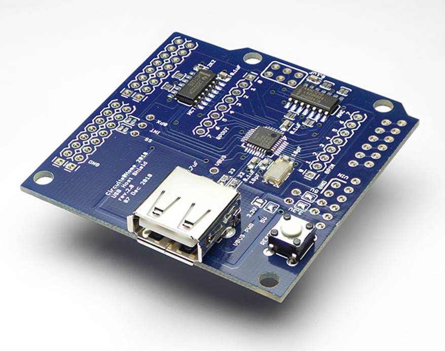
Figure 14-38. Low-cost USB interface module
Wireless Communications
In order to communicate, devices need some way to transfer data. One way is to use wires, but wires tend to get in the way, they can add to the cost of a device or project, and they are a pain to run from device to device. The alternative is to go wireless.
Bandwidth and Modulation
The term bandwidth, as used in this section, refers to the actual range of frequencies employed by a band allocation in the radio spectrum, or by the amount of deviation exhibited by a transmitter at a particular frequency. When tuned to a specific frequency, a transmitter will also radiate some power at frequencies above and below the desired output frequency. Good transmitter design and tuning can eliminate much of this.
A radio carrier by itself doesn’t really carry any information; it is just electromagnetic energy radiated into space at some specific frequency. Early radio systems (and even some in use today) used the technique of interrupting the carrier output to send information encoded in the form of Morse code or some other time-based scheme.
This is just a cursory overview of radio communications and is here mainly to set the stage for the upcoming descriptions of the wireless digital communications components to follow. If you want to learn more about radio technology, I suggest the books Essentials of Short-Range Wireless, The ARRL Handbook, and The Radio Handbook, all of which are listed in Appendix C. You’ll also find a lot of good information available on the websites of wireless component manufacturers.
In amplitude modulation (AM) radio, the level (or amplitude) of the carrier wave is modulated by an input, typically audio. A receiver tuned to the same frequency as the transmitter need only extract the amplitude changes from the carrier to reconstruct the original audio modulation signal. AM is still used for commercial radio, and some early types of remote control and data communications used this technique as well, but it suffers from interference and slow data rates.
Frequency modulation (FM) was developed to overcome the problems of noise and interference experienced with AM radio. With AM, anything from a thunderstorm over the horizon to an automobile with bad sparkplug cables can interfere with the signal, but FM is largely immune to these types of interference. FM works by shifting the frequency of the carrier signal in proportion to the modulation input.
For example, in conventional commercial FM radio, a station operating at, say, 98.4 MHz uses a shift in its carrier frequency that corresponds to an audio input. In the US, FM radio stations are spaced 200 kHz apart, which is more than really necessary but avoids interference between stations. When an audio signal is used to modulate the carrier, it will shift in frequency depending on the polarity of the audio input. The modulation level (how far the carrier frequency will shift) depends on the level of the audio input but is constrained to keep the frequency within the 200 kHz channel. The upshot is that while the frequency of the FM station is nominally 98.4 MHz, the actual frequency at any given moment in time depends on the modulation level.
The modulation technique commonly used for digital communications is called frequency-shift keying (FSK). It is similar to FM except that information is encoded using discrete changes in the carrier frequency. A digital 1 or 0 causes the carrier to shift in frequency by a specific amount. A variation of FSK, called Gaussian frequency-shift keying (GFSK), is used by the GSM mobile phone standard and in the devices described in this section. GFSK works well when you are dealing with binary 0 and 1 values, and the use of GFSK also helps to reduce the overall bandwidth of the signal at a given frequency. This, in turn, helps minimize interference with other devices operating on nearby frequencies.
The ISM Radio Bands
A number of frequency ranges (or bands) have been designated industrial, scientific, and medical use (collectively referred to as the ISM bands). Internationally, these are defined by the ITU-R (International Telecommunication Union-Radio), with individual member countries allowing some or all of these frequencies within their own borders. Table 14-20 lists the ISM bands commonly used for consumer electronic devices in the United States.
|
Lower |
Upper |
Bandwidth |
Center |
|
26.957 MHz |
27.283 MHz |
326 KHz |
27.120 MHz |
|
433.05 Mhz |
434.79 MHz |
1.74 MHz |
433.92 MHz |
|
902.0 MHz |
928.0 MHz |
26 MHz |
915.0 MHz |
|
2.4 GHz |
2.5 GHz |
100 MHz |
2.45 GHz |
|
5.725 GHz |
5.975 GHz |
150 MHz |
5.8 GHz |
|
Table 14-20. Common ISM radio frequency bands |
|||
The 433 MHz and 915 MHz bands are region-specific. The 433 MHz band is assigned to Region 1, which includes Europe, Africa, Russia, the Middle East, and Mongolia. The 915 MHz band is assigned to Region 2 (the Americas). The 27 MHz, 2.45 GHz, and 5.8 GHz bands are worldwide. Other regions, as defined by the ITU, have their own frequency allocations, and some of the ISM bands are subject to local acceptance. The use of these frequencies generally doesn’t require a license, but there are specific types of acceptable uses and the output power of the transmitter is restricted to limit the range and the potential for interference. In the US, this is governed by parts 15 and 18 of the FCC rules. Wikipedia has a good write-up on the ISM bands, including the ones not listed here.
It’s interesting to note that one of the original driving reasons behind the creation of the 2.45 GHz band in the late 1940s was the development of medical diathermy equipment and the microwave oven. The ISM band at 27.120 MHz has been used for CB radio since about 1958, and because CB radios are licensed, the transmitter power they employ in the US is much higher than what would otherwise be allowed under Part 15 rules. Some types of radio-controlled toys still use 27.120 MHz, but they are prone to interference from nearby CB radios. It wasn’t until the 1980s that devices such as cordless phones started to appear on the 915 MHz band, and later on the 2.45 and 5.8 GHz bands, as the necessary semiconductor technology evolved to the point where these applications became economically feasible.
ISM bands with higher frequencies offer better performance in terms of modulation capabilities, but the trade-off is reduced range. The 27 MHz band, for example, doesn’t really have the bandwidth to support FM, but it does support AM and SSB just fine. These modulation methods suffer from external noise (lightning, electrical discharges, and other RF sources) but, on the other hand, it’s not uncommon to hear a CB radio operator many miles away when conditions are right. The higher-frequency bands (915 MHz and above) can support FM and FSK modulation methods because of the increased bandwidth available, and these techniques are relatively immune to many types of interference that plague AM communications. Because of the higher frequencies used and low power output, they don’t have the same range as the lower-frequency bands and are typically limited to line-of-sight or short-range applications.
If you have an application that needs range, but not particularly high data rates, you might want to consider the 433 or 915 MHz bands. If you’re willing to put in the effort to implement an error-tolerant AM protocol (not a trivial project!), then 27 MHz might be an option if you need the range it can offer. This isn’t as crazy as it might sound. If you have access to an old CB radio, or a shortwave receiver with the appropriate band, you can sometimes hear some odd bleeps and blips on the 27 MHz band, along with the usual chatter. Those odd little bits of sound might be anything from a remote-controlled toy to a remote monitoring device reporting to a base station.
There are more ISM band definitions than just those listed in Table 14-20, but for digital data communications, the 433 MHz, 915 MHz, 2.45 GHz, and 5.8 GHz bands are the ones that are most commonly used. Today, the 2.45 GHz ISM band, and to some extent the 5.8 GHz band, are used for things like wireless keyboards, mice, cordless phones, 802.11 (WiFi), Bluetooth, and 802.15 (which includes ZigBee). All these devices compete for the same limited bandwidth. So how do they avoid walking on one another? Well, most of the time the range and frequency seperation is sufficient to minimize collisions, but sometimes it isn’t.
Each ISM band is divided into channels. If you’ve ever configured a wireless router, you’ve no doubt seen a reference to a channel in the configuration menus. In the 2.45 GHz band, the channels used for wireless LAN applications are separated by 5 MHz. Some devices, like the short-range devices discussed in “2.45 GHz Short-Range”, can squeeze even more channels into the 100 MHz bandwidth of the 2.45 GHz band by using narrow-band GFSK modulation. But even if two devices are on the same channel, most wireless devices are able to distinguish between the signals on the basis of signal strength and network addressing in the data packets.
2.45 GHz Short-Range
If you want to define your own communications protocol for a short-range wireless data link, you can do that using a pair of low-cost transceivers operating at 2.45 GHz. A transceiver contains both a transmitter and a receiver. A popular IC component for this type of application is the Nordic Semiconductors nRF23L01+, a single-chip 2.45 GHz transceiver. Modules based on this IC can be purchased for around $2 each. Figure 14-39 shows one example of this type of product.
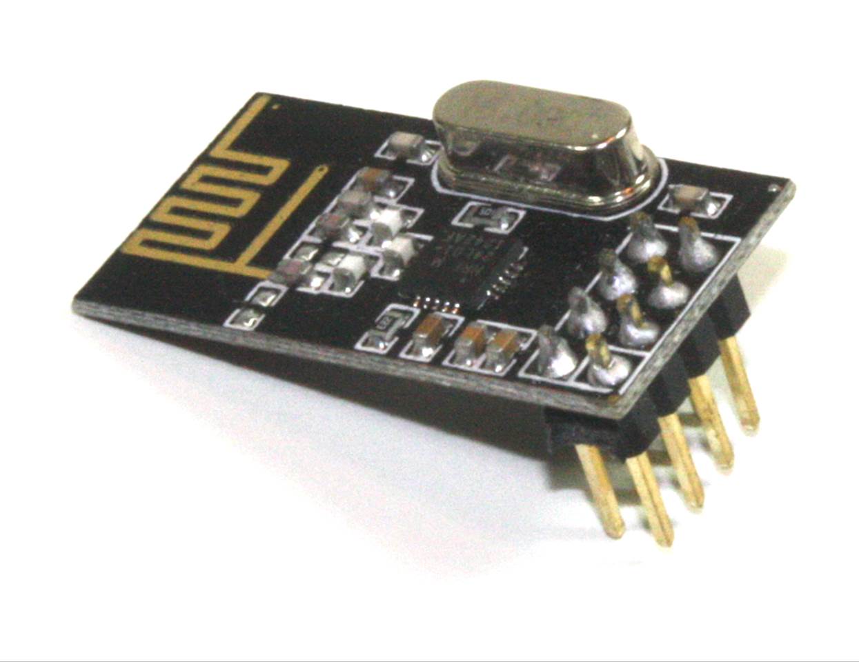
Figure 14-39. 2.45 GHz transceiver module
The nRF23L01+ supports data transmission rates of up to 2 Mb/s in the 2.45 GHz ISM band. This is a half-duplex device, meaning it can be either a transmitter or a receiver, but not both at the same time. It uses an SPI interface to communicate with a host microcontroller, and data is encoded and decoded using GFSK. It supports up to 125 channels within the 2.45 GHz band, and frequency hopping as well. You can download the datasheet for the nRF23L01+ from Nordic Semiconductor’s website.
Note that the nRF23L01+ is just the RF transceiver. It doesn’t impose any type of encoding/decoding scheme on the digital signal. Data to be transmitted is written to the device using the SPI interface, and data received (when in receive mode) is read out. The nRF23L01+ handles the task of asynchronous data reception and decoding internally. Defining the communications protocol and data format is up to the user.
802.11
A wireless local area network (WLAN) based on the 802.11 standard (or WiFi) is much more complex than just a small IC like the one shown in Figure 14-39. 802.11 components also tend to be a lot more expensive.
There are multiple variations on the original 802.11 standard. The b and g standards are the most common, with the 802.11n standard becoming more popular in recent years. The standards differ in terms of the ISM band used and the maximum optimal data rate, as shown in Table 14-21.
|
Standard |
Band (GHz) |
Max data rate (Mb/s) |
|
802.11 |
2.45 |
2 |
|
802.11b |
2.45 |
11 |
|
802.11a |
5.8 |
54 |
|
802.11g |
2.45 |
54 |
|
802.11n |
2.45/5.8 |
600 |
|
Table 14-21. 802.11 standards ISM band and data rate characteristics |
||
Each of the 802.11 standards employs a different type of signal modulation, but you don’t usually need to be too concerned about that. So long as each end of an 802.11 type wireless link can support the appropriate modulation method, they should be able to communicate. This is why it’s common to see an 802.11 device with a designation of 802.11b/g. This indicates that the device will autosense the modulation type and adapt accordingly.
The 802.11 standard (with no letter following it) was originally released in 1997, and by 1999 it had been superceded by 802.11b. Old 802.11 devices are now rare, although some 802.11b devices are still in use. 802.11g (2003) and, more recently, 802.11n (2009) have become the most commonly used standards of the 802.11 family.
Two new variants, 802.11ac and 802.11ad, have only recently been formalized, and devices capable of using these new standards are still in development. 802.11ac uses the 5.8 GHz band but supports data rates up to 6.9 Gb/s. 802.11ad is unique in that it operates on a 60 GHz band with a projected data rate of upward of 6.7 Gb/s.
As with wired Ethernet (described in “Ethernet Network Communications”), you might want to avoid the complexity of dealing with the low-level details of the interface and use something that will do the heavy lifting for you, such as the module shown in Figure 14-40. This particular part sells for about $85 USD from DFRobot (see Appendix D for its website URL).
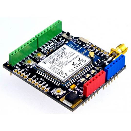
Figure 14-40. 802.11 b/g transceiver module (courtesy of DFRobot)
The part of the unit that does the actual work is the rectangular module with the metal cover sitting in the middle of the PCB, in this case a WizFi210 from WIZnet. One of the things that makes this and other WiFi modules pricey (relatively speaking) is that chip manufacturers such as WIZnet have already gone through the process of certifying the operation of the module and obtaining an FCC ID number, which implies that it has been tested and verified to comply with FCC regulations. This is not an inexpensive undertaking, so purchasing a module that is already compliant and certified makes good sense.
A WiFi module intended for embedded applications, the Microchip MRF24WB0MA, is available for around $30 USD from distributors such as Digikey and Mouser (see Appendix D). It uses an SPI interface and is available already mounted on a PCB. Another possibility is the CC3000 802.11 b/g module from Texas Instruments, which is a popular part found in many low-cost WiFi modules. An evaluation board with the CC3000 installed (TI part number CC3000EM, available from Mouser and other distributors) runs about $38 USD, and bare modules (no supporting PCB) based on the CC3000 sell for between $17 to $28 USD in small quantities. The evaluation board is not much different from boards made for devices like the Arduino and BeagleBone, there’s no need to do surface-mount soldering, and it’s not that much more expensive, so it might be worth considering.
Although there are multiple WiFi transceiver components available, it is a good idea to find one already mounted on a PCB with the appropriate antenna connector and associated circuitry. Laying a out a PCB for RF can be tricky, and it’s something of a specialized activity. You can save yourself a lot of effort and aggravation by buying a product where someone else has already worked out the kinks for you.
Table 14-22 lists the 802.11 modules mentioned in this section. The datasheets available for these parts describe the operation and provide reference designs if you really want to build your own PCB. If you do take this path, be sure to follow the manufacturer’s recommendations for PCB layout.
|
Part number |
Manufacturer |
Internal controller |
Interface |
|
MRF24WB0MA |
Microchip |
Proprietary |
SPI |
|
SPWF01SA |
STMicroelectronics |
ARM Cortex-M3 |
SPI, I2C, UART |
|
CC3000 |
Texas Instruments |
Proprietary |
SPI |
|
WizFi210 |
WIZnet |
Proprietary |
SPI, I2C, UART |
|
Table 14-22. 802.11 b/g modules |
|||
All of these modules are complete plug-in 802.11 b/g functional blocks. All that’s needed is a microcontroller or microprocessor (available through Allied, Digikey, Mouser, Newark, and other electronics distributors) to provide data and control.
Bluetooth®
This section discusses what is sometimes called Classic Bluetooth. With the release of version 4 of the specification from the Bluetooth SIG, a new specification came into being, called Bluetooth Low Energy, Bluetooth Smart, or Bluetooth LE. The new technology is a low-power, reduced-complexity protocol that is not backward compatible with Classic Bluetooth. “Bluetooth Low Energy (BLE)” discusses Bluetooth Low Energy.
Bluetooth is a wireless technology standard designed for data exchange data over short distances. Bluetooth operates in the 2.45 GHz ISM band (see “The ISM Radio Bands”). It was invented in 1994 by the telecommunications company Ericsson, which originally envisioned it as an alternative to the then-prevalent RS-232 cables used to connect various devices such as PCs, PDAs (personal data assistants, like Palm Pilots), and printers. The Bluetooth trademark is protected by the Bluetooth Special Interest Group (SIG), and in order for a product to be called a Bluetooth device, it must be qualified to standards defined by the SIG.
Two key characteristics differentiate Bluetooth from other technologies operating in the 2.45 GHz band. The first is the protocol that it employs, which allows for the creation of ad hoc networks of devices with secure connections (pairing and bonding). The second is its ability to utilize a frequency-hopping spread-spectrum technique to improve communications reliability.
The frequency-hopping spread spectrum technique employed by Bluetooth involves dividing the transmitted data into packets, each of which is transmitted on one of 79 channels. Each channel has a bandwidth of 1 MHz. The newer 4.0 standard employs channels with a bandwidth of 2 MHz, which reduces the number of available channels to 40. Up to about 1,600 channel hops are performed per second, depending on the selected mode of operation.
To associate one device with another, Bluetooth uses a process called bonding. A bond is created as the result of a process known as pairing. When a bond is established between two Bluetooth devices, a special code called a link key is held by both devices and known to only those two devices. Once devices have been bonded, they can authenticate each other whenever they are in range, so the user doesn’t need to repeat the process each time a link needs to be established.
Bluetooth employs a master/slave communications protocol, but there are no dedicated roles among devices. A master device can communicate with up to seven other Bluetooth devices in an ad hoc Bluetooth network. Any device can, by agreement with other devices, become the master until another device needs to take on that role and initiate a data exchange transaction.
Bluetooth devices are divided into three classes, each of which defines a maximum transmit power and a maximum operating range under optimal conditions, as shown in Table 14-23.
|
Class |
Max power |
Operating range |
|
Class 1 |
100 mW |
100 meters |
|
Class 2 |
2.5 mW |
10 meters |
|
Class 3 |
1 mW |
1 meter |
|
Table 14-23. Bluetooth classes |
||
The effective range of any link is limited by the device with the least range. A Class 2 device will work fine with a Class 1 device, but the resulting link between bonded devices will never be better than Class 2. Also be aware that, even though the range for a Class 1 device is given as 100 meters, in reality it can be much less, depending on the local environment.
The data rate of a Bluetooth device is defined by the revision level of the specification. Table 14-24 lists the defined data rates. In practice, the actual data rates will typically be lower due to processing overhead and other factors.
|
Version |
Data rate |
|
1.2 |
1 Mb/s |
|
2.0 + EDR |
3 Mb/s |
|
3.0 + HS |
24 Mb/s |
|
4.0 |
24 Mb/s |
|
Table 14-24. Bluetooth data rates |
|
The best and least expensive way to put Bluetooth to work is to purchase a module. There are many to choose from, ranging in price from about $9 up to around $60 USD, depending on the data transfer speed and range capability. Table 14-25 lists some readily available modules that can easily be incorporated directly into a circuit. This list is by no means complete, so be sure to look around for a module that suits your needs (and your budget).
|
Part number |
Manufacturer |
Interface |
|
Class |
PAN1315A |
Panasonic |
|
UART |
1 and 2 |
RN41 |
|
Microchip |
UART/USB |
1 |
|
RN42 |
Microchip |
UART/USB |
|
2 |
RN52 |
Microchip |
|
UART/USB |
3 |
SPBT2632C1A |
|
STMicrotechnology |
UART |
3 |
|
WT11i |
Bluegiga |
UART/USB |
|
1 |
WT12 |
Bluegiga |
|
Table 14-25. Bluetooth modules |
||
Most Bluetooth modules come with the protocol already built in. This greatly simplifies things, since in most cases using a module just involves connecting it to your circuit. Once it’s connected, you can then pair it with another Bluetooth device and start transferring data.
The Bluetooth wordmark and logos are registered trademarks owned by Bluetooth SIG, Inc. For more information about Bluetooth, see the SIG website.
Bluetooth Low Energy (BLE)
Bluetooth Low Energy (BLE) is a low-power alternative to the previous versions of the Bluetooth specifications, now often referred to as Classic Bluetooth. Marketed as Bluetooth Smart, BLE is a wireless personal area network (PAN) technology defined by the Bluetooth SIG and intended for applications in healthcare, fitness, home entertainment, and security, among others.
The original Bluetooth specification was not specifically created with PAN applications in mind, but rather as a replacement for serial and parallel interface cables between a host computer and various peripheral devices. Consequently power requirements were not a major design consideration. This puts Classic Bluetooth at a significant disadvantage in ultra-low-power applications. Although Bluetooth has been incorported into things like mice and keyboards, these products suffer from short battery life compared to other types of low-power wireless technologies. BLE is intended to provide significantly reduced power consumption and component part cost while still operating at a similar range and with enhanced data-transfer capability.
Version 3 Classic Bluetooth utilizes a synchronous protocol that is basically always on, by virtue of the periodic synchronization data exchanges that occur every 600 microseconds to maintain a communications link. Consequently, even an idle device continuously uses power. In addition, when a link between devices is broken, it can take upward of a second to reestablish the connection. This is too long for some PAN applications.
Like Classic Bluetooth, Bluetooth Low Energy uses a synchronous protocol but with a synchronization interval that can be varied dynamically from 5 ms up to several seconds. To conserve on energy expended to transmit data, a BLE packet can squeeze in more data than with a Classic Bluetooth packet, and the packet length is variable to accommodate different situations.
These features, combined with other power-saving techniques such as reduced transmit power, enhanced receiver sensitivity, maximized standby time, and reduced packet complexity, result in less power expended per bit. In other words, BLE can provide higher average data throughput rates while expending less energy to do it.
Bluetooth Low Energy uses a unique protocol and a simpler modulation scheme, and it is not backward compatible with the previous Bluetooth Classic protocol. However, the Bluetooth 4.0 specification permits devices to implement either the BLE or Classic protocols, or both, in a single device, and many transceiver chips now available can operate in dual mode. BLE operates in the same 2.4 GHz radio frequency band as Classic Bluetooth but utilizes a different set of channels. This allows dual-mode devices to share a single radio antenna.
In some applications, a BLE transceiver can operate for extended periods of time (on the order of months, or possibly even years) on a single coin cell battery such as a CR2032 (see Chapter 5). Many modern mobile and desktop operating systems such as iOS, Android, OS X, and Windows 8 provide native support for BLE. Other platforms are possible with the appropriate low-level software and transceiver hardware.
Transceiver chips for BLE are available from many of the same sources as Classic Bluetooth transceivers. Table 14-26 lists some of the IC components available.
|
Part number |
Source |
Interface |
|
MCU/Controller |
CC2541 |
Texas Instruments |
|
I2C |
8051-based |
CSR1010 |
|
CSR |
UART/SPI |
Proprietary |
|
EM9301 |
EM Microelectronics |
UART/SPI |
|
Proprietary |
nRF8001 |
Nordic Semiconductor |
|
Table 14-26. Bluetooth LE ICs |
||
While there don’t seem to be as many modules for BLE as for Classic, there are products available from several sources, such as the ones listed in Table 14-27.
|
Part number |
Manufacturer |
Interface |
|
ABBTM-NVC-MDCS71 |
Abracon |
UART/I2C/SPI |
|
BLE112 |
BlueGiga |
UART/USB |
|
PAN1720 |
Panasonic |
UART/SPI |
|
Table 14-27. Bluetooth LE modules |
||
If you don’t want to go the do-it-yourself route, the SensorTag device from Texas Instruments is popular with folks using an iPad, iPhone, or Andoid device. It costs about $25 USD and includes a range of sensor input types, including temperature, humidity, pressure, accelerometer, gyroscope, and a magnetometer.
Adafruit sells a module for BLE, called the Bluefruit LE. This essentially an nRF8001 breakout that uses an SPI interface (which is what the nRF8001 uses) to communicate with something like an Arduino. Figure 14-41 shows what the board looks like. Adafruit provides a free, open source app to communicate with the Bluefruit, and there is a demo video on the Adafruit website.
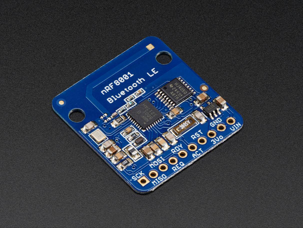
Figure 14-41. Bluefruit LE breakout module from Adafruit
Zigbee
ZigBee is a wireless technology standard used to create short-range data communications links and ad hoc networks for applications that only require a low data rate, long battery life, and secure communication. The ZigBee specification is based on the IEEE standard 802.15.4 for low-rate wireless personal area networks (WPANs). The ZigBee specification adds a network layer and an application layer (along with other functions). For additional information about ZigBee and the ZigBee standard, visit the ZigBee Alliance.
ZigBee devices can be used to create mesh networks, wherein multiple low-power, short-range devices cooperate to move data between intermediate devices. This allows widely separated ZigBee nodes to communicate over distances beyond the normal range of each individual device. Security is an integral part of the specification and is implemented through predefined shared encryption keys.
As with the other wireless technologies covered in this chapter, ZigBee operates in the ISM radio bands (see “The ISM Radio Bands”). In the US, it can use either the 915 MHz or the 2.45 GHz bands, although most commercially available ZigBee devices and modules use the 2.45 GHz band. In Europe, ZigBee devices operate on either the 868 MHz or the 2.45 GHz bands.
The data rate for a ZigBee link depends on the ISM band it is using, as shown in Table 14-28. A maximum data rate of 250 Kb/s isn’t particularly fast, but for the monitoring and control applications that are the primary applications for ZigBee, it’s usually more than fast enough.
|
ISM band |
Data rate |
|
868 Mhz |
20 kb/s |
|
915 MHz |
40 kb/s |
|
2.45 GHz |
250 kb/s |
|
Table 14-28. ZigBee data transfer rates by ISM band |
|
The technology defined by the ZigBee specification is intended to be simpler and less expensive than other technologies, and in general terms, this is true. But it is also true that some Bluetooth RF modules are about the same price as a 2.45 GHz ZigBee module; so in the end, it really comes down to what you want to do and which technology best suits your needs.
Possible applications for ZigBee include wireless lighting and appliance control, distributed data acquisition, electrical service meters, robots, and traffic control systems. ZigBee RF modules with minimal interface and programming requirements are readily available (see Table 14-29).
|
Part number |
Manufacturer |
ISM band |
Interface |
|
ATZB-24-B0R |
Atmel |
2.45 GHz |
I2C, SPI, UART |
|
XB24-AWI-001 |
Digi International |
2.45 GHz |
UART |
|
MRF24J40 |
Microchip |
2.45 GHz |
SPI |
|
CC2420 |
Texas Instruments |
2.45 GHz |
SPI |
|
CC1120 |
Texas Instruments |
868/915 MHz |
SPI |
|
Table 14-29. ZigBee modules |
|||
When considering a ZigBee RF module, be sure to look for features like built-in protocol logic. This will greatly simplify things, because it makes the interface to the module a simple read or write data transaction, and there’s no need to install software to deal with the ZigBee network and application layers.
Other Data Communications Methods
In addition to wires and radio waves, data can be carried over a light beam (a laser) and through the AC wiring in a home or office. The remote controls used with television and stereo receivers (and just about everything else in the home entertainment section of the department store) use pulses of infrared light to send commands to various devices. Infrared has also been used to send documents to a printer from a handheld personal organizer, and some tablets include the ability to send commands or data using an infrared LED built into the tablet’s case.
As with the short-range 2.45 GHz transceivers described in “2.45 GHz Short-Range”, you can devise your own communications protocol for an optical system. All you really need is an IR LED like the one shown in Figure 14-42 and a phototransistor receiver, like the module shown inFigure 14-43. You will also need a lens of some sort to help focus the light if you want to extend the range beyond just a few feet. A toy telescope or binoculars work well for this purpose.
Figure 14-42. Infrared LED module
If you think about the IR link as a type of wire, you can see that it would be easy to send an RS-232 type signal over the link. A second link, from the remote device back to the base location, would complete the TxD/RxD loop, and presto, you would have a link that could theoretically work over long distances—assuming, of course, that the light source is powerful enough and the weather is clear. Systems like this have been implemented via solid-state IR lasers, and some people have used modified red and green laser pointers for this purpose.
If you decide to work with lasers, be careful about where they are pointed. Setting up a visible laser link between two points at high elevations is not a good idea. If an aircraft flies through the beams, it can be bad news for you legally, and it can endanger the aircraft if the pilots are momentarily blinded by the laser reflections off the cockpit windows. A non-coherent (nonlaser) narrow-beam link is safer, but it will require some decent optics at each end and some serious tweaking to get it to work reliably. If you just want to set up a laser link between one structure and another a couple hundred meters away, then you’re probably good to go—assuming it doesn’t start to rain or blow dust in the middle of a big download, of course.
Figure 14-43. Infrared receiver module
Summary
The communications protocols covered here range from the straightforward simplicity of SPI, I2C, RS-232, and RS-485, to the complexity of USB and Ethernet. Fortunately, IC components and modules are available that hide much of that complexity and present an SPI or I2C interface. We also covered some of the complexity of 803.11 wireless networks, took a quick look at the underlying machinery of USB, and reviewed Bluetooth and ZigBee wireless technologies and some of the components available to implement them.
This chapter has covered a lot of ground and touched on a number of technologies, but the key theme is how the data is physically transferred. It might involve wires, radio waves, or light beams, but it all comes down to serial data communication using either synchronous or asynchronous methods. From what has been presented here, you should be able to make some good initial decisions about the type of data communication method is best suited for your application.
For wireless communications, a generic 2.45 GHz link is fine for short-range communication where security is not a major concern and you don’t need to support a network architecture. If a secure short-range link is needed for intermittent data transfers, ZigBee would be a possible candidate.
Moving up in speed, Bluetooth offers both secure communications and fast data exchange rates of up to 24 Mb/s. For even faster data rates, with full networking capability, consider one of the 802.11 standards.
Outlining the communication technologies we’ve covered here, Table 14-30 is one way to organize a decision list based on communication speed.
|
Connection |
Speed |
Data link type(s) |
|
Wireless |
Low |
2.45 generic, ZigBee |
|
Wireless |
High |
802.11b/g/n, Bluetooth, Bluetooth LE |
|
Wired |
Low |
RS-232 |
|
Wired |
High |
Ethernet, RS-485, USB |
|
Table 14-30. Communication types organized by speed |
||
Ultimately, your decision comes down to how much you’re willing to spend, how much work you are willing to do to make a functional communications link, and how secure you need that link to be. Be sure to explore the resources available from the various manufacturers, distributors, and PCB module suppliers. Also, don’t forget to check out the books listed in Appendix C for low-level, hands-on details.
All materials on the site are licensed Creative Commons Attribution-Sharealike 3.0 Unported CC BY-SA 3.0 & GNU Free Documentation License (GFDL)
If you are the copyright holder of any material contained on our site and intend to remove it, please contact our site administrator for approval.
© 2016-2026 All site design rights belong to S.Y.A.