Practical Electronics: Components and Techniques (2015)
Chapter 15. Printed Circuit Boards
This chapter presents an overview of printed circuit board (PCB) design and layout, with a focus on technique rather than specific tools. Special attention is given to topics such as PCB material, multilayer techniques, and surface-mounted components.
PCB History
Prior to the invention of printed circuit boards, assembling an electrical or electronic device was an arduous process. Insulated posts or metal tabs riveted to insulating strips provided the connection points for the various components, and insulated wires (most of the time) routed signals and voltages from one part of the circuit to another. All of it was assembled by hand. Figure 15-1 shows an example of the level of effort involved, with an image of the Atwater-Kent radio assembly line from some time in the early 20th century.
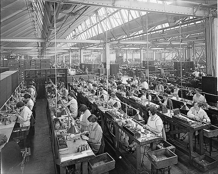
Figure 15-1. A vacuum tube radio assembly line at the Atwater-Kent factory circa 1925 (photograph from Library of Congress)
Starting in the late 1950s, the point-to-point wiring of electronic devices was gradually replaced by simple single- or double-sided printed circuit boards, as shown in Figure 15-2. The vacuum tubes are still there, but instead of wires running all over and resistors and capacitors suspended between terminal strips and solder posts, they are now mounted on a PCB. A circuit like this (which happens to be a plug-in module from a Hewlett-Packard 140A oscilloscope) was still largely assembled by hand, but the process typically had fewer wiring defects and resulted in overall higher quality.
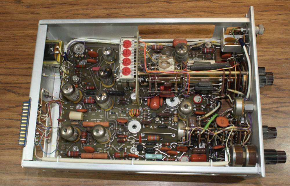
Figure 15-2. A plug-in module from a vacuum tube oscilloscope, circa 1963
With the widespread adoption of solid-state components, and later integrated circuits, the size of circuits shrank and is still shrinking today. A multi-layer PCB with both through-hole and surface-mount components is similar to the Texas Instruments MSP430 development board shown inFigure 15-3.
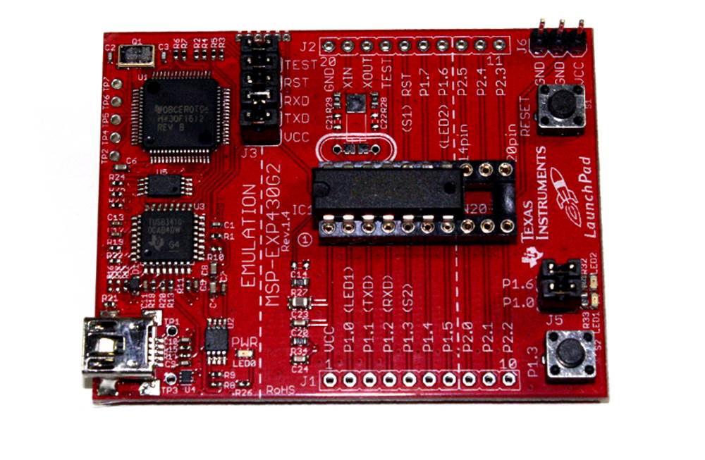
Figure 15-3. MSP430 microcontroller development board
It’s tiny, but if it were built with 1980s technology, it would probably be two or even three times larger. Today, robots called pick-and-place machines grab surface-mount parts from a strip wound on a reel, place them on the board in the correct orientation at the correct location, and then go back and repeat the process for each surface-mounted part on the PCB. Some of these machines move incredibly fast, and they can populate a PCB with parts in a matter of a few minutes.
A look at the motherboard inside a modern PC will serve as an example of just how far PCB technology has progressed in the past 50 years. Today, many commercially produced PCBs cannot be assembled by hand, even if you wanted to. They are just too dense, and the parts are too small. Without automated PCB fabrication machines to make the base circuit boards, robots to place the parts on the PCB, and still more automation to solder and test the finished PCB, many of the electronic devices we have today could not exist.
But there is still a lot you can do with a simple PCB and the soldering techniques described in Chapter 4. This chapter takes a high-level look at how to go about designing and fabricating a PCB without ordering thousands at a time.
PCB Basics
A printed circuit board is built on a sheet of insulating material, called the substrate. Some types of PCBs have a layer of copper laminated to one or both sides. Unwanted copper is etched or routed away, leaving the circuit traces (the wiring) and the component mounting locations (pads). Other types start with a bare substrate board and add the copper to it to create the circuits on the board. Figure 15-4 shows what goes into a blank copper-clad, double-sided PCB.
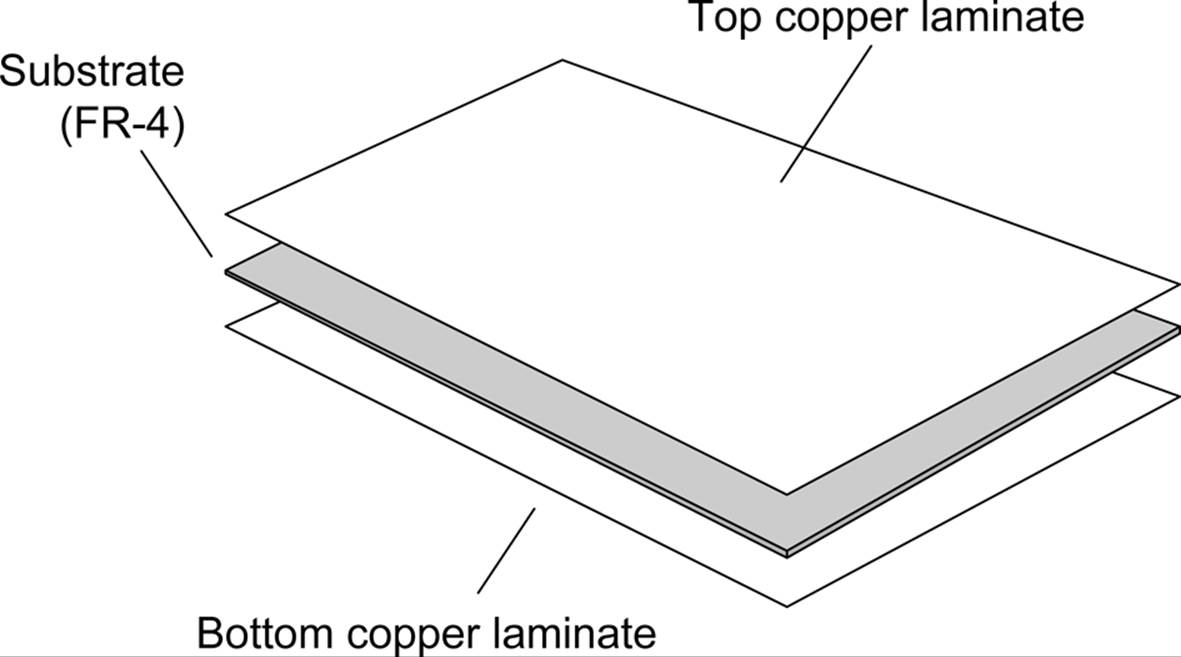
Figure 15-4. Basic double-sided blank PCB
Multi-layer PCBs are fabricated from stacks of thin substrate sheets, each with a copper circuit pattern on one side. After the circuit has been created on the substrate sheets, they are stacked and bonded to create a single PCB. A multi-layer PCB can have upward of 10 internal layers. A special type of pad, called a via, is used to connect traces between sides and layers, so that a circuit that begins on the top (component) side of the multi-layer stack might connect to a trace on the third layer, which in turn might connect to a trace on the solder (back) side of the PCB.
The substrate material is usually either a phenolic material (XXXP/FR-2) or a resin-impregnated woven fiberglass sheet (FR-4). The FR value indicates the flame resistance grade of the material.
Pads, Vias, and Traces
A PCB layout consists of three basic types of shapes: pads, vias, and traces. Pads are where components are mounted to the PCB, which for through-hole parts (for example, a 1/8W resistor) will consist of a hole for a lead surrounded by an annular ring of copper. A via is typically smaller than a pad and, as noted earlier, is used to route a signal or power from one layer of a PCB to another (front to back for instance, or perhaps to an internal layer in a multi-layer board).
In double-sided or multi-layer boards, through-hole pads and vias are usually plated to create a thin tube of copper between the endpoints of the hole. For some homemade PCBs, this isn’t possible (at least not easily), so a piece of bare wire can be soldered into the via on both sides. Through-hole components should also be soldered on both sides if there is no plating in the lead hole of the pad and there are traces on both sides.
Traces are the wiring of the circuit. Trace width determines the amount of current that can be safely passed through the trace without causing potentially damaging resistive heating. The thickness of the copper laminate also has an effect on the current carrying capacity.
Surface-Mount Components
Surface-mount technology (SMT) devices are soldered directly to one side of a PCB (it is possible to have SMT parts on both sides of a PCB). There are no holes for the leads of SMT parts, just solid pads for the leads to attach to. Usually, solder paste is used (rather than regular stick solder) to make the connection, and the solder paste is melted through a process such as reflow soldering, infrared heating, or just a plain fine-tip soldering iron.
Fabrication
PCB fabrication processing can take one of two forms: subtractive or additive. The subtractive process is the one most commonly used for small production runs, and it involves using an acid to remove unwanted copper from a PCB, leaving just the traces and the component connection pads. The additive process can take the form of full additive, starting with a bare substrate and building up the copper circuit pattern using a plating technique. A variation on this is the semi-additive process, where a substrate has a thin layer of copper applied, the unwanted portions are removed, and the final desired thickness is built up on the existing thin layer of traces and pads. Multi-layer PCBs are usually produced through the semi-additive process, because the plating used inside the connections between circuit boards (the vias) can be applied as part of the production process.
For an etching process (subtractive) the steps basically follow those shown in Figure 15-5. These are the same basic steps you would follow if etching a PCB in your own workshop, but the PCB fabrication houses have equipment to make the whole process a lot more precise and efficient.
After the board is etched, the various holes are drilled. Then pads and vias are plated to make a connection with both sides of the PCB (if it’s a double-sided board, of course). The bare copper might also receive a thin plating of tin to make soldering easier. Finally, a commercial PCB fabricator can apply a solder mask to prevent the solder in a wave-solder machine from sticking to places where it shouldn’t, and a silkscreen mask is applied to one or both sides. The silkscreen mask typically has component outlines, part numbers, and the name of the company or individual who designed the PCB.
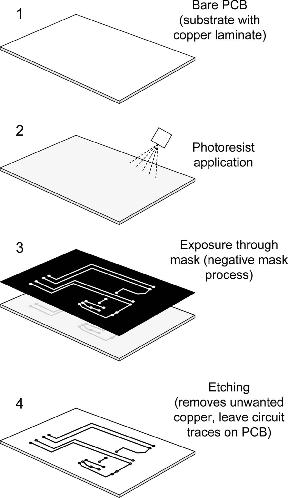
Figure 15-5. Basic steps for subtractive etching
Refer back to Figure 15-3. The material covering the board (it’s red) is the solder mask. Over that is the silkscreen with some information about the board and a logo. The underlying traces are barely visible through the solder mask.
PCB Layout
PCB layout is the process of arranging components on a PCB within a given area and then deciding where to place (or route) the traces to connect them into a complete circuit. It is something of an art, and it’s not uncommon to try multiple times until the component placement and trace routing work without conflicts or spacing that is too narrow. It is also not uncommon for a PCB layout to look nothing at all like the original schematic. Physically, it doesn’t matter (generally) where components are placed, particularly with small PCBs. So you might find R1 at the lefthand side of a PCB, and R2 way over in the lower-right corner. So long as they are connected correctly, it doesn’t really matter; what matters is that they are placed to take advantage of the available space on the board.
In the past, PCB layout was done using a sheet of clear plastic film to create the layout pattern with adhesive black press-on tape, pads, and vias. This was usually done at 4X size, and then scaled down with a special camera to create the final mask. The trace tapes came in difference widths, and pad shapes were available in 1X, 2X, 4X, and even 8X sizes. The designer could spend many days at a light table carefully applying the tape and picking up the individual pads and vias and placing them with the point of a razor knife. A photographically created grid on a transparent sheet was placed under the clear working sheet to provide placement reference. As you might suspect, the whole process was rather tedious. It also explains why old PCBs tend to have occasional wavy trace lines, rounded trace curves, and irregular trace spacing. Each one was done by hand.
Although it is possible to create a simple PCB layout on a clear piece of plastic with adhesive tapes and pad transfers or a special pen, it’s easier to use a software tool made for that particular purpose. Some PCB kits employ a laser printer to transfer the layout pattern, while large PCB fabrication houses might use a photo plotter to create the positive or negative photo-resist exposure mask. A photo plotter uses a special head with a variable aperture that exposes an underlying photosensitive film as the plotter head moves across it. After exposure, the film is developed and the transfer mask is ready to use.
The following steps show one way to lay out a PCB using a tool like the PCB layout editor that is provided as part of the gEDA package. The layout editor can also be obtained as a standalone tool, and other software packages are available that also have PCB layout editors (Eagle, FreePCB, KiCad, and others). Refer to Appendix D for resource information and URL links. In general, however, the steps are basically the same for any PCB layout tool, or even if you are doing the layout the hard way with press-on tape and die-cut pads.
Determine Dimensions
First, decide on the dimensions of your PCB. If you have the parts available that will be used on the PCB, you can arrange them on a piece of graph paper to see how they will fit. Some CAE tools also provide package placement drawings as part of their component library, so you can model the topography of a PCB using the package outlines supplied with the CAE tool (see “Place Components”).
To avoid situations where the lead of a component is blocked by another part, make sure to leave sufficient space for both parts and traces. If you are designing a single-side board, this is particularly important, and you might need to account for jumpers to route signals and voltages over one or more traces. For a double-sided board, leave enough room to place a via to take the trace to the other side of the PCB if you need to route under or around other parts.
Arrange Parts
Second, decide where the mounting holes and pads for things like terminal blocks, I/O connectors, and wires will go. This establishes the physical mounting and interface geometry for your PCB. Figure 15-6 shows what a layout looks like after this step is complete.
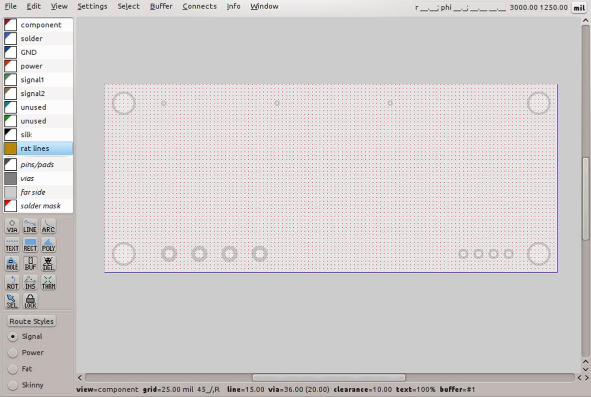
Figure 15-6. PCB dimensions, mounting holes, and interface pad locations
When placing I/O and power connector pads, you will need to reference the placement from the edge of the PCB. Say, for example, you want to have a row of pin sockets with 0.1-inch spacing, like the ones found on Arduino, BeagleBoard, or MSP430 boards (see Figure 15-3). How close should the part be placed to the edge of the board? Generally, for something like this, it is a good idea to leave at least 0.15 inch to 0.2 inch of space between the pins and the PCB edge, as shown in Figure 15-7. It is generally not a good idea to route a trace between the row of connector pins and the edge of the board. It’s just too easy for the trace to be damaged, and it precludes any trimming that might be needed to make the board fit in a tight location.
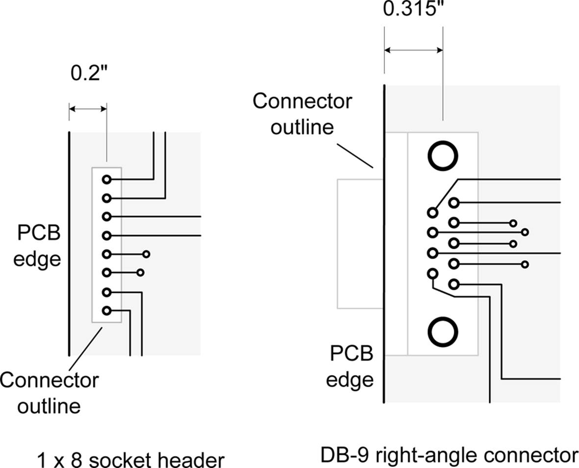
Figure 15-7. PCB connector placement
For things like right-angle DB connectors (DB-9, DB-25, etc.), the physical shape of the connector determines where it will be placed. The component library of a well-stocked PCB layout editor will have the general dimensions for common parts, but they should be checked, as each manufacturer can do things a bit differently. Figure 15-7 shows a DB-9 connector with a board edge-to-connector mounting-hole dimension of 0.315 inch. This number is obtained from the manufacturer’s data sheet for the part.
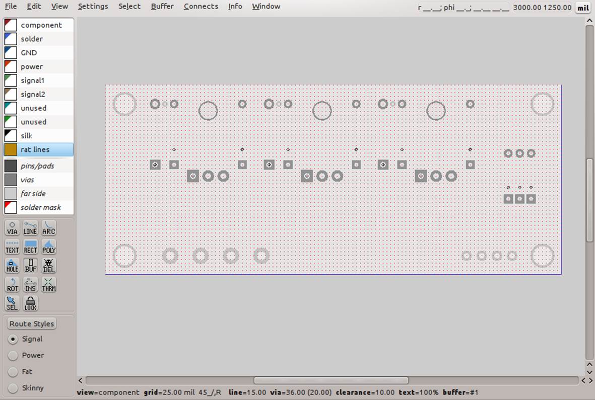
Figure 15-8. Component placement
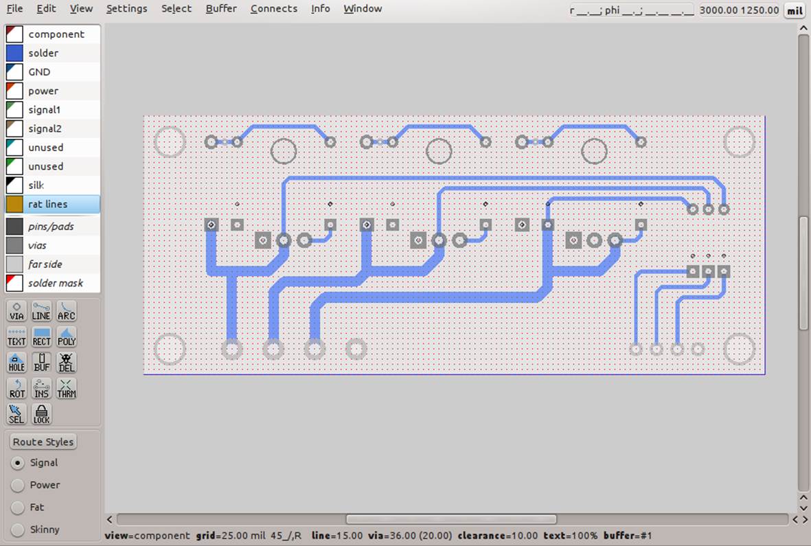
Figure 15-9. Solder-side traces
Place Components
Next comes component placement, which is shown in Figure 15-8. Here we have three silicon-controlled rectifier (SCR) devices and some Zener diodes, resistors, and capacitors. They are connected to the PCB with wires soldered though pads along one edge, as defined in “Arrange Parts”.
As with the connectors discussed in “Arrange Parts”, the footprint of each part is obtained from a library of component shapes that comes with the PCB layout tool. Select a part from the library and place it on the PCB layout area. You can easily move parts around before the traces are placed, so now is the time to get the best layout geometry for the available board space.
Route Traces on the Solder Side
Now comes the fun part: routing the traces. If you have a complex design, this is where you might want to turn it over to an auto-router and let it have a go at figuring out where to place the traces. The downside is that even the best auto-routers sometimes don’t get it right, in which case you will have to go back in and rip up some, or all, of the auto-router’s work and do it yourself. On the plus side, an auto-router will generally apply best practices and avoid some of the common mistakes that humans are prone to making.
This is a double-sided board, so we start with the solder (or back) side first. Figure 15-9 shows the traces for the solder side of the PCB. Note that some of them are rather hefty. These traces will carry a lot of current, so making them wider is equivalent to using a heavier gauge of wire.
Route Traces on the Component Side
Next comes the component (or top) side of the PCB. Here, you want to make sure not to create trace collisions or come too close to component pads. It’s OK to go under a component like a resistor, so long as there is sufficient space between the traces and the component’s pads. When working with DIP IC packages, you can also run a thin trace between the pads for the IC’s leads. The leads of most surface-mount ICs are too closely spaced for this, so the typical solution is to route some of the device’s leads to vias under the chip package and pass them through to the other side. This PCB layout doesn’t need to do that, however. Figure 15-10 show the traces on the component side of the PCB.
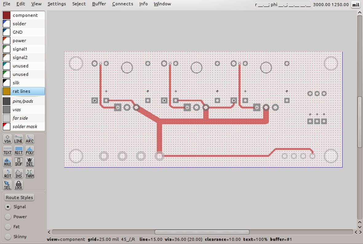
Figure 15-10. Component-side traces
Create the Silkscreen
The last layout step is to create the silkscreen for the PCB. This is an optional step that results in the fabrication house creating a silkscreen and literally painting the component outlines, part numbers, and other information directly on the finished PCB. Figure 15-11 shows the PCB with both the top and bottom layers and the silkscreen visible. The layout tool created the part outlines for us using the component data in its library. The additional lettering is supplied by the layout designer.
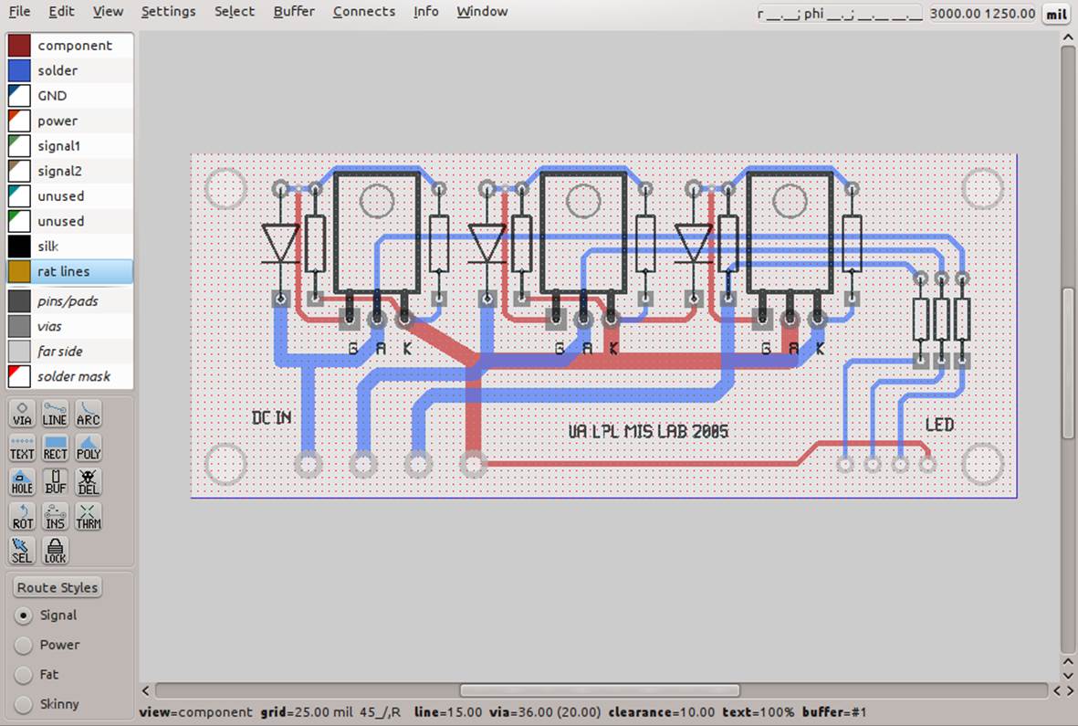
Figure 15-11. Silkscreen view
Generate Gerber Files
After finishing the layout, save it to disk and then create a set of files that can be used to fabricate it. That’s assuming, of course, that you have wisely elected to use a fabrication service (see “Fabricating a PCB” for some thoughts on this).
The industry standard way of doing this is by means of so-called Gerber files, named after the company that developed automated photo-plotting equipment early in the history of PCBs. Each PCB layout consists of multiple Gerber files. These define the top pattern, the bottom pattern, any intermediate layers (for multi-layer boards), solder masks, a solder paste mask (for surface-mount components), top and bottom silkscreen templates, and a drill list that defines the sizes of the holes, how many of each, and where they are to be drilled. Figure 15-12 shows the gerbv tool displaying the Gerber files generated by the PCB layout editor.
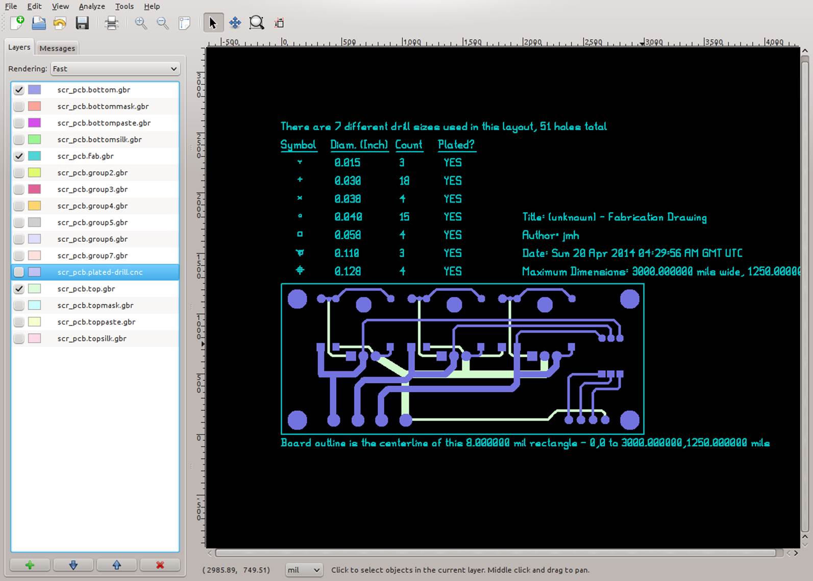
Figure 15-12. Reviewing the layout using a Gerber file viewer
Fabricating a PCB
If at all possible, consider using a low-cost PCB fabrication service instead of attempting to do it yourself. If you’ve never done it before, you might be surprised at just how difficult it can be to get everything right the first time. See Appendix D for a list of PCB fabrication service providers.
If you are lucky enough to have access to a PCB router, the Gerber files generated as part of the layout process can be used to direct the router. This is a quick way to make small PCBs, but it has some drawbacks. First, a routed double-sided PCB will not have plated-through vias, which means that each via will need to have a piece of wire soldered into it on both sides of the board and then trimmed close to the PCB. Secondly, if the layout has a lot of open space between traces, then the router is going to spend a lot of time just cutting up and discarding copper. Lastly, the holes in the PCB must be manually drilled (usually, unless the router is a very fancy model).
If your PCB is a simple, single-sided design, doing it yourself using a good PCB kit might not be a bad way to go, but it has its own perils to avoid. Appendix D lists some sources for PCB kits that you might want to look into.
Etching a PCB by hand is an error-prone process that takes some time and patience to master. Each step needs to be timed correctly, the etchant needs to be mixed correctly, and the resulting board will still need to be drilled manually, just as with the routed PCB, and none of the vias will be plated. After investing in the equipment and supplies necessary (and your time, of course) to make good etched PCBs, you might find that it would have been cheaper to just pay someone to make the board for you.
If you do elect to have your PCB produced by a commercial fabrication house, then generally all that is needed is a set of Gerber files and some money. Be aware, however, that some PCB fabricators want you to use the tools they supply (usually free of charge) and might not be too eager to work with Gerber data files generated by a nonproprietary layout editor. If the reasoning for this is based on consistent data quality in a format that is easy for the fabricator to process, and thereby hold down costs, then this approach could be justified. You will need to decide if you want to be tied to a particular layout tool, or if you want to pick your own tool.
PCB Guidelines
This section is by no means an exhaustive list of PCB layout guidelines, just a minimal set to help get you on the right path. As stated earlier, PCB layout is an art form, and it is also a science. When dealing with circuits that involve high-frequency RF or large switched currents, PCB layout designers must take into account things like capacitive and inductive coupling, trace inductance, stripline inductance and coupling, trace heating due to resistance, and other effects. However, for most low-voltage, low-current circuits, these don’t play a big role in the layout design, and just following some general common-sense guidelines can help you avoid some common mistakes and get a good end result.
If your PCB layout tool came with a user’s manual, it would be a good idea to read it. It might contain some useful information, not only about the tool itself but also about PCB layout techniques in general. Another resource is, of course, the Internet, where you can find numerous tutorials on the subject.
Layout Grid
Use the snap-to-grid feature of your layout tool. While not absolutely essential, it’s there to help position parts accurately and neatly on the PCB and make sure that features, such as mounting holes, end up where they are supposed to. The use of a grid also helps with small, dense PCB layouts, where every bit of space counts and trace spacing needs to be tightly controlled.
Grid Spacing
There are different opinions on grid spacing, with some sources suggesting 0.05 inch, others advocating 0.10 inch, and some suggesting .02 inch grid spacing. The grid selected for a layout tool is important, because it will determine how accurately parts can be positioned on the PCB layout. I typically use a 0.1-inch grid when working with a layout that involves conventional through-hole parts and components that have leads or pins spaced at 0.1 inch. For surface-mount components, I usually switch to a finer grid, on the order of 0.005 inch or 0.01 inch to accommodate the smaller parts. The downside to using a fine pitch grid is that it sometimes becomes invisible when the layout drawing is zoomed out.
Location Reference
Some tools define the lower-left corner as the (0, 0) origin point, or home location. Other tools use the upper-left corner, and still other tools let you define it yourself. In some cases, the selection of the origin for the layout can have a bearing on how the drill file will be interpreted. I typically use whatever the layout editor defines as the default, unless the PCB fabrication house has a specific requirement for origin location.
Trace Width for Signals
Try to keep signal traces at least 10 mils (0.01 inch) wide, if at all possible. Although some fabricators support trace widths down to 7 mils, production quality can be tricky to maintain with very narrow traces.
Trace Width for Power
Traces carrying power need to be wider, to provide a low resistance path for the current. The width is also dependent on the thickness of the copper cladding applied to the substrate, as a heavier copper clad is able to safely conduct higher current. Table 15-1 shows some very conservative rough guidelines for a PCB with 1 oz. copper cladding.
|
Width |
Power |
|
0.010” (10 mils) |
0.1 A |
|
0.015” (15 mils) |
0.3 A |
|
0.020” (20 mils) |
0.5 A |
|
0.025” (25 mils) |
0.7 A |
|
0.050” (50 mils) |
1.5 A |
|
0.100” (100 mils) |
3.0 A |
|
0.150” (150 mils) |
5.0 A |
|
Table 15-1. Trace widths and power |
|
These numbers are only suggestions and are not set in stone. If you do the calculations, you will find that the calculated current values are higher, but that doesn’t leave any margin. If your circuit will be operating in a high-temperature environment (e.g., alongside the engine of an automobile or in an enclosure that sits in the sun all day), using wider trace widths can help reduce possible failure due to thermal stress in the power traces. A Google search will turn up numerous trace width calculators.
Trace Separation
Keep signal traces separated by at least 10 mils, if possible. For traces that will be carrying significant current (I > 100 mA) that will be switched on and off, you might need even more separation to avoid inductive coupling into nearby traces. One way around this is to route traces carrying switched current near ground traces or ground areas on the PCB. The grounded traces and copper areas act as a shield for the potentially noisy traces.
Via Size
Most PCB layout tools come with predefined via sizes. As with traces, use a larger via if it is carrying power from one layer to another. The minimum via size is usually specified by a PCB fabricator, based on what its in-house process can reliably produce. For most cases, you can use something like a 20 mils diameter hole, although 10 mils is also used. For example, the PCB tool used to create the layout illustrations in this chapter uses a default 20 mil via with an 8-mil thick annular ring, so the entire via diameter is 36 mils. For most situations, this is fine and most PCB fabricators should be able to handle it. For more information, check the documentation for your PCB layout tool and review the requirements for the PCB fabricator you plan to use (if any).
Via Separation
As with traces, vias should be separated from traces, pads, and other vias by at least 10 mils, if possible, although in some cases you can use a 7- or 8-mil separation for really tight layouts.
Pad Size
The size of the pads used for a particular part is usually specified as a fundamental part of the component layout definition in the tool’s library. It doesn’t hurt to check it, however, because whoever defined the part might have a different idea about pad size than what your design calls for. This is particularly true if you need to run traces between the pads of something like a DIP IC, or a TO-220 transistor. Most layout tools allow you to adjust the size of the pad’s annular ring surrounding the hole, but you should not go below about 7 mils in thickness.
Sharp Corners
In general, you should avoid sharp (90 degree) corners, if for no other reason than they can be a problem during PCB fabrication (depending on the process). There is also a school of thought that claims that a sharp corner can radiate high-frequency electromagnetic energy and create interference in other parts of the circuit. Some studies have shown that this wasn’t as big of an issue as was once thought. Still, in general, it’s good practice to create a bend with a pair of 45-degree corners rather than a single 90-degree corner.
Silkscreen
If you are planning to have top (or also bottom) silkscreen designs on your PCB, be sure to avoid having the silkscreen go over any part of the board that will be exposed, such as pads or bare metal areas.
Summary
Creating a PCB is a process of translating a schematic into a physical object that uses current flow to perform a function. This chapter covered the basics of what a printed circuit board is made of and how you go about designing the pattern of wiring traces and mounting locations needed for the various components that will be soldered onto it. We also took a brief tour of the history of the PCB and showed how advances in electronics fabrication technology have led to the sophisticated, compact, and inexpensive (relatively speaking) devices that we use today.
This chapter is only the tip of the iceberg, so to speak. Entire reference books have been written on the subject of PCB design, and if you plan to do a lot of layout work, it might be a good idea to invest in one or two of the better ones. Another key point of this chapter is the necessity of practice. PCB layout is, in many ways, like learning to draw or paint. Your first attempts might look crude, but they will improve over time if you stick with it and gain the necessary skills and experience.
All materials on the site are licensed Creative Commons Attribution-Sharealike 3.0 Unported CC BY-SA 3.0 & GNU Free Documentation License (GFDL)
If you are the copyright holder of any material contained on our site and intend to remove it, please contact our site administrator for approval.
© 2016-2026 All site design rights belong to S.Y.A.