Biologically Inspired Computer Vision (2015)
Part II
Sensing
Chapter 7
Biomimetic Vision Systems
Reinhard Voelkel
7.1 Introduction
Biomimetics, combined from the Greek words bios, meaning life, and mimesis, meaning to imitate, is the imitation of the models, systems, and elements of nature for the purpose of solving complex human or technical problems [1]. How could nature inspire an engineer designing next generations of camera and computer vision systems? This depends on the application and restrictions for space and resources. If size, costs, computing power, and energy consumption do not matter, the task is relatively simple. The engineer will combine leading edge components and build a bulky expensive system providing high speed and high resolution. When the vision system needs to be very small, very fast or has to operate with minimum resources, the task gets more challenging. Then, nature is an excellent teacher. The smaller a creature is, the more expensive vision becomes for it and the more carefully the animal vision system needs to be adapted to size, brain, metabolism, and behavior [2]. Nature has done a great job in optimizing animal vision systems to the very limits.
The oldest known animal vision systems date back to the Cambrian period, about 530 million years ago. In the Cambrian period, also referred to as the “age of the trilobites”, life on earth made a huge jump forward and a rich fauna of animals evolved. This phenomenon is usually known as the Cambrian explosion. A very likely scenario is that the appearance of the first eyes was the trigger for this radical evolutionary event. Visually guided predation could have caused soft-bodied wormlike creatures of the Precambrian period to evolve to much larger, essentially modern types of animals. Vision might have created a tremendous selection pressure on all species to either quickly evolve vision themselves or at least evolve protective measures such as body armor, high mobility, or other sensors. Eyes might have been the decisive key enabling technology triggering the radical evolution of all species. From simple ocelli to large vertebrate eyes, a large variety of animal eyes evolved within this short period of only 5 million years [2]. Astonishingly, most of the intermediate solutions in eye evolution are still used today. In technology, a user will always opt for the highly developed end product. In nature, only larger animals opted for high-resolution large field-of-view (FOV) single-aperture eyes. Typically, the smaller an animal is, the more primitive the animal's eye system is. This is related to the “scaling law of optics,” stating that scaling down of a lens system drastically reduces its performance [3]. The scaling law of optics explains why it is so difficult to design miniaturized vision systems.
Understanding the scaling law of optics is mandatory for all engineers designing vision systems. Especially, as scaling down of optics follows different rules than scaling down in electronics. In electronics, scaling down of components and electric wiring is a very powerful strategy to improve the performance. Computers have evolved from room-filling and low-performance to highly miniaturized, lightweight, and very powerful devices. Over the last 50 years, the semiconductor industry has made incredible progress by making electronics smaller and smaller, down to the very limits, the atomic level. Following this success story, it would be logical to suppose that scaling down of optics would allow a miniaturized camera with very high resolution to be built. However, optics does not scale like electronics. The miniaturization of a vision system always means a significant loss of image quality and fidelity [4]. Miniaturizing the pixels of an image sensor below the wavelength is useless. Scaling down optics and building perfect miniaturized computer vision systems require different strategies. Nature has struggled with the scaling law of optics for 530 million years and, for example, replaced single-aperture eye by cluster or compound eyes. This is the main focus of this chapter. How natural concepts for miniaturization could be imitated for building computer vision systems with perfect adaption to small size, special tasks, and specific applications.
7.2 Scaling Laws in Optics
7.2.1 Optical Properties of Imaging Lens Systems
The basic parameters of a lens system are the lens pupil diameter D, the focal length ƒ, and the size XY of the image sensing unit, as shown schematically in Figure 7.1. The power of a lens is given by its ƒ-number ![]() , defined as the ratio of focal length ƒ to lens pupil diameter D and proportional to the reciprocal of the numerical aperture
, defined as the ratio of focal length ƒ to lens pupil diameter D and proportional to the reciprocal of the numerical aperture ![]() . The smallest feature a perfect lens with a circular aperture can make is the diffraction-limited spot, referred to as the Airy disk. The size of the Airy disk (diameter to the first zero) is approximately
. The smallest feature a perfect lens with a circular aperture can make is the diffraction-limited spot, referred to as the Airy disk. The size of the Airy disk (diameter to the first zero) is approximately ![]() , thus related to the lens diameter D, the focal length ƒ, and the wavelength λ only. For the photographic lens shown in Figure 7.2(a) with ƒ-number ƒ/2.8, the size of the diffraction-limited spot is
, thus related to the lens diameter D, the focal length ƒ, and the wavelength λ only. For the photographic lens shown in Figure 7.2(a) with ƒ-number ƒ/2.8, the size of the diffraction-limited spot is ![]() using green wavelength where our eyes and most image sensors see most brightly.
using green wavelength where our eyes and most image sensors see most brightly.
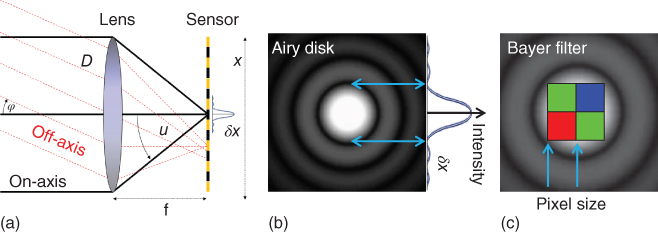
Figure 7.1 (a) Scheme of a lens with lens pupil diameter D, focal length ƒ, and angle u for the maximum cone of rays contributing to the focal spot δ× (Airy disk); (b) intensity distribution Airy disk free of aberrations; and (c) 2 × 2 pixels of image sensor with Bayer color filter covering the size of the Airy disk.
The diffraction limit is the fundamental limit of resolution for lens systems. In practice, the performance of a lens system is further reduced by aberrations, like distortion, spherical aberration, coma, astigmatism, and defocus. Unfortunately, these aberrations scale with the second, third, or even fourth power of sin(u). A “fast lens” system with a small ƒ-number of ƒ/1.4 requires very elaborate and expensive aberration corrections. Aberration correction is achieved by multiple lenses of different forms and glass material, as shown in Figure 7.2(a) and (b). For perfectly corrected lens systems, the image disturbance due to aberration is smaller than the size of the diffraction-limited spot for the full image field. The lens is referred to as diffraction limited.
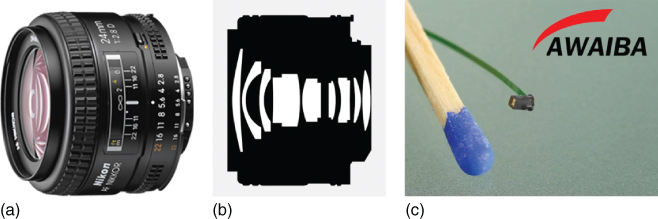
Figure 7.2 (a) Photographic lens (Nikon) with focal length ƒ = 24 mm and ƒ-number of ƒ/2.8, often written as 1 : 2.8; (b) schematic view of the optical design of the photographic lens shown (a); and (c) a pair of miniaturized NanEye cameras (Awaiba) with ƒ/2.7, a focal length ƒ = 0.66 mm, and a lens diameter of D = 0.244 mm.
For the sake of simplicity, it is assumed that each diffraction-limited spot, that is, each Airy disk, is captured by a matrix of 2 × 2 pixels of the image sensor, as shown in Figure 7.1(c). For square image pixels, the hypotenuse of each pixel will then be ![]() . For color detection, each pixel of the 2 × 2 matrix is equipped with a color filter. In practice, a 2 × 2 Bayer filter, consisting of two green, one red, and one blue filters, is applied. The usage of two green elements mimics the physiology of the human eye and the wavelength sensitivity curve of image sensors where the green light detection offers highest brightness.
. For color detection, each pixel of the 2 × 2 matrix is equipped with a color filter. In practice, a 2 × 2 Bayer filter, consisting of two green, one red, and one blue filters, is applied. The usage of two green elements mimics the physiology of the human eye and the wavelength sensitivity curve of image sensors where the green light detection offers highest brightness.
7.2.2 Space Bandwidth Product (SW)
The smaller a lens is, the easier it is to achieve diffraction-limited performance. This will be illustrated for the examples of the two different camera systems shown in Figure 7.2: (a) a large photographic camera lens and (c) a miniaturized camera for stereoendoscopes. Both lenses have an equal FOV, equal ƒ-numbers of ƒ/2.8, and an equal diffraction-limited image spot size around 4 µm for green light. In this case, the number of diffraction-limited pixels of the photographic lens is about 54 million pixels (6000 × 9000) for an image field of 24 mm × 36 mm. The sharpness of the image is significantly higher than the spatial resolution of today's top-level digital photographic cameras providing 36 million pixels with approximately 5 µm size. The photographic lens consists of 9 lens groups with a total of 13 lenses, shown schematically in Figure 7.2(b). For the miniaturized NanEye camera, shown in Figure 7.2(c), the number of recorded image pixels is 62 thousand pixels (250 × 250). The NanEye camera consists of a simple plano-convex lens and a pupil. Both lenses have the same diffraction-limited resolution. The miniaturized lens is much easier to manufacture, but the number of image pixels is drastically reduced. Scaling down of a vision systems impacts the transmitted information about the object space [3, 5]. This relationship is referred to as the space–bandwidth product (SW) and shown schematically in Figure 7.3.
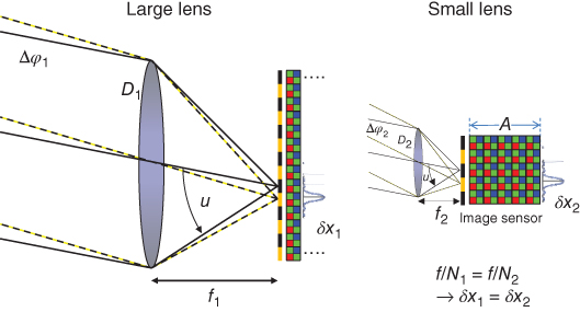
Figure 7.3 Schematic illustration of the scaling law of optics. Lenses with an equal ƒ-number have an equal best focused diffraction-limited spot of δx size (Airy pattern). Thus, the smallest resolved feature in the image is independent from the lens scaling for different lenses with an equal ƒ-number. However, the number of resolvable pixels in the image plane, also referred to as space–bandwidth product (SW), is drastically reduced for a small lens, as the size of the image scales with the lens size.
The scaling law of optics is a fundamental restriction in designing cameras for consumer applications like smartphones or tablets. Due to industrial design constraints, the overall package of a mobile phone camera should not be thicker than 5 mm, leading to focal length ƒ < 4 mm. This constraint limits the lens diameter to D ≈ 1.4 mm for ƒ/2.8. Typically, the corresponding image sensors are around 4 mm × 3 mm with a pixel size from 1.4 to 1.75 µm. This example illustrates why it is impossible to build mobile phone cameras with more than 10 megapixels and fit them into a package of less than 5 mm height. Customers' demands for higher and higher resolution of mobile phone cameras require new strategies for image capturing, for example, using camera arrays. In Section 7.3.4, will be explained how nature has perfectly mastered this size–resolution restriction for jumping spiders.
7.3 The Evolution of Vision Systems
The very basic unit of every vision system is the light-sensing unit, the sensor that converts the incident light to electrical signals. Whereas plants and bacteria have evolved a variety of different light-harvesting and light-sensing molecules, all animals share the same absorber, the opsin protein. Thus, it is very likely that the last common ancestor of all animals evolved a light-sensing opsin long before eyes appeared in the Cambrian period [2]. The simplest form of an eye is a single or multiple photoreceptor cells, referred to as an eye spot, which can only sense the presence of ambient light intensities. The animals can distinguish light from dark. This is sufficient for animals to adapt to the circadian rhythm of day and night. The technical equivalent to eye spots is the ambient light sensor in consumer products like smartphones and tablets. Their only purpose is to augment or dim the brightness of the display for optimum visibility with minimum energy consumption. The next step in the evolution of animal eyes is a pit eye, where the photoreceptor cells are caved into a cup shape. The cup of the pit eye shields the light-sensitive cells from exposure in all directions except for the cup opening direction. An enhancement of the light direction detection is the pinhole camera eye, a pit eye, where the edges of the cup go together to form a small opening. The size of the pinhole defines the angular resolution, an array of photoreceptors form the retina. Small pinholes correspond to a high resolution, but low light passes through the pinhole. To protect the inner chamber of the pinhole camera from contamination and parasitic infestation, a transparent cell closing the pinhole evolved. These transparent cells then evolved to a lens able to collect light more efficiently.
Figure 7.4 shows schematically the evolution of eyes from (a) a simple photoreceptor to (b) a pit or pinhole eye, (c) a high-resolution focused camera-type eye, and (d) a reflector eye for low-light environment [2].
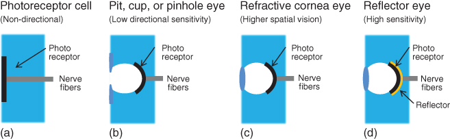
Figure 7.4 Eye evolution from a simple one-cell photoreceptor to a high-resolution focused camera-type eye. It is assumed that the whole process of eye evolution was accomplished in less than 400 000 generations.
(Modified from Land [2].)
Interestingly, all intermediate solutions are still represented in animal species living today. This is surprising. Why did selection pressure not force all animals to develop a perfect high-resolution eye? Regarding the costs for making eyes, the required brain power for vision, and the scaling laws for optics relating resolution with eye size, it is well understandable that not every creature on this planet can have high-resolution eyes. The smaller a creature is, the more expensive is its vision. The smaller a creature is, the more carefully the eye needs to be adapted to size, brain, metabolism, and behavior. Thus, eye evolution stopped at different stages for different types of animals. However, all intermediate solutions are also fully operational “end products.” They are fully operational vision systems which help the specific animal to improve its fitness for evolution and to survive. Still today, eyes are the most important sensory organ for many animals, providing detailed information about the environment both close up and far away [2].
7.3.1 Single-Aperture Eyes
The human eye is a single-aperture image capturing system similar to photographic or electronic camera systems, as shown schematically in Figure 7.5. The eye consists of a flexible lens for focusing, a variable pupil (iris) for fast sensitivity adaptation, and the retina, the image detector. A nice definition of the human eye is given by Hofmann [6]: “The human eye is a special version of a pin-hole camera, where Fresnel diffraction is compensated by the introduction of a focusing system.” The diameter of the pinhole or iris is variable from 1.8 to 8 mm for bright light and dark viewing. The lens of the human eye is spherically overcorrected by graded index effects and aspherical surface profiles. The refractive index of the lens is higher in the central part of the lens; the curvature becomes weaker toward the margin. This correction offsets the undercorrected spherical aberration of the outer surface of the cornea. Contraction or relaxation of muscles changes the focal length [7].
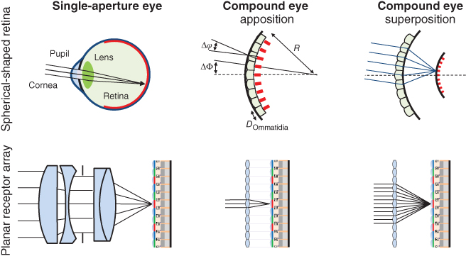
Figure 7.5 Different types of natural eye sensors and their artificial counterpart. Artificial eye sensors are based on planar components due to manufacturing restrictions.
The retina contains nerve fibers, light-sensitive rod and cone cells, and a pigment layer. There are about 6 million cones, about 120 million rods, and only about 1 million nerve fibers. The cones of the fovea (center of sharp vision) are 1–1.5 µm in diameter and about 2–2.5 µm apart. The rods are about 2 µm in diameter. In the outer portions of the retina, the sensitive cells are more widely spaced and are multiply connected to nerve fibers (several hundred to a fiber). The field of vision of an eye approximates an ellipse about 150° high by about 210° wide. The angular resolution or acuity ΔΦ is around 0.6–1 min of arc for the fovea [7].
7.3.2 Compound Eyes
Compound eyes are multiaperture optical sensors of insects and crustaceans and generally divided into two main classes: apposition compound eyes and superposition compound eyes, as shown schematically in Figure 7.5. An apposition eye consists of an array of lenses and photoreceptors each of the lenses focusing light from a small solid angle of object space onto a single photoreceptor. Each lens–photoreceptor system is referred to as ommatidia (Greek: ommation meaning little eye). Apposition eyes have some hundreds up to tens of thousands of these ommatidia packed in nonuniform hexagonal arrays [8] (Figure 7.6).

Figure 7.6 Compound eyes of dragonflies (Anisoptera).
The superposition compound eye has primarily evolved on nocturnal insects and deepwater crustaceans. The light from multiple facets combines on the surface of the photoreceptor layer to form a single erect image of the object. Compared to apposition eyes, the superposition eye is more light sensitive. Nature has evolved two principal optical methods to create superposition images: gradient refractive index and reflective ommatidia [2]. Some insects use a combination of both types of compound eyes. Variable pigments switch between apposition (daylight) and superposition (night) or change the number of recruited facets making up the superposition image [9]. A very interesting modification is the neural superposition eye of a housefly, where each ommatidium has seven detector pixels or rhabdomeres. Signals of different adjacent ommatidia interact within the neurons of the fly's brain system. This allows fast directionally selective motion detection, which enables the housefly to maneuver perfectly in three-dimensional space [7, 10].
7.3.3 The Array Optics Concept
Array optics seems to be the appropriate solution for miniaturized vision systems in nature. Compound array eyes allow small invertebrates to obtain sufficient visual information about their environment in a small eye volume with a large FOV, at the cost of comparatively low spatial resolution. These ingenious animal eyes have always inspired optical engineers. But array optics is not only a powerful design concept for miniaturization, also larger scale array optics, like camera arrays for light fields and computational photography, and even much larger array optics, like the Very Large Telescope (VLT) array for ground-based astronomy are using array configurations. The four 8.2 m diameter main mirrors, shown in Figure 7.7, work together to form a giant interferometer, the ESO's Very Large Telescope Interferometer (VLTI).
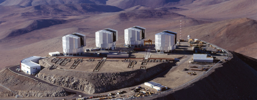
Figure 7.7 Very large telescope (VLT) Array, 4 × 8.2 m Unit Telescopes, Cerro Paranal, Chile (ESO).
Using four distant mirrors with coherent superposition should have allowed the astronomers to achieve superresolution, about 25 times higher than the resolution of the individual telescopes – in theory. In practice, it turned out to be very difficult to realize. Due to the long path and more than 30 optical elements for light guiding, less than 5% of the collected light reached the detection unit of the interferometer. The stabilization of the light path with a precision of fractions of the wavelength turned out to be almost impossible. After more than 10 years of delay to the original schedule, a first successful attempt to interfere the light from all four telescopes was accomplished in 2012, now achieving the equivalent resolution of a 130 m diameter mirror. The problems to form one integral superposition image are quite similar in the micro- and macroworld: the subimages need to fit, it is difficult to transport them to a central unit, and the superposition itself is often not trivial.
What then, is now the basic concept of array optics? A bulky and expensive one-aperture system is replaced by a multitude of smaller, flatter, or cheaper elements. Typically, these elements are arranged in a regular matrix, an array. If the arrangement is not regular, it is often referred to as a cluster. The actual scale of small does not matter much. Small could be a few micrometers and small could be the 8.2 m diameter astronomic mirror. When the performance of a one-channel system cannot be further optimized, the task is split up and distributed to a multitude of smaller units.
In a more general sense, this statement applies to all parallel systems. A similar strategy is also used in computers. Single-processor performance rose steadily from some 10 MHz in 1986 to 4 GHz in 2004 when it abruptly leveled off. Since then, the processor speeds of desktop and laptop computers range from 2 to 3 GHz, with a tendency toward multicore processors of 2, 4, 8, and sometimes even 16 cores. However, using a cluster of 16 processors does not lead to 16 times more computational power. The coordination and combining of parallel information typically reduce the achievable overall system performance. Parallel systems need a very careful design, architecture, and algorithms to be efficient. However, if a parallel system is set up properly and applied to appropriate tasks, this system could achieve superpower or superresolution, much greater than would be expected from the arithmetical sum of all individual component.
In conclusion: array optics is a beautiful concept, which allows optical designers to overcome fundamental limits of “normal” optics and to design smaller, flatter, lighter, or cheaper optical systems. However, there are some fundamental restrictions, which need to be understood before opting for array optics.
When should an optical designer opt for an array optics, a biomimetic solution? It is not easy to give a good answer. Probably, the best answer is: “Only when normal optics doesn't allow him to solve a problem.” When a classical one-aperture system is not small enough or sensitive enough, when standard single-aperture optics does not provide enough resolution or the space–bandwidth product (SW) is too low. More strictly speaking, it could be said: “never use array optics – except if you really have to.” Array optics should be used with much care and there are good reasons for this statement.
7.3.4 Jumping Spiders: Perfect Eyes for Small Animals
Looking at the eye position, two main categories could be distinguished: predators and prey. Predators tend to have eyes on the front of their head, good for focusing on a prey animal, tracking its movements and coordinating the attack. Forward-directed eyes offer a larger binocular overlap improving stereoscopic view and distance measurement. Prey animals tend to have their eyes on the side of their head, good for all round vision, allowing an attack from the side or behind to be detected. For larger animals, like a cat or a mouse, the sizes of the eye and the brain are large enough to see and detect prey or a dangerous predator. Things get more difficult if animals are very small. The main outcome of the previous section was that small animals could have sharp eyes, but their eyes will only transmit a low number of pixels, leading to very rudimentary information about the environment if a large FOV or panoramic view is required.
If now an animal is both, a predator, which requires sharp eyes and also prey, which needs to detect a potential attack from behind, things get more complicated. But evolution has developed a perfect solution for this task, the very impressive vision system of jumping spiders, shown in Figure 7.8(c). Jumping spiders (Salticidae), a family of arthropods with a body length ranging from 1 to 20 mm, have evolved amazing eyes, combining both excellent vision for hunting and a near 360° view of the world. Jumping spiders have four pairs of eyes. Two pairs are directed anteriorly to view objects in front of the spider. The visual fields of the eight eyes of a jumping spider are shown schematically in Figure 7.9 [2, 11].
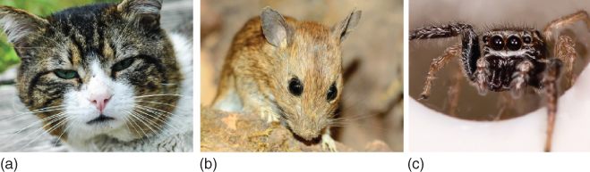
Figure 7.8 (a) Forward-directed eyes of a cat allowing stereoscopic view and direct distance measurement; (b) prey animals like the mouse have their eyes on the side allowing round vision; and (c) a male jumping spider (Pseudeuophrys lanigera). These jumping spiders live inside the houses in Europe and have excellent vision required to sight, stalk, and jump on prey, typically a smaller insects like a booklice.
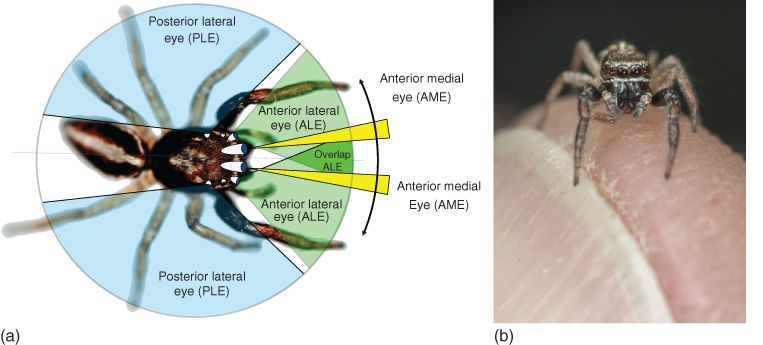
Figure 7.9 (a) Scheme of the visual fields of the four eye pairs of a jumping spider and (b) a male jumping spider (Pseudeuophrys lanigera) sitting on a fingertip.
The posterior lateral eyes (PLE) are wide-angle motion detectors which sense motion from the side and behind. The posterior median eyes (PME) are very low resolution also detecting motion. The anterior lateral eyes (ALE) are the most complex of the secondary eyes, have the best visual acuity, and provide even stereoscopic vision. They are triggered by motion and are able to distinguish some details of the surroundings. The most impressive part of the jumping spider's vision system is the anterior medial eyes (AME), the primary eyes. They are built like a telescopic tube with a corneal lens in the front and a second lens in the back that focus images onto a four-layered retina [11]. The retina of the primary eyes is a narrow boomerang-shaped strip oriented vertically and has four different kinds of receptor cells. The first two layers closest to the surface contain ultraviolet-sensitive pigments, while the two deepest contain green-sensitive pigments. The incoming green light is only focused on the deepest layer, while the other one receives defocused or fuzzy images. By measuring the amount of defocus from the fuzzy layer, the jumping spider is able to calculate the distance to the objects in front of them. The primary telescope eyes have a very high resolution, but a narrow FOV, typically 2–5° (horizontally). Unlike vertebrate eyes, the lens of the primary eye remains still. Only the retina moves. To compensate the narrow FOV, the retina of the primary (AME) eye is moved by six muscles around three axes allowing different areas to be explored, as shown (arrow) in Figure 7.9. The jumping spider observes the surroundings with its anterior lateral “wide-angle” eyes and then redirects the high-resolution anterior medial “telescope” eyes to the point of interest. Jumping spiders are diurnal hunters that stalk their prey in much the same way that a cat stalks a bird [11].
7.3.5 Nocturnal Spiders: Night Vision
Nocturnal spiders, like Deinopis, an ogre-faced or net-casting spider, have evolved very sensitive night vision (NV) eyes [2, 11]. For this, the 1.3 mm (diameter) lenses of the PME have a very small ƒ-number of ƒ/0.58. The lens is made of two components of different refractive indices for aberration correction. The photoreceptors (rhabdom) in the PME of Deinopis are around 20 µm wide, 10 times larger than in the AME of jumping spiders. A reflector layer (tapetum lucidum) behind the retina improves the light sensitivity by collecting twice-, direct-, and back-reflected light. Compared to the jumping spiders, the net-casting spiders trade resolution in better sensitivity, a perfect solution for net-casting spiders, who – as the name already indicates – catch flying insects by holding a square net between the two pairs of forelegs. As their eyes are very sensitive to sunlight, they hide in a dark spot during daytime [2, 11].
Jumping spiders and net-casting spiders, using a cluster of different single-aperture eyes, are a perfect example for miniaturization of a vision system. Dividing the vision system into different subsystems allows the tiny and lightweight spider to have three completely different vision systems: panoramic motion detection, wide angle, and telescope vision. The movable retina with a small number of pixels avoids overloading the brain with image information. Jumping spiders are able to detect prey, mates, and enemies. The movable retina allows a jumping spider track prey motionless before jumping [2, 11]. After discussing biologically vision systems in much detail, the following section focuses on the manufacturing of miniaturized optics.
7.4 Manufacturing of Optics for Miniaturized Vision Systems
7.4.1 Optics Industry
Optics manufacturing started some thousand years ago, when our ancestors polished rock crystal to manufacture loupes or burning glasses for fire making. Reading stones, a primitive plano-convex lens made by cutting a glass sphere in half, appeared in the eleventh century. The invention of spectacles or eyeglasses in the thirteenth century was the start of a first optics industry in the north of Italy. Hans Lippershey, a German-Dutch spectacle maker, filed the first patent application for a telescope on the 25th of September 1608. Building better telescopes was not only a challenge for astronomers but also very important for military purposes. Discovering and observing an enemy from a larger distance are a huge advantage for jumping spiders – and humans. Antonie van Leeuwenhoek (1632–1723) manufactured miniaturized ball lenses by melting small rods of soda lime glass in a hot flame. These high-quality glass spheres improved the resolution of his microscope viewers beyond current limits. He was the first to observe and report the existence of single-cell microorganisms, the very beginning of microbiology. Robert Hooke (1635–1703), another pioneer of microscopy, published his famous book “Micrographia,” a collection of microscope observations, in 1665 [12].
Pioneers like Carl Zeiss, Otto Schott, and Ernst Abbe significantly improved lens manufacturing and microscopy in the nineteenth century. The invention of photography further accelerated the growth of the optics industry. The optics industry was mainly dealing with large bulky lenses, but their grinding and polishing techniques were also applicable to the manufacture of miniaturized lenses for microscopes and endoscopes. Today, the optics industry provides a large variety of high-class optical elements from millimeter-scale lenses to large-scale astronomic mirrors with a surface and profile accuracy in the atomic range.
7.4.2 Planar Array Optics for Stereoscopic Vision
The development of planar array optics, also referred to as lenticular lens, lens, or microlens arrays, is much connected with photo- and cinematography. In 1908, Gabriel Lippmann invented the “integral photography,” an autostereoscopic method to display 3D images for observation with the naked eye by using a microlens array. Integral photography uses an array of small microlenses to record multiple subimages of a scene in a photographic layer. Each microlens acts like a miniaturized camera recording an individual subimage. Observing the developed photo plate through a similar lens array, the superimposed subimages form an autostereoscopic integral image, a 3D image.
Walter Hess, a Swiss ophthalmologist, learned about Lippmann's invention and founded a company to manufacture 3D photographs based on integral photography in 1914. His approach, shown schematically in Figure 7.10, was the use of cylindrical microlens arrays made of celluloid [13]. The company did not succeed and Hess continued to work in neurophysiology. It is not known how much stereoscopic vision triggered his career as neurophysiologist, but in 1949, he was awarded the Nobel Prize for mapping the different areas of the brain involved in the control of internal organs. Still today, where 3D cinemas are booming, stereoscopic vision and its influence on human brains are not fully understood. Watching 3D films is quite a challenge for the brain, and frequently, people get sick and have to leave the cinema. The problem for the brain is the mismatch of focus and convergence. The eyes are focusing on the projection screen or display, while the eyeballs follow the 3D action and converge in another plane. Lippmann's invention of integral photography is also used for plenoptic cameras.
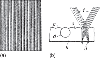
Figure 7.10 Schematic drawing (a) top view and (b) enlarged cross section of a cylindrical microlens array on a photographic layer for integral photography as proposed by Walter Hess in 1912 [13].
7.4.3 The Lack of a Suitable Fabrication Technology Hinders Innovation
Over the last 100 years, many researchers published and patented inventions, where planar array optics was the decisive key element. Often, they were brilliant ideas, but only few of them could be realized and even fewer were a commercial success. For the early lens array applications, the insurmountable entrance barrier was the availability of suitable microoptical elements for reasonable costs. At that time, microlens arrays and diffractive gratings were usually engraved or polished, for example, on a lathe. This piece-by-piece fabrication was very time-consuming and expensive, and the arrays were not very uniform. Later, glass molding, casting, and pressing were used, for example, to manufacture fly's eye condensers for slide and film projectors. Often, the quality of these microlens arrays remained poor. Surface roughness, defects, lens profile accuracy, and nonuniformities in the array constrained their field of application to illumination tasks. For more sophisticated applications, requiring, for example, a stack of two or three microoptics layers, the lateral mismatch (grid imperfections) and the array-to-array alignment were problematic. Using microlens arrays was considered to be an exotic idea usually not leading to success. The situation changed with the rapid progress of microstructuring technology in the second part of the last century, when wafer-based manufacturing was promoted by the semiconductor industry.
7.4.4 Semiconductor Industry Promotes Wafer-Based Manufacturing
In the semiconductor industry, the term “wafer” appeared in the 1950s to describe a thin round slice of semiconductor material, typically germanium or silicon. The breakthrough for planar wafer manufacturing in semiconductor industry came with the invention of the “planar process” by Jean Hoerni in 1957. The next decisive invention was to connect these transistors and form integrated circuits (IC) or microchips. Robert Noyce, cofounder of Fairchild and later Intel, patented his planar IC in 1959, and Fairchild started IC manufacturing in 1960. Hundreds, thousands, later millions, and today billions of electronics components could now be manufactured in parallel. Replacing discrete piece-by-piece electronics fabrication by Fairchild's planar process revolutionized the semiconductor industry. This was the start of the IC explosion in what is now called Silicon Valley, which created tens of thousands of new workplaces within only a few years. Semiconductor industry had a major impact on both essential parts of a miniaturized vision system, the lens, and the image sensors. Regarding biomimetic vision systems, the dominance of semiconductor technology is also one of the major restrictions for system designers. Wafers are 2D – planar. Manufacturing of microoptics and image sensors is restricted to two dimensions. Natural animal vision systems consist of 3D components like a graded index lens and a half-sphere-shaped retina. It is difficult to transfer 3D ideas to a 2D technical world.
7.4.5 Image Sensors
The photographic process, based on silver halide crystals, was the dominant image recording technology from its invention in the 1820s until the appearance of electronically recorded TV images a century later. The progression of image sensors from video camera tubes to charge-coupled devices (CCD) and active pixel sensors (CMOS) is inextricably linked to the success of wafer-based manufacturing in semiconductor industry. An image sensor is, in simple terms, an array of tiny solar cells, each of which transforms the incident light into an electronic signal. In CCD sensors, the charge is transported across the chip, read out at one side, and converted into a digital value. In CMOS devices, the electronic signal is amplified by transistors, located beside the receptor, and the signal is transported by electric wires. Until recently, CCD sensors were credited to have less visual noise and distortion and were preferred for high-quality image capturing. CMOS (Complementary metal-oxide semiconductor) sensors have now taken the lead. CMOS sensors are significantly cheaper than CCD, they are faster, and backside-illuminated CMOS sensors make them more sensitive for low-light situations. Another advantage of CMOS image sensors is that they are manufactured with standard microprocessor technology allowing reuse of obsolescent semiconductor fabs for their production.
In a front-illuminated image sensor, a matrix of transistors (active pixel sensors) and metal wiring is placed in front of the photosensitive layer. This maze of wires and transistors blocks a part of the incident light, as shown schematically in Figure 7.11(a). In backside-illuminated image sensors, the transistor matrix and wiring is moved behind the photosensitive layer, as shown in Figure 7.11(b). A 100% fill-factor image sensor with improved low-light sensitivity is obtained. For the manufacturing of backside-illuminated sensors, the wafer with the CMOS image sensor is flipped and the silicon is thinned from the backside, until it is thin enough to let the light shine through.
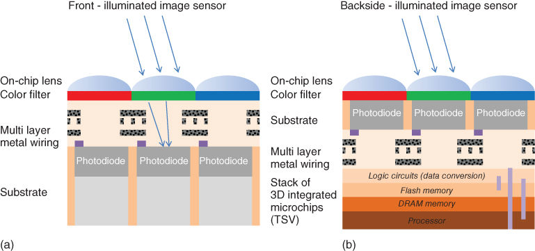
Figure 7.11 (a) Front-illuminated image sensor and (b) backside-illuminated image sensor bonded to a stack of a 3D integrated chips with through-silicon via (TSV) connections.
Interestingly, nature also evolved similar 100% fill-factor retinas for the eyes of cephalopods, active marine predators like the nautilus and the octopus. In the human retina, the nerve fibers are before the retina, blocking light and creating a blind spot where the fibers pass through the retina. In cephalopod eyes, the nerve fibers route behind the retina layer, very similar to the backside illumination image sensor.
Beside the higher sensitivity, the backside illumination CMOS sensor technology has another huge advantage compared to the CCD sensor. As shown in Figure 7.11(b), the image sensor could be bonded to a stack of other thin electronic layers (processors, memory, etc.). Through-silicon via (TSV) connections allow signals and data to be transferred vertically through the different electronic layers. Wafer-thinning, wafer-level stacking, or wafer-level packaging (WLP) technologies are referred to as 3D IC manufacturing. The new 3D IC trend in microelectronics is likely to have a grand impact on future generations of CMOS image sensors. Integrated 3D CMOS image sensors, using highly parallel data treatment, transport, and on-sensor storage, will provide ultrahigh-speed, low-noise, high-dynamic range (HDR), and hyperspectral image sensors in a small package at low costs.
7.4.6 Wafer-Based Manufacturing of Optics
The manufacturing of miniaturized optics by using classical optics manufacturing technologies, like grinding and polishing, is possible but very cumbersome and expensive. The rise of the wafer-based semiconductor industry also had a considerable impact on microoptics manufacturing [14]. In the mid-1960s, Adolf W. Lohmann made the first step by combining computers, plotters, and photolithography to manufacture computer-generated holograms (CGH). In the 1970s, dry plasma etching technology was introduced for the transfer of microoptical structures from structured photoresist into glass wafers. In the mid-1980s, Zoran Popovic proposed a microlens fabrication technology based on microstructuring of the photoresist by photolithography and a subsequent resist melting process, as shown in Figure 7.13.
Planar optics, the integration of different optical functions on one planar substrate, was one of the most promising future technologies in the 1980s. Optics, later relabeled as photonics, hoped to repeat the semiconductor hype in generating infinite growth and wealth of a planar optics industry, similar to the IC explosion in Silicon Valley. The first companies manufacturing microoptics on wafer scale appeared in the 1990s. However, neither the optical computer nor the later photonics hype really took off. Planar optics could not redo what semiconductor industry had done. The fundamental difference is that electronics allows complete devices to be built – including the input sensor, CPU, memory and output, a display, sound, or movement. Optics and microoptical elements are typically only parts of a larger mechanical or electronic device used to redirect, shape, or switch the light. But planar microoptics is a decisive key enabling technology for miniaturization of optical systems, like vision systems.
7.4.7 Manufacturing of Microlens Arrays on Wafer Level
Microlens arrays appeared already in the Cambrium. Trilobites, shown in Figure 7.12(a), a fossil group of marine arthropods, had complex compound eyes with microlenses made of calcite. Still today, similar compound eyes are found in many small creatures. Refractive microlens arrays seem to be an appropriate solution for miniaturized vision systems in nature.
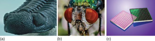
Figure 7.12 (a) Trilobite eye – microlens arrays made of calcite, (b) compound apposition eyes of a fly, and (c) microlens array manufactured by wafer-based technology in quartz glass (fused silica) [14].
How to manufacture refractive microlenses and microlens arrays for biologically inspired vision sensors? Many technologies have been developed to generate arrays of small lenses. The most accurate, and therefore widely used in industry, is the melting resist technology [14], shown schematically in Figure 7.13. The melting resist process is also used for on-chip microlenses on the CMOS image sensor pixel, as shown in Figure 7.11. Here, the microlenses are not used for imaging, they are used for fill-factor enhancement, funneling the incident light onto the photosensitive layer.
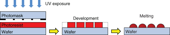
Figure 7.13 Melting photoresist technique for manufacturing refractive microlenses on wafer level.
For the melting resist process, a thick layer of positive photosensitive resist is spin coated on a glass wafer and exposed with ultraviolet light in a mask aligner. After wet-chemical development and drying, the resist structures are melted in an oven or on a hot plate. The melting procedure itself is quite simple [14]. Above the softening temperature, the edges of the resist structure start melting. Above the glass transition temperature, the amorphous resist polymer changes into a glass state system. The surface tension tries to minimize the surface area by rearranging the liquid masses inside the drop. Ideally, the resist melts completely, the masses are freely transported, and surface tension forms a spherical microlens. In practice, the lens melting process needs careful process optimization and precise control of all process parameters to obtain good lens-to-lens uniformity within one wafer and from wafer to wafer. Repeatability and uniformity of melted resist lenses are key factors for the following etch process.
In the next step, the microoptical components are transferred from the photoresist state into wafer bulk material by reactive ion etching (RIE) as shown in Figure 7.14. The etching process removes atoms from the resist and the wafer surface at different etch rates. Surface areas covered by resist structures are protected until the covering resist layer is removed.
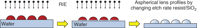
Figure 7.14 Transfer of resist microlenses into the wafer bulk material by reactive ion etching (RIE).
Melted resist microlenses are usually very close to a spherical lens profile with a conic constant around k ≈ 0 after melting. The transfer of the melted resist lens by RIE allows the lens profile to be changed. This is done by varying the mixture of the etch gases and oxygen during the etch process. If the etch rate for resist is higher than for the wafer bulk material, the resulting lens profile will be flatter than the resist lens profile. A continuous change of all etch parameters allows to obtain aspherical lens profiles.
7.4.8 Diffractive Optical Elements and Subwavelength Structures for Antireflection Coatings
Diffractive optical elements (DOEs) and gratings are manufactured on wafer level by using subsequent photolithography and sputter or plasma etching steps, as shown in Figure 7.15 for a four-level DOE [15]. A very critical process step for the manufacturing of multilevel DOEs is the proper alignment during photolithography and the precise transfer of the resist structures into the wafer bulk material.
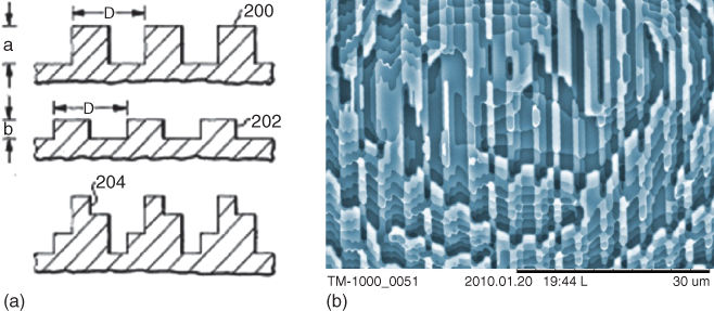
Figure 7.15 (a) Multilevel diffractive optical elements (DOE) manufactured with a planar process using subsequent photolithography and dry etching [15]. (b) Eight-level diffractive optical element in fused silica glass material.
Photolithography in wafer stepper or e-beam direct writing allows manufacturing highly efficient DOEs with minimum feature sizes smaller than the wavelength of the light. For most optical applications, it does not make sense to manufacture structures with subwavelength feature size. The light is not able to resolve the structures; the light sees a composite material of which the optical properties are between those of air and those of the base material. Nonetheless these subwavelength structures are becoming very popular as new type of antireflection (AR) coating recently [16].
When light passes through a glass surface, a part of the light – typically some 4–5% – is reflected at the surface. Photographic objectives, as shown in Figure 7.2(a), typically consist of some 10 individual lens or doublet elements comprising some 20 glass to air (or other glass material) surfaces. At each surface, some light is reflected. This light continues its path in the objective generating stray light, ghosting, and flare images. Antireflective coatings, typically thin-film structures with alternating layers of high and low refractive index, were introduced in photographic lenses in the 1970s. They significantly reduce the loss of light in lens systems and improve the contrast and imaging performance of lenses for vision systems. Unfortunately, the choice of suitable thin-film materials is very limited, and their refractive indices are close to glass.
Recently, major camera lens manufactures introduced subwavelength AR coatings, often referred to as nanoparticle, nanocrystal, or subwavelength structure coatings (SWC), for their high-end lenses. Subwavelength AR coatings have some major advantages. Subwavelength AR coatings are, for example, made of wedge-shaped nanostructures causing a continuously changing refractive index or spongy layers with variable cavity density within their volume. This allows material with a very low refractive index close to air to be manufactured. Instead of multiple layers of different material, now a continuous change of the index from glass to air is applied. This significantly reduces the losses and reflections at the lens surfaces. Today, subwavelength coatings are mainly applied to wide-angle lenses where the curve of the lens surfaces is very large.
Not surprisingly, nature had already invented subwavelength AR coatings for nocturnal insects. The corneas of some moth eyes are covered with conical protuberances of subwavelength size, providing a graded transition of refractive index between air and the cornea [17] – very similar to the novel nanocoatings for high-end photographic lenses. For these nocturnal insects, the purpose of the AR coating is twofold. Low loss of light at the cornea's surface is certainly of some importance. Much more important is the lowest possible reflection from the cornea's surface, because shining and glowing eyes could make the insect visible to a potential predator [2].
7.4.9 Microlens Imprint and Replication Processes
The wafer-based technologies using lithography and plasma etching are well suited to obtain high-quality microoptical components on wafer scale. However, these manufacturing technologies are too expensive for high production volumes. For consumer applications, the average sales price (ASP) of a miniaturized camera module is typically in the range of US$ 1–20. For mass production of wafer-level camera (WLC) lenses, the preferred technology is UV imprint lithography, using a mask aligner and photosensitive polymers [4, 18]. A microlens wafer is used as a master, copied to a PDMS stamp and then replicated into polymer on glass.
Figure 7.16 shows the basic process of UV imprint lithography in a mask aligner. A stamp is embossed in the liquid polymer, and exposure with ultraviolet light provides a quick curing of the polymer. UV imprint allows to manufacture full lens wafers in one step and to achieve high uniformity and precise lateral placement of the microlenses within the array [19]. Process improvements like prior dispensation of microdroplets on the wafer or in the stamp, as well as enhanced imprint methods, like surface conformable imprint lithography (SCIL), are applied to improve the uniformity and yield. The microlens wafers are then mounted by WLP to wafer-level optics modules [20].
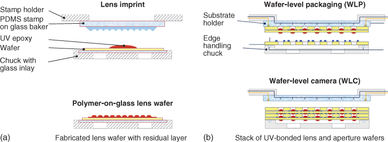
Figure 7.16 UV imprint lithography and wafer-level packaging (WLP): (a) A PDMS stamp is embossed on a wafer with a drop of a photosensitive polymer. The resist is formed by the PDMS pattern and exposed by UV light for curing. After hardening of the resist, the PDMS stamp and lens wafer are separated; (b) lens and aperture wafers are mounted in a mask aligner to obtain a stack of wafer-level cameras (WLC).
7.4.10 Wafer-Level Stacking or Packaging (WLP)
Kenichi Iga and his colleagues attracted attention in the early 1980s with their idea of stacked planar optics [21]. In the early 1990s, the first systems requiring a stack of microlens wafers were built – for example, a 1 : 1 microlens projection lithography (MPL) system for mask aligners, projecting a photomask onto a wafer located at a large distance by using some 300 000 individual lens channels [22] (Figure 7.17).
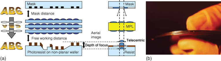
Figure 7.17 (a) Schemes of a microlens projection lithography (MPL) system for 1 : 1 projection of a photomask onto a wafer in a mask aligner and (b) photograph of an early prototype system, a stack of three microlens wafers.
The most critical process step for such wafer-level projection systems is the proper alignment of multiple wafers. Thickness variation of the wafers, bending and warp, lateral displacement, and bonding or gluing of multiple wafers could be quite cumbersome. WLP of microoptics became very popular some years ago, when industry tried to implement the WLC technology in mass production of cameras for consumer products like smartphones and tablets [4].
7.4.11 Wafer-Level Camera (WLC)
Today's mobile phone cameras consist of some 10–20 different components such as plastic- or glass-molded lenses, pupils, baffles, actuators, lens holders, barrel, filters, and the image sensor. These components are manufactured and assembled piece by piece. The WLC approach is rather simple: All components are manufactured on wafer level, the lens wafers are mounted together with the CMOS image sensor wafer, and the wafer stack is diced into some thousands of individual camera modules, as shown in Figure 7.16(b). The complete mobile phone camera, including the optics, is manufactured and packaged on wafer level using standard semiconductor technology [4].
WLC for low-cost applications such as mobile phones and disposable endoscopes had gained much popularity in industry some years ago. However, most companies failed to succeed with WLC cameras on the market. The major problem of WLC was the overall yield. A defect in one of the multiple layers makes the camera unusable leading to low yield for complete wafer stacks. Another source of problems is the restriction of the optical design. In WLC, all lenses have to be located on the front or the backside of a wafer. This is a severe handicap for the optical designer. Lenses have to be separated by the thickness of the supporting wafer. For example, it is not possible to manufacture meniscus-shaped lenses.
The first wafer level cameras (WLC) such as the one shown in Figure 7.18, combining microoptics wafers made from polycarbonate and thinned CMOS imagers (backside illumination) were developed in 2002 [23].
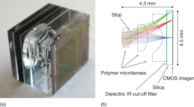
Figure 7.18 (a) Wafer-level camera (WLC) built within European Research Project WALORI in 2005 [23]. Backside illumination (BSI) through thinned CMOS image sensor, 5.6 µm pixel VGA; (b) optical design of the WLC shown (a).
The next step is wafer-level integration (WLI), combining wafer-level microoptics with optoelectronic components such as photodiodes, LEDs, or lasers arranged and mounted on wafer level. The WLI approach gained much success recently for manufacturing high-volume components integrated in the latest generations of smartphones. Several thousands of lenses or other microoptical elements can be fabricated simultaneously on a single 200 mm glass wafer. The process chain includes lithography for apertures, double-sided and aligned replication of lenses, stacking of wafers, automated optical testing, and wafer dicing. Providing miniaturized optoelectronic modules for smartphones is the key technology for future biomimetic compound vision systems.
7.5 Examples for Biomimetic Compound Vision Systems
Biomimetic compound vision systems have been investigated by numerous research teams within the last 25 years [2, 10, 24]. Artificial compound eyes have been implemented and tested for many different applications. Robots for flying and swimming have been equipped with lightweight biomimetic vision systems, enabling them to maneuver successfully in 3D space. Novel approaches to miniaturize and to improve vision systems for next generations of robots, drones, and – even more important – for automotive and consumer applications are on their way. It is impossible to cite or reference all these very interesting approaches. In the following section, a small selection of biomimetic compound vision systems is presented as examples.
7.5.1 Ultraflat Cameras
Taking pictures whenever and wherever has become standard nowadays. Miniaturized cameras, integrated in consumer devices, like smartphones, tablets, and laptops, create a permanent availability of a camera. This was not always the case.
In the beginning of photography, the photographic plates had to be developed right after the exposure. To take pictures outside their studio, the early photographers needed to be equipped with a mobile darkroom, typically a tent or a van. In 1913, Oskar Barnack built a first prototype of a Leica camera, working with standard cinema 35 mm film. His Leica camera set the standard with 24 mm × 36 mm image size on negative film and became the first permanently available consumer camera manufactured in large volume in the 1930s. The Minox, a miniaturized camera with 8 × 11 mm image size, was the first camera that could be carried around in a trouser pocket. Its small size and macrofocusing ability made it also very popular for espionage. Compact digital still cameras entered the consumer market in the mid-1990s, gradually replacing photographic film cameras. Camera phones first appeared on the market in 2002. Today, wearable cameras integrated in clothes or eyeglasses are on the rise.
An earlier approach in the pre-camera phone area was the credit card camera [24]. Besides taking pictures, a credit card camera could enhance the card security by providing embedded face or iris detection. However, the 0.76 mm normalized thickness of a credit card would require an ultraflat camera design. Obviously, a single-aperture camera system would not work out; a compound array camera design could be the only option.
In a first approach, mimicking an apposition compound eye, a single microlens array was used. Each microlens captures a different demagnified subimage as indicated in Figure 7.5. All subimages are recorded on a thin CMOS image sensor. Figure 7.19 shows (a) schematically the principle of the single microlens array imaging system and (b) the obtained subimages for an array of microlenses with lens pupil diameter D = 135 µm, focal length ƒ = 320 µm, ƒ/2.4, and 3 µm diffraction-limited spot size. In this approach, the individual images are superposed electronically to form a complete image.
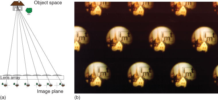
Figure 7.19 (a) Microlens array camera imaging individual subimages from an object to an image plane and (b) recorded subimages for ƒ/2.4 array camera.
In a more complex approach, mimicking a superposition compound eye, a stack of three microlens arrays, as shown schematically in Figure 7.20(a), was used. The lenses of the first array image demagnify and invert subimages of the object into the plane of the second lens array. The lenses of the third array image these inverted subimages to the image sensor plane. The lenses of the second array serve as field lenses, imaging the pupil of the first array to the corresponding entrance pupils of the third lens array. As shown in Figure 7.20(a), size, focal length, and distances in the system are optimized to obtain correct superposition of the individual subimages in the plane of the image sensor.
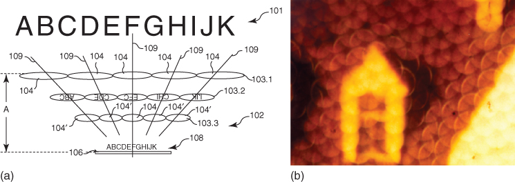
Figure 7.20 (a) Ultraflat camera system consisting of three layers of microlens arrays and (b) superposition of individual subimages obtained from a 1 : 1 multichannel imaging system as shown in Figure 7.16, imaging the same object also shown in Figure 7.18.
Integrating a camera in a credit card is obsolete since camera phones have taken over the consumer market. However, both the apposition and the superposition version of the proposed ultraflat cameras are still investigated today [25, 26].
Future applications are, for example, large-object field microscopes, shown in Figure 7.21. If it becomes possible to build ultrathin and flexible cameras, a large range of possible products comes into sight.
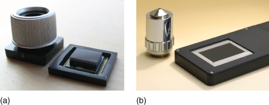
Figure 7.21 (a) Electronic cluster eye (eCLEY) with a FOV of 52° × 44° and VGA resolution, an apposition compound design with electronic superposition and (b) an ultrathin array microscope with integrated illumination, a superposition compound vision design. Both devices are built at Fraunhofer IOF in Germany. Both photos compare the biomimetic vision system (right in the photos) to the standard optics, a bulky objective, and a standard microscope [24, 25].
7.5.2 Biologically Inspired Vision Systems for Smartphone Cameras
The eight-eye vision system of jumping spiders, shown in Figure 7.9, seems to be the optimum solution nature evolved for small animals: 360° panoramic motion detection, a wide-angle viewing capability to identify prey or an enemy, and a high-resolution vision with a range finder to track a target to jump on. These three different vision systems are integrated in a small lightweight spider body and operated by a tiny brain.
What then, is the perfect solution for future miniaturized cameras to be integrated in future consumer products? Making a wish list, a future miniaturized vision system for consumer products should have:
· High resolution, preferably in the range of 50 megapixels and more
· HDR, from very low light to the bright sunlight at the beach
· High color depth
· Fast autofocus (AF) and zoom
· Stereoscopic view and detailed depth map
· High speed with 1000 frames per second
· NV and thermal imaging
It is – from the current point of view – not possible to integrate all these functions in a single vision module. Additionally, the height restriction of some 4–5 mm correlates with an achievable resolution of some 5–8 megapixels due to the limited space–bandwidth product (SBP), as discussed in Section 7.2.2. The most promising approach is to mimic the eyes of the jumping spider and to split vision to a cluster of single-aperture cameras. One interesting biologically inspired approach is the 4 × 4 PiCam cluster camera discussed in more details in the next section.
7.5.3 PiCam Cluster Camera
An interesting approach in this direction is the 4 × 4 PiCam developed by Pelican Imaging [27] and shown in Figure 7.22. All 16 cameras capture an image at the same time using 1000 × 750 pixels leading to a synthesized image of 8 megapixels after date processing. A clever trick of the PiCam cluster approach is to move the RGB color filters from the sensor pixel plane to the lens level. Three types of ƒ/3.1 lenses for red, green, and blue, a 56° (diagonal) FOV and a focal length of 2 mm are used. The total height of the camera module is less than 3.5 mm. As shown in Figure 7.22(b), the Bayer filter pattern with typically two green, one red, and one blue is applied to the camera lens level. Two green, one red, and one blue cameras form 2 × 2 subarrays.
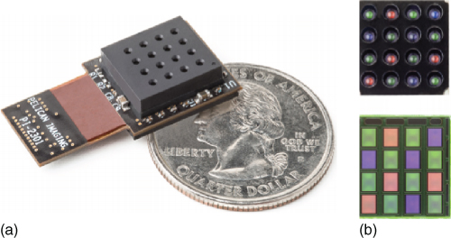
Figure 7.22 (a) PiCam module consisting of 4 × 4 individual cameras with 0.75 megapixel resolution and (b) lens and sensor array with RGB color filters (Pelican Imaging).
Using cameras with a smaller chromatic range significantly relaxes the optical design for the lenses. Reduced chromatic aberrations lead to significantly better images with fewer lenses. Preferably, the image plane is adapted to the wavelength range for the individual cameras. Avoiding a Bayer filter pattern on each image sensor pixel reduces the height of the pixel stack. As shown in Figure 7.11, a thinner pixel stack enables the pixel to accept a wider cone of incident light, thus improving the efficiency of the light capturing and reducing crosstalk and blur [27].
The hyperfocal distance, defined as the closest distance a lens can focus while keeping objects at infinity acceptably sharp, scales with the lens diameter. For the PiCam, the hyperfocal distance is 40 cm. Thus, the lens images all objects from 20 cm to infinity sharp, if the fixed focus is set to the hyperfocal distance. The parallax detection and superresolution provided by the 4 × 4 arrangement allows a postcapture refocus, similar to a light-field camera. The absence of an AF unit is not only a cost factor; it also avoids the typical AF delay in image capturing. Today, the majority of AF camera modules are based on voice coil motors (VCM) to move one or more lenses along the optical axis. A major disadvantage is that the VCM AF does not provide fixed positions. A typical AF procedure is to move the focus through all positions, capture, and analyze the resulting images. By repeating this, the best focus for the scene is obtained. A typical camera can have as many as 10–20 steps between near and far extreme focus and easily take >1 s to acquire a sharp image. This focus first and capture later procedure is quite annoying, especially for capturing quickly moving objects or scenes. The cluster camera approach of the PiCam allows a capture first and refocus later approach – a clear advantage for the user [27].
Although the cluster array concept, followed by the 4 × 4 PiCam, has very clear advantages, it remains challenging. Similar to the jumping spiders, a cluster camera requires a lot of computational power and intelligent software algorithms to compose the high-resolution images. Computation is already a problem for jumping spiders. For some jumping spiders, the brain takes up to 80% of the space in the body. To achieve superresolution, a cluster camera needs special processor hardware for ultrafast and parallel image processing. Similar to the jumping spider, cluster vision is expensive with regard to energy respectively battery consumption. The next example for biomimetic compound vision systems is related to fast movement detection, similar to the compound apposition eyes of Drosophila and dragonflies.
7.5.4 Panoramic Motion Camera for Flying Robots
Engineering a vision system for small flying robots is a very challenging task [28]. The vision system should be small, lightweight, and provide distortion-free wide FOV. For flight control and collision avoidance, the systems should be optimized for fast motion perception, meaning a low resolution to enable ultrafast data treatment using low computational power. Flying insects perfectly meet all of these requirements. Compound eyes, consisting of a mosaic of small ommatidia, offer large FOV of up to 360°. The even more impressive feature of these insect eyes is the high temporal resolution. Human vision is sensitive to temporal frequencies up to 20 Hz. Some compound eyes respond to temporal frequencies as high as 200–300 Hz [28]. This explains why it is so difficult to catch a fly. For a 10 times faster motion detection system, the movement of our hand appears in slow motion and the fly has all time to move away [2, 28].
Flying arthropods like bees, houseflies, and dragonflies have been extensively studied by biologists for decades. The compound vision and neuronal system is very well understood today. The sensory and nervous systems of flies have been mimicked as neuromorphic sensors. However, despite a deep knowledge of the vision system of flying insects, it remains very difficult to reproduce artificial systems that can display the agility of a simple housefly.
A curved artificial compound eye has been investigated recently the CurvACE research project [29], shown in Figure 7.23.
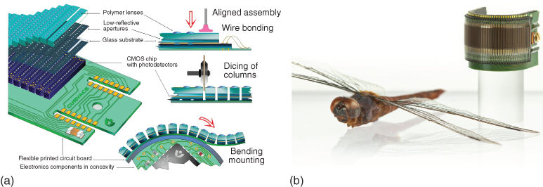
Figure 7.23 (A) Scheme of the manufacturing of a curved artificial compound eye from the research project CurvACE [29]. Polymer-on-glass lenses, apertures, photodetectors (CMOS), and interconnections (PCB) were manufactured on a flexible layer, then diced, and mounted on a rigid semicylindrical substrate; (B) image of the CurvACE prototype with a dragonfly.
The major challenge was to manufacture a miniature artificial compound eye on a curved surface, as shown schematically in Figure 7.23. Similar to a compound apposition eye, shown in Figure 7.5 (center), each ommatidia or lens channel consisted of one microlens and one corresponding image pixel on the CMOS image sensor. To reduce crosstalk, two low-reflective opaque metal layers with apertures (pinholes) were placed in between lens and pixel. The technical approach was WLP of the two optical layers (microlenses and apertures) and the CMOS image sensor chip on a flexible printed circuit board (PCB) containing the electrical interconnections. In a next step, the assembled stack was diced into columns down to the flexible interconnection layer, which remained intact. Finally, the ommatidial array was curved along the bendable direction and attached to a rigid semicylindrical substrate with a radius of curvature of 6.4 mm. Two rigid circuit boards containing two microcontrollers, one three-axis accelerometer, and one three-axis rate gyroscope were inserted into the rigid substrate concavity and soldered to the sides of the ommatidia through dedicated pads. The prototype of a curved artificial compound eye contained 630 lens channels with an interommatidial angle of around 4° providing a FOV of 180° in the curved direction. These values correspond exactly to the values of a Drosophila melanogaster compound eye, but with the only difference that the fly's eye is 10 times smaller in scale [29]. The curved artificial compound eye, shown in Figure 7.23, is a lightweight, energy-efficient, miniature vision sensor with panoramic view. The restriction to a horizontal only bending of the image sensor enables a robot to navigate in flat environments only – still a long way to go to manufacture artificial compound sensors with excellence comparable to nature – but it is a first step and it opens up new avenues for vision sensors with alternative morphologies and FOVs of up to 360° in small packages. The recent trend to develop wearable electronics and cameras will certainly help to quickly improve the CurvACE concept to achieve more elaborate bioinspired vision sensors.
7.5.5 Conclusion
Mobile phone cameras are a flagship feature of a flagship device. Customers will always opt for the better or more prestigious camera. The scaling law of optics and the related space–bandwidth product (SBW) make it difficult to manufacture a single-aperture camera with more than 10 megapixels fitting in a package of less than 5 mm overall thickness. Thus, the demand for higher and higher image quality of mobile phone cameras requires new strategies for image capturing sensor systems. The jumping spider's eye, a 4 × 2 cluster eye, is probably the best high-resolution vision system within a small package that nature developed in 530 million years. Is it possible to derive something similar in the technical world?
The pure cluster camera approach, for example, the 4 × 4 PiCam, is expensive in terms of manufacturing costs, expensive in terms of image computation hardware, and expensive in terms of energy consummation per picture taken. Another important issue for the acceptance of cluster cameras – and more generally for all computational image capturing technologies – is their inability to take pictures in critical environmental light conditions. Pure cluster cameras with computational image capturing have severe problems producing acceptable image quality in difficult lighting situations like in bright sunlight at the beach, in a room, in a nightclub, or at a concert. Scrambled or distorted images with artifacts are not acceptable for customers.
A biomimetic approach, for example, the combination of jumping spider's eye with Deinopis NV eyes, might be a better match than pure cluster cameras. The idea is to combine two cameras with different FOV: a wide-angle and a telescopic camera. Figure 7.24 shows different possible arrangements of camera modules for integration in smartphones or tablets.
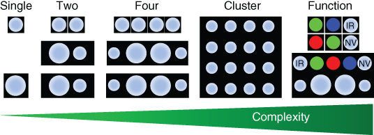
Figure 7.24 Different possible arrangements of camera modules for integration in smartphones or tablets.
Zooming from large field to small field could be achieved by combining both images. A dual camera concept also allows gives high resolution in the center of an image. Like the jumping spider, combine these two lenses with other lenses for specific tasks, for example, integrating thermal imaging (IR) in a mobile phone, as shown in Figure 7.25, or infrared front-facing cameras to detect the eyeball position to provide dynamic 3D perspective.
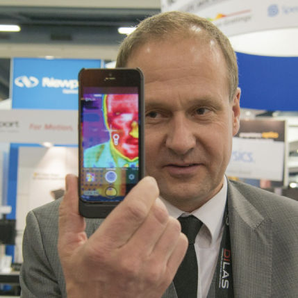
Figure 7.25 Portrait of the author performing a self-portrait using a FLIR ONE™, the first thermal imager designed for mobile phones and presented by FLIR Systems in 2014 [30].
Stereoscopic vision, range finder, NV, and thermal vision (IR) will be available for consumer products soon and will immediately become standard for cars' onboard camera systems. Detecting a deer running on collision course or a fallen tree blocking the road in the dark forest will save many lives worldwide. For mobile phone cameras, it is more difficult to predict what will be the future camera systems convincing customers to purchase next generations of mobile phones and tablets. But biologically inspired cluster eye concepts will play a decisive role, and the rapidly advancing CMOS image sensor technology will help to revolutionize miniaturized vision systems in the near future.
Image sensor manufacturers recently announced that they are working on curved image sensors with more than 20 megapixels. If this technology becomes mature, it might trigger a true revolution in imaging. For an imaging system, a flat object normal to the optical axis will be imaged to a curved image plane, the Petzval field curvature. Upto now, photographic plates, films, CCD and CMOS image sensors, and all available image capturing devices have been planar. Correcting an objective for field curvature (Petzval) is very difficult for lens designers, especially for large object and image fields. A curved image sensor would allow to be simplified the lens design significantly. Using a curved image sensor allows to design high-speed lenses with very large image fields. For example, using the optical specifications of a Deinopisnocturnal eye, that is, 1.3 mm lens diameter, ƒ/0.6, and a curved image sensor, this single-aperture lens could provide more than >10 megapixels within package of 5 mm size. If industry could also provide full-frame curved image sensors, all photographic cameras and lenses might change completely in design, size, and resolution. For now, just a dream – but imaginable.
References
1. 1. Wikipedia Biomimetics, http://en.wikipedia.org/wiki/Biomimetics (accessed 15 April 2015).
2. 2. Land, M.F. and Nilsson, D.-E. (2012) Animal Eyes, 2nd edn, Oxford University Press, ISBN: 978-0-19-958113-9.
3. 3. Lohmann Adolf, W. (1989) Scaling laws for lens systems. Appl. Opt., 28 (23), 4996–4998.
4. 4. Voelkel, R. and Zoberbier, R. (2009) Inside wafer-level cameras. Semicond. Int., 28–32.
5. 5. Ozaktas, H.M., Urey, H., and Lohmann, A.W. (1994) Scaling of diffractive and refractive lenses for optical computing and interconnections. Appl. Opt., 33 (17), 3782–3789.
6. 6. Hofmann, C. (1980) Die optische Abbildung, Akademische Verlagsgesellschaft Geest & Portig K.-G., Leipzig.
7. 7. Voelkel, R. (1999) Natural optical design concepts for highly miniaturized camera systems. Proc. SPIE, Design and Engineering of Optical Systems II, 3737, 548. doi: 10.1117/12.360049.
8. 8. Sanders, J.S. and Halford, C.E. (1995) Design and analysis of apposition compound eye optical sensors. Opt. Eng., 34, 222–235.
9. 9. Snyder, A.W. (1977) Acuity of compound eyes: physical limitations and design. J. Comp. Physiol. A, 116, 161–182.
10.10. Franceschini, N., Riehle, A., and Le Nestour, A. (1989) in Facets of Vision (eds D.G. Stavenga and R. Hardie), Springer-Verlag, Berlin, pp. 360–390.
11.11. Wikipedia. http://en.wikipedia.org/wiki/Jumping_spider, (accessed June 2014).
12.12. Hooke, R. (1665) Micrographia, J. Martyn and J. Allestry, Royal Society, London.
13.13. Hess, W.R. (1912) Stereoscopic pictures. US Patent 1128979.
14.14. Voelkel, R. (2012) Wafer-scale micro-optics fabrication. Adv. Opt. Technol., 1, 135–150. doi: 10.1515/aot-2012-0013 (Review article).
15.15. Gale, M.T., Lehmann, H.W., and Widmer, R.W. (1977) Color diffractive subtractive filter master recording comprising a plurality of superposed two-level relief patterns on the surface of a substrate. US Patent 4155627.
16.16. Lohmueller, T., Brunner, R., and Spatz, J.P. (2010) Improved properties of optical surfaces by following the example of the moth eye, in Biomimetics Learning from Nature (ed M. Amitava), InTech. ISBN: 978-953-307-025-4.
17.17. Clapham, P.B. and Hutley, M.C. (1973) Reduction of lens reflection by the ‘moth eye’ principle. Nature, 244, 281–282. doi: 10.1038/244281a0
18.18. Rudmann H, Rossi M (2004) Design and fabrication technologies for ultraviolet replicated micro-optics. Opt. Eng.; 43(11), 2575–2582.
19.19. Schmitt, H. et al. (2010) Full wafer microlens replication by UV imprint lithography. Microelectron. Eng., 87 (5-8), 1074–1076.
20.20. Voelkel, R., Duparre, J., Wippermann, F., Dannberg, P., Braeuer, A., Zoberbier, R., Hansen, S., and Suess, R. (2008) Technology trends of microlens imprint lithography and wafer level cameras (WLC). 14th Micro-Optics Conference (MOC, 08), Brussels, Belgium, Technical Digest, September 25–27, 2008, pp. 312–315.
21.21. Iga, K., Kokubun, Y., and Oikawa, M. (1984) Fundamentals of Microoptics: Distributed-Index, Microlens, and Stacked Planar Optics, Academic Press Inc., ISBN-10: 0123703603.
22.22. Voelkel, R., Herzig, H.P., Nussbaum, Ph., Singer, W., Weible, K.J., and Daendliker, R., and Hugle, W.B. 1995 Microlens lithography: a new fabrication method for very large displays. Asia Display'95, pp. 713–716.
23.23. EU-IST-2001-35366, Project WALORI (2002-2005) WAfer Level Optic Solution for Compact CMOS Imager. Partners: Fraunhofer IOF, CEA LETI, ATMEL, IMT Neuchâtel, Fresnel Optics, SUSS MicroOptics.
24.24. Voelkel, R. and Wallstab, S. (1999) Flat image acquisition system. Offenlegungsschrift DE 199 17 890 A1, WO 00/64146, Apr. 20 1999.
25.25. Wippermann, F. and Brückner, A. (2012) Ultra-thin wafer-level cameras. SPIE Newsroom. doi: 10.1117/2.1201208.004430
26.26. Brückner A., Leitel R., Oberdörster A., Dannberg P., Wippermann F., Bräuer A. (2011) Multi-aperture optics for wafer-level cameras, J. Micro/Nanolithog., MEMS MOEMS; 10(4), 043010-043010-10, doi: 0.1117/1.3659144.
27.27. Venkataraman, K., Lelescu, D., Duparré, J., McMahon, A., Molina, G., Chatterjee, P., and Mullis, R. (2013) PiCam: an ultra-thin high performance monolithic camera array. 6th ACM Siggraph Conference and Exhibition on Computer Graphics and Interactive Techniques in Asia, published in ACM Transactions on Graphics (TOG), 32(6).
28.28. Zufferey, J.-C. (2008) Bio-inspired Flying Robots, CRC Press. ISBN 978-1-4200-6684-5.
29.29. Floreano, D., Pericet-Camara, R., Viollet, S., Ruffier, F., Brückner, A., Leitel, R., Buss, W., Menouni, M., Expert, F., Juston, R., Dobrzynski, M.K., L'Eplattenier, G., Recktenwald, F., Mallot, H.A., and Franceschini, N. (2013) Miniature curved artificial compound eyes. Proc. Natl. Acad. Sci. U.S.A., 110 (23), 9267–9272. doi: 10.1073/pnas.1219068110
30.30. FLIR Systems Inc. http://flir.com/flirone/ (accessed 15 April 2015)